Electric Field Eects on the Connement Properties
of GaN/Al
xGa
1,xN Zincblende and Wurtzite
Nonabrupt Quantum Wells
H. Wang, G.A. Farias, and V. N. Freire
Departamento de Fsica, Universidade Federal do Ceara, Caixa Postal 6030, Campus do Pici, Centro de Ci^encias,
60455-760 Fortaleza, Ceara, Brazil
Received February, 1998
We investigate the connement properties of GaN/AlxGa1,xN zincblende and wurtzite nonabrupt
quantum wells (QWs) in an electric eld. It is shown that their Stark shifts decrease consid-erably when the existence of nonabrupt interfaces are considered. Conned excitons in 50A wide GaN/Al0:3Ga0:7N zincblende and wurtzite quantum wells (QWs) can exist up to electric eld
inten-sities of the order of 500 kV/cm. In all cases, the electric eld eects in GaN/AlxGa1,xN wurtzite
QWs are stronger than in similar zincblende QWs.
I Introduction
Visible and ultraviolet emission properties of GaN, AlN and InN based quantum wells (QWs) are con-tinuously nding technological applications in light-emitting diodes and lasers. [1, 2, 3, 4] Nevertheless, their optical emission mechanisms are still a matter of controversy. [5] Localized and trap states related to compositional uctuations and defects seem to be rele-vant for the understanding of nitride QWs optical prop-erties, [6, 7, 8] but conned excitons continue to be a key mechanism to explain gain, absorption, and photolumi-nescense spectra. [9] However, detailed works concern-ing excitons in GaN/AlxGa1,xN QW structures were
published only recently [10, 11, 12] since a better knowl-edge of the fundamental parameters (gap energy, car-riers eective mass, band oset) of nitride semiconduc-tors became possible only after a wealth of experiments and rst principle calculations.
Using a variational technique in momentum space and within the eective mass approximation, Chung and Chang [10] have calculated the eects of well width and Al molar fraction in the barrier region on the exciton peak and binding energy in wurtzite GaN/AlxGa1,xN QWs. Although the exciton binding
energy they calculated is about 10meV lower than the bulk GaN exciton energy, Chung and Chang [10] have obtained a good agreement with available experimental data for well widths shorter than 100A. Bigenwaldet al[11] performed a careful study of the electronic and
optical properties of wurtzite GaN/AlxGa1,xN QWs in
the context of a six-band envelope function approach, obtaining a large well limit behavior for the exciton binding energy similar to that of Chung and Chang, [10] but a higher exciton binding energy for shorter well widths. Wang, Farias, and Freire [12] have stud-ied the role of non-abrupt interfaces on the exciton en-ergy in zincblende and wurtzite GaN/AlxGa1,xN QWs
within the eective mass approximation. By using a simple parabolic band scheme, they were successful in obtaining an asymptotic behavior for the exciton bind-ing energy compatible with those of the bulk zincblende and wurtzite GaN exciton energy. Wang, Farias, and Freire [12] showed that the exciton energy in zincblende GaN/AlxGa1,xN QWs is a little higher than in
simi-lar wurtzite QWs, and that the existence of non-abrupt interfaces can strongly blueshift the exciton energy de-pending on the well and interfaces width.
and wurtzite QW excitons can continue to exist up to electric intensities of the order of 500kV/cm. Non-abrupt interfaces can enhance considerably the Stark shifts, which are stronger in zincblende than in wurtzite GaN/AlxGa1,xN QWs.
II Model description and
equa-tions
Although GaN/AlxGa1,xN QWs in the wurtzite phase
continue to be the most common due the advantage of sapphire substrates in the growth process, there is increasing interest in zincblende GaN/AlxGa1,xN
QWs to take advantage of the higher GaN zincblende
saturated electron drift velocity and lower band en-ergy for technological applications. [14] The descrip-tion of wurtzite and zincblende nonabrupt QW inter-faces can be performed based on the assumption the AlxGa1,xN energy gap and carrier eective mass
de-pendence on x in both the phases is valid for very thin layers. The interface region begins/nishs at the bor-der of the otherwise abrupt QWs, and can be described after an adaptation of the approach of Freire, Auto, and Farias [15] used to study the role of interfaces in GaAs/AlxGa1,xAs. Accordingly, the Hamiltonian
describing the electron and hole connement in both wurtzite and zincblende GaN/AlxGa1,xN nonabrupt
QWs subjected to an electric eld F is given by:
c
H = EGaN g , h2 2 1
@@ @ +@ 12
@2
@2
,
e2
[2+ (z e
,z h)
2]1=2 ,
h2
2 @z@e
1 m? e(z e) @ @ze
+ Ve(ze) ,eFz
e ,
h2
2 @z@h
1 m? h(z h) @ @zh
+ Vh(zh) + eFzh ; (1)
d
where , , ze and zh are the relative electron-hole
cylindrical system coordinates; EGaN
g is the GaN gap
energy; is the dielectric constant in the GaN QWs (here = 9:5 are set for both wurtzite and zinc-blende structures); is the reduced mass correspond-ing to the electron-heavy-hole pair which is dened as
m k em k h=(m k
e+ m k
h) (m k
e and m k
h are the eective
masses of electron and heavy-hole, respectively, in the plane of the layers); m?
(z) and V
(z) is, respectively,
the -type carrier eective mass and the nonabrupt connement potential along the growth direction z, which are given by the following expressions:
c
m? (z
)=m0= m ?
;GaN=m 0+ (m
? ;AlN=m 0 ,m ? ;GaN=m
0)y(z) ; (2)
V(z) =
Q
1:78y(z) + y 2(z
)
(eV ) ; for wurtzite Q
2:17y(z) + 0:53y 2(z
)
(eV ) ; for zinc-blende (3)
d
where Q is the band oset for the
,type carrier
(here, Qe=Qh = 0:7=0:3 for both wurtzite and
zinc-blende structures); y(z) = x f1,
1
2[erf( w ,l+2z
l=2 ) +
erf(w ,l,2z
l=2 )]
g; w and l is, respectively, the well and
the interface width; m0 is the free space electron mass.
Since an analytical solution of the Schrodinger equa-tion for the Hamiltonian describing the nonabrupt GaN/AlxGa1,xN single QWs [see Eq. (1)] is not
possi-ble, a variational approach solution is resorted. By dis-regarding the electron-heavy-hole interaction, numeri-cal solutions e(z) and h(z) are obtained for the
Table 1 - Some fundamental parameters of GaN and AlN in the zincblende and wurtzite phases.
Sample Eg (eV) m
?
e=m
0 m
?
h=m
0 m
k
e=m
0 m
k
h=m 0
GaN (zincblende) 3.3(17) 0.19(18) 0.86(18) 0.19(18) 2.00(18)
AlN (zincblende) 6.0(19) 0.33(18) 1.43(18 0.33(18) 4.55(18)
GaN (wurtzite) 3.5(20;21) 0.19(18) 2.00(18) 0.23(18) 2.04(18)
AlN (wurtzite) 6.28(22) 0.35(18) 3.53(18) 0.35(18) 11.14(18)
EB = ,min
h (z
e;zh;) jHj (z
e;zh;)
i : (4)
where the trial wavefunction is (ze;zh;) = e(ze) h(zh) e,h(), with e,h() =
,
2
2
1=2
exp(,=).
The ground state exciton energy as a function of the well and interface widths is given by:
Eex(w;l) = Eg ;GaN+ Ee(w;l) + Eh(w;l) ,E
B(w;l) ;
(5) where Ee(w;l) and Eh(w;l) is, respectively, the electron
and heavy-hole ground state energy in the nonabrupt zincblende and wurtzite GaN/AlxGa1,xN QWs. Table
1 presents the parameters values used during the nu-merical calculations, which are a survey of data from refs. (17-22).
III Results and discussions
The ground state connement properties of electron (e) and heavy-holes (hh) in 50A wide zincblende and wurtzite nonabrupt GaN/Al0:3Ga0:7N QWs was
calcu-lated. It was obtained that, independent of the in-terface width, the carriers can remain bound in their ground states up to electric eld intensities of the or-der of 500kV/cm, allowing the existence of ground state conned excitons since the bulk GaN ground state exciton energy in both the phases is of the order of 28meV. [23] This behavior can be observed in Fig. 1, where it is depicted the e-hh exciton binding energy in both the zincblende (top) and wurtzite (bottom) GaN/Al0:3Ga0:7N QWs as a function of the applied
electric eld for interface widths l = 0A (abrupt case, dashed), l = 10A (solid) and l = 15A (dotted).
One can observe in Fig. 1 that, for a given electric eld intensity, the exciton binding energy is always a lit-tle higher in the GaN/Al0:3Ga0:7N wurtzite QW than
in a similar zincblende QW. This is due to the values of the parameters related to the band structure of both the phases (see Table 1). As a consequence of the Stark eect, the exciton binding energy decreases when the electric eld becomes stronger. Since the ground state Stark shift (which is negative) decreases considerably when the existence of nonabrupt interfaces are
consid-ered, the variation of the exciton binding energy with the electric eld is smaller for wider interfaces.
Figure 1. The binding energy E B(
w ;l) of excitons in 50 A
wide zincblende (top) and wurtzite (bottom) nonabrupt GaN/Al0:3Ga0:7N QWs subjected to electric elds, and with
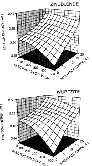
Fig. 2 presents the dependence of the exciton en-ergy on the electric eld intensity and on the quantum well interface width. The exciton energy is shown to decrease when the electric eld is stronger. The rate of decreasing is considerably modied as a consequence of the nonabrupt interface related blue shift of the car-riers energy. As a matter of fact, the exciton energy variation produced by a 500kV/cm electric eld in the zincblende (wurtzite) QW is 53meV (66meV) if their interfaces are sharp, while it is only 27meV (25meV) if the QW interfaces are 10A wide. One can also observe in Fig. 2 that the interface related blue shift of the conned exciton energy in the QWs is stronger when the electric eld intensity increases.
Figure 2. The connement exciton energyEex(w ;l) in 50A
wide zincblende (top) and wurtzite (bottom) nonabrupt GaN/Al0:3Ga0:7N QWs.
IV Concluding Remarks
Although results on the heterointerface characteriza-tion of III-V nitride semiconductor quantum wells are sparse, it is possible to estimate that their in-terface width should be at least of the order of the
GaAs/AlxGa1,xAs QWs (which is about two GaAs
unit cells, i.e. 11A). Recently, a blue shift in
the photoluminescense spectra was associated to QW thickness uctuations, [24] while phonon mode broad-ening in GaN/AlN superlattices was related to the existence of graded interfaces [25], indicating that nonabrupt interfaces should be responsible for im-portant changes on the optical properties of actual GaN/AlxGa1,xN QW structures. The results
pre-sented in this work have highlighted that interface ef-fects in single GaN/AlxGa1,xN QWs can be more
rel-evant than in similar GaAs/AlxGa1,xAs QWs. They
suggest that to a better description of the connement exciton related optical properties, it is necessary to re-sort a nonabrupt description of the GaN/AlxGa1,xN
QWs. The results presented in this work are worth of experimental conrmation.
Acknowledgments
H. Wang would like to acknowledge the visiting sci-entist fellowship he received fromthe Brazilian National Research Council (CNPq) for the development of the research. This work received partial nancial support from CNPq, the Funding Agency of the Ceara State in Brazil (FUNCAP), the Brazilian Ministry of Planning through FINEP.
References
[1] S. Nakamura, T. Mukai, and M. Senoh, Appl. Phys. Lett.64, 1687 (1994).
[2] S. Nakamura, M. Senoh, N. Iwasa, and S. Nagahama, Jpn. J. Appl. Phys.34, L797.
[3] S. Nakamura, M. Senoh, N. Iwasa, S. Nagahama, T. Yamada, T. Matsushita, H. Kiyoku, and Y. Sugimoti, Appl. Phys. Lett.68, 2105 (1996).
[4] S. N. Mohammad and H. Morkoc, Prog. Quantum Elec-tron.20, 361 (1996).
[5] Second International Conference on Nitride Semicon-ductors, ICNS'97, October 27-31. Tokushima, Japan, 1997.
[6] A. Satake, Y. Masumoto, T. Miyajima, T. Asatsunma, F. Nakamura, and M. Ikeda, Phys. Rev B 57, R2401 (1998).
[7] S. Chichibu, T. Azuhata, T. Sota, and S. Nakamura, Appl. Phys. Lett.70, 2822 (1997).
[8] Y. Narukawa, Y. Kawakami, M. Funato, S. Fujita, S. Fujita, and S. Nakamura, Phys. Lett.70, 981 (1997).
[9] G. Mohs, T. Aoki, R. Shimano, M. Kuwata-Gonokami, and S. Nakamura, Solid State Communic. 108, 105
(1998).
[10] T. Y. Chung and K. J. Chang, Semic. Sci. Technol.13,
[11] P. Bigenwald, P. Christol, A. Alemu, B. Gil, J. Crys. Growth189, 119 (1998).
[12] H. Wang, G. A. Farias, and V. N. Freire, submitted to Phys. Rev B.
[13] I. Akasaki and H. amano, Jpn. J. Appl. Phys.36, 5393
(1997), and references therein.
[14] R. J. Radtke, U. Waghmare, H. Ehrenreich, and C. H. Grein, Appl. Phys. Lett.73, 2087 (1998).
[15] V. N. Freire, M. M. Auto, and G. A. Farias, Superlat-ticesand Microstructures11, 17-22 (1992); R. Renan,
V. N. Freire, M. M. Auto, and G. A. Farias,Phys.Rev.
B48, 8446 (1993); E. C. Ferreira, J. A. P. Da Costa,
G. A. Farias, and V. N. Freire, Superlatticesand Mi-crostructures17, 397 (1995).
[16] Y. Ando and T. Itoh, J. Appl. Phys.61, 1497 (1987).
[17] G. Ramrez-Flores, H. Navarro-Contreras, A. Lastras-Martnez, R. C. Powell, and J. E. Greene, Phys. Rev. B50, 8433 (1994).
[18] K. Kim W. R. L. Lambrecht, B. Segall, and M. van Schilfgaarde, Phys. Rev. B56, 7363 (1997).
[19] A. Rubio, J. L. Corkill, M. L. Cohen, E. L. Shirley, and S. G. Louie, Phys. Rev. B48, 11810 (1993).
[20] M. Smith, G. D. Chen, J. Z. Li, J. Y. Lin, H. X. Jiang, A. Salvador, W. Kim, O. Aktas, A. Botchkarev, and H. Morkoc, Appl. Phys. Lett.67, 3387 (1995); S. Strite,
J. Raun, Z. Li, A. Salvador, H. Chen, D. J. Smith, W. J. Choyke, and H. Morkoc, J. Vac. Sic. Technol. B9,
1924 (1991).
[21] B. Monemar, Phys. Rev. B10, 676 (1974).
[22] P. B. Perry and R. F. Rutz, Appl. Phys. Lett.33, 319
(1978).
[23] D. Volm, K. Oettinger, T. Streibl, D. Kovalev, M. Ben-Chorin, J. Diener, B. K. Meyer, J. Majewski, L. Eckey, A. Homann, H. Amano, I. Akasaki, K. Hiramatsu, and T. Detchprohm, Phys. Rev. B53, 16453 (1996);
G. D. Chen, M. Smith, J. Y. Lin, H. X. Jiang, S.-H. Wei, M. Asif Khan, and C. J. Sun, Appl. Phys. Lett.
68, 2784 (1996); A. K. Viswanath, J. I. Lee, D. Kim,
C. R. Lee, and J. Y. Leem, Phys. Rev. B58, 16333
(1998).
[24] M. Smith, J. Y. Lin, H. X. Jiang, A. Salvador, A. Botchkarev, W. Kim, and H. Morkoc, Appl. Phys. Lett.
69, 2453 (1996).