Dye-sensitized Solar Cells: Improving
Lifetime Stability and Performance
Dissertation presented to the Faculty of Engineering of the University of Porto for obtaining the degree of
Doctor in Chemical and Biological Engineering by
José Miguel Lopes Maçaira Nogueira
Adélio Miguel Magalhães Mendes, Full Professor – Supervisor Luísa Manuela Madureira Andrade Silva, Assistant Researcher – Co-supervisor
Department of Chemical Engineering, Faculty of Engineering, University of Porto, Portugal
This work was partially financially supported by: Project POCI-01-0145-FEDER-006939 (Laboratory for Process Engineering, Environment, Biotechnology and Energy – LEPABE) funded by FEDER funds through COMPETE2020 - Programa Operacional Competitividade e Internacionalização (POCI) – and by national funds through FCT – Fundação para a Ciência e a Tecnologia through the Ph.D. grant SFRH/BD/80449/2011, under the Programme POCH/FSE.
© José Miguel Lopes Maçaira Nogueira, 2011-2016
Laboratory for Process Engineering, Environment, Biotechnology and Energy University of Porto – Faculty of Engineering
Rua Dr. Roberto Frias s/n, 4200-465 Porto Portugal
A minha primeira palavra de agradecimento vai para a pessoa que me convenceu a embarcar nesta aventura, o meu orientador, Professor Adélio Mendes. Agradeço o seu apoio, motivação, ensinamentos e amizade. Deixo-lhe uma palavra de apreço e de reconhecimento pela sua enorme capacidade de trabalho, competência e perseverança. Obrigado pela sua disponibilidade e por me ter providenciado condições de trabalho excepcionais. Agradeço também à minha co-orientadora, Doutora Luísa Andrade, pelo apoio e disponibilidade que sempre demonstrou. Obrigado pelas discussões úteis e interessadas, pelos conhecimentos transmitidos, pela sua enorme capacidade de gestão e pela confiança que sempre demonstrou em mim. Deixo ainda uma palavra de reconhecimento aos meus orientadores pela forma como sempre liberaram a minha criatividade. O sucesso deste trabalho também dependeu em grande parte de ambos. Agradeço e reconheço ainda ao Prof. Joaquim Mendes a sua participação essencial nos projectos SolarSel e WinDSC, em particular a selecção da fonte laser utilizada no processo de selagem.
Agradeço à Efacec (Energias Renováveis), parceira dos projectos SolarSel e WinDSC, por ter assumido o risco de investir em I&D. Durante dois anos foi local de trabalho e uma escola. Em particular deixo uma palavra de apreço ao Eng. Nuno Delgado, Eng. Luis de Pessoa Santos, e Eng. Fernando Vaz. Uma palavra especial ao Eng. Nelson Marques, ao Sr. Zé e ao Sr. Jorge pela disponibilidade que sempre demonstraram em ajudar, particularmente na instalação eléctrica da LaserBox.
Um agradecimento especial ao Eng. Fernando Ribeiro, colega de trabalho na Efacec. Parceiro de equipa que rapidamente se tornou num fiel amigo. Obrigado pela tua tempestuosidade e teimosia, causa de profundas discussões técnicas, científicas, filosóficas, políticas e religiosas. Uma combinação improvável que resultou num trabalho puro de equipa e que permitiu a optimização do processo de selagem. Reconheço aqui a tua enorme capacidade técnica e grandíssima dedicação ao projecto SolarSel.
“Solar” (LEPABE, FEUP) liderado pelo Prof. Adélio Mendes, cujo trabalho se desenvolve na UPTEC ‒ Centro de Inovação. Este é um grupo ímpar, multidisciplinar e em constante crescimento onde o ambiente descontraído e condições de trabalho são propícias à excelência dos projectos de I&D.
Aos meus amigos da FEUP pelo companheirismo de sempre, pelos bons momentos passados e pela amizade! Ao João Carneiro, Diana Olariu, Ali Emami, João Silva, Paula Dias, João Mendes, Sara Paula, André Santos, André Maia, Marta Pimenta, Ana Duarte, António Leal, Ricardo Teixeira e Isabel Gomes. Aos meus amigos alfacinhas, João Robalo e Joana Do Vale pelos momentos inesquecíveis que passamos nestes anos, pela cumplicidade e amizade! Aos meus amigos de Espinho, Godinho, Hugo, Jonathan, Mário e Miguel. Amigos de sempre e para sempre! Nestes últimos anos a dedicação aos respectivos trabalhos retirou-nos tempo de convívio, mas não o brilho especial de quando nos juntamos.
Um agradecimento especial à minha família. Fazer parte dela é um privilégio e uma responsabilidade. Obrigado pelos momentos especiais, pelos pilares e valores inabaláveis que têm passado de geração em geração. Uma palavra especial ao Jaime e Marisa, pelas tertúlias com vista de mar que duram até de manhã! Obrigado Tio pelas conversas profundas e intensas! Pelas vivências partilhadas! Um obrigado também à Leonor por nos fazeres trabalhar num futuro melhor. Aos meus sogros, Helena Doutel e Luis Costa pelo apoio constante, pela amizade e pelos bons momentos passados. Aos meus pais, Fernando Nogueira e Maria de Lurdes Maçaira, por serem uma referência de vida, pelo vosso apoio incondicional. Tudo o que sou hoje se deve a vocês. Ao meu irmão, Pedro Maçaira Nogueira, por cresceres comigo, pela cumplicidade, pela personalidade e pelo apoio. Parceiro para a vida!
Por fim, à minha mulher Erica Doutel Costa, o amor da minha vida. Obrigado por seres como és, única! Obrigado por partilhares a tua vida comigo.
A todos que, de uma forma ou de outra, contribuíram para o atingir de mais um objectivo. O meu sincero e humilde obrigado!
Preface
In September 2011 Prof. Adélio Mendes (FEUP) challenged me for developing a glass-to-glass laser sealing by applying his idea of what we later named of scan pattern. This technology was applied to dye-sensitized solar cells, and then what became by being an optimization work evolved into my PhD thesis. This dissertation is submitted for the degree of Doctor of Philosophy at University of Porto – Faculty of Engineering (FEUP). The present work was developed in Laboratory for Process Engineering, Environment, Biotechnology and Energy (LEPABE), at the Chemical Department of FEUP, and at the facilities of EFACEC in Maia. The work was supervised by Professor Adélio Mendes and co-supervised Dr. Luísa Andrade from LEPABE‒FEUP.
From this PhD work resulted the publication of 5 scientific articles and 1 international patent. 1 more scientific article is under revision.
Contents
Dye-sensitized Solar Cells: Improving Lifetime
Stability and Performance
Abstract
xiiiResumo
xivAbbreviations and Symbols
xviChapter 1. Introduction
11.1 Dye Sensitized Solar Cells: Operating principles & State of the art 7
1.2 Nanostructured photoelectrodes 11
1.2.1 Electron transport in nanostructure photoelectrodes 12
1.2.2 1-D nanostructures 14
1.2.3 3-D hierarchically ordered nanostructures 20
1.2.4 3-D template based backbones 24
1.2.5 Hybrid TiO2/Graphene nanostructures 34
1.2.6 Outlook for high performance photoelectrode 38
1.3 Long term stability of DSCs 40
1.4 Scope of the thesis 42
Acknowledgements 43
Chapter 2. Development and Optimization of a laser sealing
process for DSC devices
552.1 Introduction 57
2.2 Materials and methods 58
2.2.1 Glass frit sealant 58
2.2.2 Glass paste thermal conditioning 60
2.2.3 LaserBox equipment 62
2.2.4 Sealing Procedure 64
2.2.5 Thermal cycling tests 64
2.2.6 Leak and shear stress tests 65
2.2.7 DSC performance characterization 67
2.3 Results and Discussion 68
2.3.1 Response surface methodology 68
2.3.2 Process Modeling 69
2.3.3 Influence of the operation conditions 71
2.3.4 Temperature history during the laser sealing process 72
2.3.5 SEM and elemental analysis 74
2.3.6 Leak and shear stress tests 77
2.4 Integration of the laser assisted process in the fabrication of DSCs 78
2.4.1 Sealing process influence on performance of DSC devices 81
2.5 Conclusions 85
Acknowledgments 86
Chapter 3. Laser Sealed Dye-Sensitized Solar Cells: Efficiency
and long term stability analysis
89Abstract 91
3.1 Introduction 92
3.2 Material and Methods 93
3.2.1 Laser sealed DSC fabrication 93
3.2.2 I-V and EIS characterization 95
3.2.3 Accelerated ageing tests 95
3.3 Results and Discussion 97
3.3.1 Photovoltaic performance 97
3.3.2 Electrochemical impedance spectroscopy 100
3.4 Conclusions 104
Acknowledgements 105
References 105
Chapter 4.Temperature Role in the Recombination Reaction
on Dye-Sensitized Solar Cells
107Abstract 109
4.1 Introduction 110
4.2 Material and Methods 112
4.2.1 Laser sealed DSCs and half-cell fabrication 112
4.2.2 Experimental Setup 115
4.3 Results and Discussion 119
4.3.1 Temperature influence in DSC performance 119
4.3.2 Recombination and DSC performance as a function of the temperature 130
4.4 Conclusions 138
Acknowledgements 138
Chapter 5. Modeling, Simulation and Design of
Dye-Sensitized Solar Cells
143Abstract 145
5.1 Introduction 146
5.2 Modeling 149
5.3 Experimental 157
5.3.1 Dye sensitized solar cell preparation 157
5.4 Results and Discussion 158
5.4.1 Current-potential characteristics 158
5.4.2 Influence of recombination in DSCs 160
5.4.3 Interpretation of recombination in charge extraction experiments 167
5.4.4 Optimization of electrode thickness 171
5.5 Conclusions 177
Acknowledgements 178
References 178
Chapter 6. High efficient DSC photoelectrode using a SiO
2scaffold layer coated with a 3 nm TiO
2film
183Abstract 185
6.1 Introduction 186
6.2 Materials and Methods 188
6.2.1 SiO2 scaffold film 188
6.2.2 TiO2 reaction mechanism in ALD 190
6.2.3 Dye sensitized solar cells fabrication 192
6.2.4 DSC performance characterization 193
6.3 Shrinking core model 193
6.4 Results and Discussion 199
6.4.2 Three-dimensional SiO2/TiO2 ALD layer 201
6.4.3 Optical characterization of SiO2/TiO2 films 205
6.4.4 DSCs based on SiO2/TiO2 architecture 207
6.5 Conclusions 217
Acknowledgements 219
References 219
Chapter 7. Concluding Remarks and Outlook
2237.1 Main Conclusions 225
7.2 Outlook for dye-sensitized solar cells 229
References 232
Appendix
233A. Design of Experiments: Design matrix with coded and actual values 235
B. Developed LabVIEW control panel interfaces 236
C. Atomic layer deposition (ALD) process operation details 239
D. Estimation of minimum TIP pulse time for complete coverage of SiO2 scaffold layer with TiO2 film 245
Abstract
Global energy demand is increasing rapidly and by 2030 it is projected that energy consumption will grow 50 %. The Earth serious environmental problems dictate that there is urgency in use clean, secure and affordable energy sources. Photovoltaic (PV) energy is believed to meet these requirements, but up to now PV technology struggles to economically compete with other energy sources. This work studies dye-sensitized solar cells (DSCs), a technology that promises low cost PV energy generation. In particular it addresses the two main bottlenecks that prevent DSC technology to become a commercial alternative; these bottlenecks are lifetime stability and performance.
Concerning stability, encapsulation was identified as critical to obtain stable DSC devices. A new sealing process was developed based on laser assisted glass frit melting. The feasibility of the laser sealing process is investigated and the operating conditions were optimized for sealing DSCs. The sealed samples were subjected to stringent encapsulation tests according to international standards. Accelerated ageing was used to assess the lifetime stability of the laser sealed DSCs and compared with the devices sealed using common polymer materials. The developed laser assisted sealing allowed studying the temperature effect on DSCs performance, in a wide temperature range between - 5 to 105 ºC. The activation energies for the recombination reaction were determined and its dependence on the semiconductor/electrolyte interfaces discussed.
Phenomenological modelling was used as a simulation tool to assess the two main electrochemical processes that rule the DSC performance: electron transport and recombination. The model was used to describe how transport and recombination influence the solar cell efficiency and the optimum design of the photoelectrode (PE).
Finally, a new PE architecture was developed for increasing DSC efficiency. The new architecture aimed at increasing the specific photoelectrode surface area, the transparency and decreasing electron recombination. The developed PE is made of a mesoporous SiO2 scaffold layer coated with a TiO2 film deposited by atomic layer
deposition (ALD). The parameters used at the ALD were optimized and the TiO2 film
thickness that originates the most efficient device determined. The new PE architecture was compared with commercial TiO2 films, and future enhancements in DSC design
Resumo
A procura global de energia está a aumentar rapidamente prevendo-se que até 2030 o seu consumo cresça 50 %. Os graves problemas ambientais do planeta reforçam a urgência em encontrar fontes de energia limpas, seguras e economicamente viáveis. Existe a espectativa de que a energia fotovoltaica (PV) possa cumprir estes requisitos, mas até agora esta tem tido dificuldade em competir economicamente com outras fontes de energia. Este trabalho foca-se no estudo de células solares sensibilizadas por corante (DSCs), uma tecnologia que promete produção de energia elétrica a baixo custo. São abordadas em particular as duas principais limitações que impedem que a tecnologia DSC se torne uma alternativa comercialmente viável: estabilidade a longo prazo e eficiência.
No que diz respeito à estabilidade, o encapsulamento das células foi identificado como fundamental para a obtenção de dispositivos DSC estáveis a longo prazo. Foi desenvolvido um novo processo de selagem baseado na fusão de vidro auxiliada por laser. A viabilidade técnica do processo de selagem laser é investigada e as condições de operação otimizadas. As amostras seladas foram submetidas a testes rigorosos de encapsulação de acordo com normas internacionais. De forma a avaliar a estabilidade a longo prazo da solução desenvolvida, foram realizados testes de envelhecimento acelerado em células seladas a laser e em células seladas com o polímero normalmente empregue.
O processo de selagem laser desenvolvido permitiu também estudar o efeito da temperatura no desempenho das DSCs numa gama alargada de temperaturas entre -5 e 105 °C. As energias de ativação para a reação de recombinação foram determinadas e foi analisada a sua dependência das interfaces semicondutor/eletrólito presentes na célula solar.
De forma a avaliar os dois processos eletroquímicos que regem o desempenho das células DSC, transporte e recombinação de eletrões, foi utilizado um modelo fenomenológico como ferramenta de simulação. O modelo foi usado para descrever de que forma os fenómenos de transporte e recombinação eletrónicos influenciam a eficiência da célula solar e o design ótimo do seu fotoelétrodo (PE).
Por fim, foi desenvolvida uma nova arquitetura para o fotoelétrodo de forma a aumentar a eficiência das DSCs. O novo PE visava aumentar a área de superfície
disponível, a transparência e diminuir a recombinação dos eletrões. O PE desenvolvido é constituído por uma camada mesoporosa de SiO2 cuja superfície interna é coberta por
um filme fino de TiO2 depositado por camada atómica (ALD). Os parâmetros do
processo ALD foram otimizados e a influência da espessura do filme de TiO2 no
desempenho DSCs foi estudada e discutida. O novo PE é comparado com filmes de TiO2 comerciais e foram discutidas implicações futuras no design das células DSC.
Abbreviations and Symbols
Abbreviation
Definition
Units
A active area of the solar cell m2
ALD atomic layer deposition
AM air mass
As specific superficial area m2·g-1
BET Brunauer-Emmett-Teller
BHJ Barrett-Joyner-Halenda
BIPV building integrated photovoltaics
cµ chemical capacitance F
CCE double layer capacitance at the platinum/TCO interface. F
CE counter electrode
Ci concentration of species i M
CTCO/EL
double layer capacitance at exposed TCO/electrolyte
interface F
Da dimensionless number (equivalent to Damkölher number)
Deff effective diffusion coefficient of electrons m2·s-1
Di diffusion coefficient of species m2·s-1
Dk Knudsen diffusivity m2·s-1
dp pore size m
Dref reference diffusion coefficient m2·s-1
DSC dye-sensitized solar cell
dSiO2 SiO2 nanoparticle diameter m
E energy J
E0 redox standard redox energy J
Ea activation energy eV
Ecb conduction band energy J
Ecbc corrected conduction band energy J
Ef Fermi energy J
Efeq dark equilibrium Fermi energy J
Eg bandgap energy J
EIS electrochemical impedance spectroscopy
EOCredox open circuit redox energy J
Eredox redox energy J
F Faraday constant (F = 96 485,3399 C·mol‐1) C· mol‐1
FF fill factor
FTO fluorine-doped Tin oxide
Gi generation rate of specie i m
-3 ·s-1 H Planck constant (h = 6.62606896×10⁻³⁴ J·s) J·s HOMO highest occupied molecular orbital
I electric current A
Is incident photon flux m
2 ·s-1 J0 exchange current density at the counter electrode A·m-2
Ji current density of species i A·m-2
Jrec recombination current A·m
-2
Jsc short circuit current density A·m-2
kB Boltzmann constant J·K-1
kr recombination reaction rate constant m-3(1-β)·s-1 l position coordinate in the SiO2 mesoporous layer m
LAGF laser assisted glass frit
Lf thickness of the DSC mesoporous layer m
Ln electrons diffusion length m
LUMO highest unoccupied molecular orbital
MFC-C N2 flowrate in ALD vacuum chamber cm3·s-1
MFC-R N2 flowrate in ALD reactor cm3·s-1
NCB effective density of states in the TiO2 conduction band m-3
neq dark equilibrium electron density m
-3
ni density of specie i m-3
Ni number of moles of specie i mol
NP nanoparticles
nref reference particle density m-3
P pressure atm
PCE power conversion efficiency %
PE photoelectrode
PV photovoltaic
q elementary charge (q = 1.60217646 × 10‐19 C) C Qfrit quality of the glass frit sealing
Qi flux of specie i m-3·s-1
R ideal gas constant (R = 8.314472 J· K−1· mol−1) J· K−1· mol−1
Rc contact and wire series resistances Ω
Rce charge‐transfer resistance at the counter electrode Ω
Rext load parameter: external resistance Ω
Ri recombination rate of species i m-3·s-1
Rk electron recombination resistance Ω
Rp shunt resistances Ω
Rseries external series resistances Ω
RTCO transparent conductive oxide sheet resistance Ω RTCO/EL
charge transfer resistance at exposed TCO/electrolyte
interface Ω
Rw electron transport resistance Ω
SEM scanning electron microscopy
STP standard conditions of temperature and pressure (273.15 K, 105 Pa)
T temperature K
t time s
TCO thin conductive oxide
Tg transition temperature K
tpurge,i ALD purge time of component i
Ts softening temperature K
UV ultra-violet
Vcb conduction band potential V
Vcbc corrected conduction band potential V
Vext external cell potential V
Vf fermi level potential V
Vint internal cell potential V
Voc open-circuit potential V
wt. weight
X position coordinate in the TiO2 mesoporous layer m X coded factors for the design matrix of the DOE
Xf coverage factor of SiO2 porous layer with TiO2 film %
Z’ real part of impedance Ω
Z’’ imaginary part of impedance Ω
Zd
Warburg element of the Nernst diffusion of I3-within
electrolyte Ω
Greek symbol
Definition
Units
γ coordinate of shrinking core position m
α wavelength-dependent absorption coefficient m-1
β recombination reaction order
Δti ALD pulse time of component i s
ΔVcb shift in the conduction band potential, V V
ΔVint variation of the applied potential, V V
ε porosity
ζ symmetry coefficient
η solar to energy conversion efficiency %
ηinj electron injection efficiency %
ηPt electrochemical overpotential at Pt electrode V
λ wavelength m
ξ tortuosity
ρi molar density of specie i mol·m-3
𝜏e− electron lifetime s
𝜏minp minimum time required for the full coverage SiOlayer with TiO 2 porous
2 film
s
𝜏tr electron transport time s
φ dimensionless number
ϕ dimensionless number (Equivalent to Thiele modulus)
ψ thermal expansion coefficient ºC-1
Superscript
Definition
* dimensionless variable 0- external point of the current collector 0+ xx coordinate close to the photoanode init initial conditions
p pulse t total
Subscripts
Definition
c+ cations CB conduction band CE counter electrode e- electrons ht high temperature I− iodide I3− triiodide lt low temperatureMPP maximum power point
OC open-circuit
SC short-circuit
C
HAPTER
1
Introduction
“The stone age didn’t end because they ran out of stones.” Unknown author
Adapted from the peer-reviewed article
J. Maçaira, L. Andrade, and A. Mendes, Review on nanostructured photoelectrodes for next generation dye-sensitized solar cells. Renewable and Sustainable Energy Reviews, 2013. 27(0): p. 334-349.
1
Introduction
World energy consumption will increase 56 % before 2040 driven by the economic growth and increasing population in developing countries and in emerging economies such as China and India1 – Figure 1.1. Relatively high oil prices, as well as concerns about the environmental impact of the fossil fuels combustion and strong government incentives, have made the harvest of energy from renewable sources the fastest growing energy source according to the International Energy Outlook of 20131.
Figure 1.1 a) World total energy consumption in OECD and non-OECD countries
and b) by fuel type, from 1990 with projections to 2040 (ordinate scale in quadrillion Btu, equivalent to TJ) (adapted from International Energy Outlook 20131)
The total energy generation from renewable sources has increased 2.5 % per year and it is expected to grow from 19 %, recorded in 2008, to 28 % in 20401 – Figure 1.2b). In particular, solar energy is the fastest growing segment of technologies for harvest energy from renewable sources and photovoltaic (PV) market is expected to grow up to 450 GW of installed capacity until 2019, according to the global market outlook for solar power2 – Figure 1.2.
Figure 1.2 Solar PV cumulative market scenarios until 2019 (adapted from Global
market outlook for solar power 2015-2019 2)
Solar energy is the most abundant renewable energy source, and undoubtedly can be regarded as safe, inexhaustible and reliable at a human scale. The total solar power available to the planet Earth exceeds by a factor of 1500 the total human power consumption3. There is huge economic potential in solar energy; however, it is highly dependent on the cost of PV devices. Obviously the PV market evolution will make use of the most competitive solar panels at the time, most likely the first generation crystalline and polycrystalline silicon solar panels (c-Si). These devices at lab scale can achieve up to 25 % sun to power conversion efficiency (PCE, η) and their recent progressively lower prices reflects its industrial establishment that, undoubtedly, makes use of the today’s semiconductor industry infrastructures. However, the high production and environmental costs led to a constant progress in the development and establishment of new PV technologies (Figure 1.3) aiming to avoid the drawbacks of
the c-Si solar panels. Some established semiconductor based technologies comprise gallium arsenide tin film solar cells (GaAs, η ≈ 24 %), copper-indium-gallium-(di)selenide (CIGS, η ≈ 20 %), cadmium-telluride (CdTe, η ≈ 17 %) and amorphous/nanocrystalline silicon (η ≈ 10 %) solar cells4. This second generation of thin film technologies have had an important role in the PV installation capacity up to now5. However, they share the same performance and cost limitations as conventional Si devices. After approximately 20 years of research and development, third generation thin film solar devices are starting to emerge in the marketplace. This new generation of photovoltaic systems includes semiconductor quantum dots (QDPV, η ≈ 6 – 10 %)6, organic semiconductors (OPV, η ≈ 10 %) 4, 7 and dye sensitized solar cells (DSCs, η ≈ 14 %)8. These new technologies benefit from their low processing costs and environmental impact and thus short payback time when compared to the conventional solar devices. At present stage, third generation PV technologies are still far behind the efficiency values of the conventional Si-based solar cells (~ 20 %); nevertheless, the promise of low processing costs and usage of available environmental-friendly raw materials make them subject to an intensive research and development.
Figure 1.3 Best research solar cell efficiencies (courtesy of the National Renewable
Dye sensitized solar cells (DSCs) present themselves as a very promising photovoltaic technology. They are made of cheap components that are non-toxic and world-wide available and offer distinctive features such as semi-transparency, multi-colour range possibilities, flexibility and lightweight applications, but also good performance under low light conditions and different solar incident angles10-12 – Figure 1.4. These unique characteristics open a new possibility of applications and markets where conventional solar devices will never be able to penetrate, e.g. low-power consumer electronics, outdoor or indoor recreational and building integrated photovoltaics (BIPV) applications. In fact, the DSC technology has recently been used by several companies in showcase applications by Glass2Energy, DyePower, Solaronix, Sony, Fujikura, Panasonic, G24i, Dyesol, 3G Solar and Toyota-Asin.
Figure 1.4. Glass façade composed by 300 m2 of dye-sensitized solar cells
demonstration modules in EPFL’s SwissTech Convention Center, Lausanne, Switzerland (adapted from13) .
However, for the DSC technology to become a competitive alternative to the present PV technologies, major breakthroughs are necessary mainly concerning the two critical aspects of any PV device: power conversion efficiency and lifetime.
Regarding the device lifetime, at least 25 years of constant power conversion efficiency should be guaranteed for outdoor applications. This aspect has caught researchers’ attention in order to enhance DSCs’ stability and thus many reports are being published concerning improvements on the stability and new sealing methods
14-19
. Then, several methods were proposed to enhance the efficiency of DSCs20-23, being one of the most promising the use of nanostructured materials as photoelectrodes to enhance light harvesting and charge extraction to improve photocurrent, photovoltage and fill factor.
1.1 Dye Sensitized Solar Cells: Operating principles & State of
the art
In 1991 O’Regan and Grätzel proposed the first bulk heterojuntion photoelectrochemical solar cell with 7 % power conversion efficiency, taking advantage of the three-dimensional TiO2 photoelectrode film and using a ruthenium
dye as sensitizer24. DSCs mimic natural photosynthesis and differ from conventional p-n jup-nctiop-n devices because light collectiop-n ap-nd charge trap-nsport are separated ip-n the cell. Light absorption occurs in the chemisorbed sensitizer molecule, while electron transport occurs in the semiconductor TiO2 - Figure 1.5.
The photoelectrode is a mesoporous oxide layer composed of nanometer-sized particles. Attached to the surface of the oxide is a monolayer of dye responsible for light absorption. The optical absorbance that occurs in the dye molecules results in excitation of an electron from the highest occupied molecular orbital (HOMO) to the lowest unoccupied molecular orbital (LUMO)25. The photogenerated electrons are transferred to the conduction band of the semiconductor oxide and percolate through the semiconductor network, being collected at the transparent conducting oxide. The oxidized dye is regenerated by electron donation from the electrolyte solution containing a redox couple, typically of iodide/triiodide. The triiodide ions formed in the semiconductor’s surface during the redox reaction diffuse to the Pt-catalyzed counter-electrode, where they are reduced back to iodide by the electrons from the external circuit. The efficiency (η) of the solar cell is determined by its current-voltage characteristics, specifically the open-circuit photovoltage (Voc), the photogenerated
current density measured under short-circuit conditions (Jsc), light irradiance (Is) and
the fill factor of the cell (FF), which depends on the series resistances and on the shunt resistances in the cell26 :
𝜂 =𝐽sc𝑉oc
𝐼s FF (1.1)
The short-circuit photocurrent (Jsc) is essentially related to the amount of sunlight
harvested in the visible part of the solar spectrum by the sensitizer. Consequently, dye molecules play a critical role in photon capture and for this reason the progress in DSCs have been closely followed by the constant development of new porphyrin and organic sensitizers that have high extinction coefficients and broader optical absorption spectra. These have even supplanted the commonly used Ru(II) polypyridil sensitizers in liquid but also in solid-state electrolyte DSCs14, 20, 27-35.
The open-circuit voltage (Voc) is related to the energy difference between the
quasi-Fermi level of electrons in the semiconductor and the chemical potential of the redox mediator in the electrolyte36. The most common electrolyte in high performance DSCs uses the triiodide/iodide (I3
-/ I-) redox couple27,37,38. Despite the excellent results achieved so far using this redox couple, it presents some drawbacks such as the corrosion of several current collectors and partial absorption of visible light around 430
nm, resulting in a voltage loss39. To mitigate these effects several alternatives have been studied35, 40-43. Good results have been reported using an amorphous organic hole-transport material (HTM), spiro-OMeTAD (2,2’,7,7’-tetrakis(N,N-di-p-methoxyphenyl-amine)9,9’-spirobifluorene)44 and cobalt based (Co (II/III) tri(bypiridyl)) non-corrosive electrolyte. These new hole transport materials yielded impressive results, reaching PCEs higher than 14 % and Voc of 1 V for liquid-state DSCs and 7.2 % and 965 mV for solid-state devices 8,20,45-50. Other materials like processable p-type direct bandgap CsSnI3 semiconductor have been used very recently
for hole conduction, aiming to replace the liquid iodide/triiodide based electrolyte. This hole conductor yielded record efficiencies of 8.5 % for solid state DSCs51. A very interesting and underexplored class of materials of organometallic halide pervoskite have also been used as sensitizers in liquid electrolyte-based photoelectrochemical cells with conversion efficiencies from 3.5 to 6.5 %52, 53. These materials provide excellent support for binding organic and inorganic components to form a molecular composite that not only acts as a sensitized, but also as a hole and electron conductor. Recently CsSnI3 perovskite was shown to be an efficient hole conductor in a solid state
DSC achieving 8.5 % efficiency51. Another specific perovskite, a methylamonium lead iodide chloride (CH3NH3PbI2Cl), was used as the light absorbing material in
conjunction with TiO2 as transparent n-type component and spiro-OMeTAD as p-type
hole conductor. The device achieved 8 % efficiencies54. Interestingly, the authors found out that by replacing the TiO2 by an insulating framework of Al2O3 the power to
conversion efficiency was improved to almost 11 %. Apparently the perovskite material employed is a much better electron conductor than the TiO2, and the Al2O3
only acts as a “scaffold” to support and provide surface area for the perovkite to be coated on. Other record-breaking work proposed an innovative platform that includes a three dimensional nanocomposite and bilayer architecture with an inorganic-organic hybrid heterojuntion55: the use of TiO2 /CH3NH3PbI3 /polymeric HTMs / Au system
boosted efficiencies of solid state perovskites solar cells up to 20 %. Although this devices have very high efficiencies, they have not yet proven stable enough for commercialization56.
The main processes in a DSC system are light absorption, charge injection, electron transport and collection and electrolyte diffusion. Since 1991 most of the improvements in DSCs efficiency have been achieved through major improvements in molecular sensitizers and redox electrolytes57. However, directly or indirectly all of above mentioned phenomena strongly depend on the photoelectrode. In particular, the two competing processes that rule the performance of a DSC are electron transport in the mesoporous semiconductor and recombination losses in the semiconductor/electrolyte interface58. Both effects have been widely studied mainly using electrochemical impedance spectroscopy (EIS) but there are challenges that still remain particularly in the photoanode36,59-66. Consequently new photoanode structure models are needed to suppress electron recombination and to enhance light harvesting but keeping the cell’s transparency characteristics.
The ideal photoelectrode should have a high surface area to ensure high dye loading and efficient light harvesting. Even though a greater amount of electrons are photogenerated, there is also a higher probability of electrons to recombine in the interface semiconductor/electrolyte – dark current – since the pathway to get the current collector is also higher. Thus, the electron transport in the photoelectrodes plays a very important role in the electron collection efficiency since it directly influences the dark current67. The electron transport is essentially governed by a diffusion mechanism and it is controlled by hoping phenomena limited by the low conductivity of TiO2 nanoparticles and their multiple grain boundaries68. Good
electrolyte diffusion should also be guaranteed in the photoelectrode; however liquid electrolytes tend to have low viscosities, so its diffusion in the photoelectrode should not be a performance-limiting process in DSCs.
Researchers have proposed several strategies to address the transport limiting process, such as using bare 1-D nano-structures composed by TiO2, SnO, or ZnO to
increase electron mobility in the photoelectrode69,70. Although these structures provide direct pathways for electrons to reach the collecting substrate, the inefficient dye adsorption of this type of structures do not generate enough electrons to produce high photocurrents. A common-sense development was to mix high surface area nanoparticles with high conductive 1-D structures and create hybrid photoelectrodes71,
in a way they can benefit from the advantages of each structure. Other approach consists in creating hierarchically ordered photoelectrodes with large aggregate particles composed by smaller ones72-74; this strategy aims to achieve high surface areas, guaranteed by small particles, and efficient electrolyte diffusion, provided by macropores created by the larger aggregates. These photoelectrodes benefit from a good light scattering effect, resulting in high performance devices. Another interesting approach was to use highly conductive host backbones to serve as charge extraction support to the high surface area nanoparticles21,75,76. The idea of having a 3-D TCO collecting substrate has great potential because, if carefully optimized, it should be able to create a DSC where every generated electron can be collected. Following this idea of increasing the photoelectrode conductivity, graphene has also been used in DSCs77-81. Benefiting from its high electrical conductivity and having a work function close to the one of TiO2 (4.42 - 4.5 eV vs. 4.5 eV, respectively), graphene should
enhance electron mobility and extraction in DSCs. These various approaches are described and discussed below.
1.2 Nanostructured photoelectrodes
Nano science has opened the door to the development of new nanostructured materials and concepts that were not available before82-85. Nanostructures such as nanoparticles83,86,87, nanowires88-92, nanotubes88,89,93-96, nanorods97-99 and nanobelts100 have been developed in the last decade for use in an array of applications in electronics, sensor devices, optoelectronics, photovoltaic and photocatalysis84. Nanomaterials can have very high specific surface areas even up to several hundred of m2∙g-1101,102. Photoelectrodes of nanomaterials allow the adsorption of a large amount of sensitizer molecules in a monolayer configuration; the dye coated area relates to the photocurrent generated by the DSC device. Nanosize materials also affect the way electrons are transported through the photoelectrode structure. Unlike p-n junction solar cells, in DSCs there is no macroscopic electrostatic potential gradient in the film, fact caused by the small size of the individual colloidal particles and by the presence of concentrated electrolytes. This means that in the nanoparticle film the governing
electron transport process is diffusion, contrary to the drift process seen in p-n junction solar cells for carrier separation in the presence of an electrical field25,103.
The most common material found in DSC’s photoelectrode is anatase TiO2. This
commercial metal oxide has typically surface areas between 40-100 m2 and an electric resistivity in the order of 1to 102 Ω·cm 104, 105.
1.2.1 Electron transport in nanostructured photoelectrodes
The typical electron diffusion coefficient in TiO2 nanoparticle film, 5×10⁻⁵
cm2·s-1, is found to be several orders of magnitude below single crystal (bulk) values106-108. The higher electron mobility and diffusion coefficients in single crystals are related to their higher electron concentrations (caused either by illumination or application of external voltage)67,109. The values determined for the electron diffusion coefficients point out the fact that diffusion is much slower in nanostructured materials than in single crystals; this is related to the multicrystalline nature of these structures that creates electron traps and consequently limit the lifetime of the excited electrons67. Although still subject of some debate67,110,111, it is generally accepted that electron transport occurs by the combination of two phenomena: percolation through a network of sites and thermal accessibility to energy states. Therefore, morphological parameters such as porosity, surface area, pore size, particle diameter, shape and elemental crystal size and orientation within the nanostructures have an important impact on the electron diffusion coefficient but also in the energetic properties of the material, such as the distribution of trap energy or electronic concentration.
The electron transport and recombination properties can be studied by several techniques, including photocurrent/photovoltage transient techniques112,113, intensity modulated photocurrent spectroscopy (IMPS)/intensity modulated photovoltage spectroscopy (IMVS)106,114 and by electrochemical impedance spectroscopy (EIS)59,115. In particular EIS is a powerful technique for investigating the kinetic processes of DSCs. Electron transport and chemical potential in the semiconductor film, electron recombination in the photoelectrode/electrolyte interface, charge transfer at the counter electrode and the diffusion of the redox species in the electrolyte can be well distinguished based on the impedance response of the system as a function of
frequency. Compared to the other techniques, EIS has the potential to allow obtaining most parameters that reflect the kinetic processes of the device. Making use of the Nyquist plots, the impedance data is fitted by an adequate equivalent circuit and the electron transport and recombination properties parameters are estimated. From these experiments three main parameters can be obtained: the recombination resistance, Rk,
transport resistance, Rw and chemical capacitance of the semiconductor Cμ. In this way
the electron diffusion length, 𝐿n, and the electron lifetime, 𝜏e− , can be determined by
using the following equations65:
𝜏𝑒−= 𝑅k𝐶μ (1.2)
𝐿n= 𝐿f√𝑅k 𝑅w
(1.3)
𝐿n= √𝜏n𝐷eff (1.4)
where Deff is the electron diffusion coefficient and 𝐿f is the semiconductor film
thickness. Combining eq.(1.2) and eq.(1.3) the effective diffusion coefficient of electrons in the semiconductor can be determined by:
𝐷eff= (
𝑅k 𝑅w) (
𝐿2f
𝜏n) (1.5)
Using the electron diffusion coefficient the electron transport time, 𝜏tr , can be
determined by116,117:
𝜏tr = 𝐿f
2
𝐷eff (1.6)
This value indicates for how long an electron can percolate through the semiconductor before recombining with electrolyte. Before the electrons can be collected at the FTO substrate there is the possibility of recombination with the electrolyte, so an electron collecting rate at the FTO substrate should be defined20. Based on the two processes that rule the performance of a DSC, recombination and transport, a collection efficiency, ηcc, can be determined by
118
𝜂cc=[−𝐿n𝛼 cosh ( 𝐿f 𝐿n) + sinh (𝐿𝐿nf) + 𝐿n𝛼𝑒−𝛼𝐿f] 𝐿n𝛼 (1 − 𝐿n2𝛼2)(1 − 𝑒−𝛼𝐿f) cosh (𝐿f 𝐿n) (1.7)
where α is the photoelectrode film absorption coefficient.
1.2.2 1-D nanostructures
Considerable attention has been given to the fact that morphological features can have a clear impact in the performance of photoelectrodes in dye-sensitized solar cells, mainly in the electron transport effectiveness and the electron recombination with electrolyte. Particular interest is given to 1-D nanostructures that are believed to improve electron transport by providing direct pathways throughout the structure of the photoelectrode to the collecting substrate. The so-called 1-D structures include nanotubes, nanowires and nanofibers that can be composed by several metal oxide materials such as TiO2 ZnO or SnO2
69,70
. Generally, these materials have higher diffusion coefficients than non-ordered nanostructures and are meant to give electron diffusion lengths larger than film thickness. These structures can be used directly as photoelectrodes with dye molecules adsorbed in their surface – Figure 1.6 a) – or by adding metal oxide nanoparticles to the 1-D structure – Figure 1.6 b). Table 1.1 presents the diffusion coefficients as well as the corresponding cell performance characteristic values for several DSCs produced with photoelectrodes based on 1-D nanostructures. The values presented in Table 1.1 show that 1-D nanostructures present higher values of diffusion coefficients than nanoparticle based structures, meaning that generated electrons can move and reach the collecting substrate faster. However the overall DSC performance is far from the ones obtained using the conventional TiO2
nanoparticle film. This is mainly attributed to the comparatively low internal surface area available for the adsorption of dye molecules.
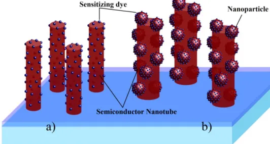
Figure 1.6 a) Schematic of 1-D nanostructures with sensitizing dye adsorbed on the
surface; b) 1-D nanostructures decorated with semiconductor nanoparticles.
Table 1.1 1-D nanostructured DSC performance values and electron diffusion
coefficients.
1-D Nanostructure Ref.
Cell performance Diffusion
coefficient η / % Jsc / mA∙cm-2 Voc / mV FF Deff / cm 2∙s-1 N719 TiO2 NP 119 5.00 11.3 670 0.660 7.2×10⁻⁵
Mercurochrome-sensitized ZnO nanowire 119 0.84 3.40 500 0.490 1.8×10⁻³
Mercurochrome-sensitized ZnO nanowire/ NP composite 119 2.20 6.30 610 0.580 2.1×10⁻⁴ TiO2 NP/nanotubes, 10 wt. % 71 3.10 8.33 630 0.600 7.1×10⁻⁴ TiO2 nanorods 120 0.56 2.22 575 0.440 3.3×10⁻⁷
TiO2 nanorods coated with ZnO nanoparticles
120
0.83 3.57 545 0.430 8.0×10⁻⁶
TiO2 nanorods coated with TiO2 nanoparticles 120 0.19 0.71 592 0.470 4.3×10⁻⁶
Kang et al.121 were one of the first authors to report good performance values with semi-transparent DSCs using a photoelectrode composed only by nanotubes. They produced nanotube arrays with external diameter of 295 nm, tube lengths of 6‒15 μm and wall thickness of 21‒41 nm, respectively – Figure 1.7. The incorporation of this material in a DSC configuration exhibited a Voc of 610 mV, a Jsc of 8.26 mA∙cm
-2
and a fill factor of 0.70, giving an overall power conversion efficiency of 3.5 %. Although
these results are an improvement for nanotube-based DSC photoelectrodes, the TiO2
nanoparticle-based DSCs still presents higher performance. As mentioned earlier, the low surface area of these types of 1-D nanotube arrays can explain the relatively low efficiency of the corresponding DSC devices.
Figure 1.7 Field emission-SEM images TiO2 nanotubes
121 .
To overcome the low surface area that 1-D nanostructures have compared with nanoparticle films, some researchers combined both structures in order to take advantage of the benefits of each of them122,123. Gan et al.123 created a hybrid structure combining vertically aligned ZnO nanowires (NW) with TiO2 nanoparticles (NP)
attached. ZnO has similar band gap of 3.2 eV124 but electron mobility up to two orders of magnitude higher than TiO2: (0.1 ‒ 4) cm
2
·(V·s)-1
vs. 65 cm2·(V·s)-1
at 25 ºC, respectively70,105, 125-127. This makes ZnO a particularly interesting metal oxide to compete with TiO2 in DSCs. The high value of Deff of ZnO NW – based DSC
substantiates that the electrons injected from excited dye molecules can travel faster and therefore are collected more efficiently - Figure 1.7. However, the low value of Jsc
in the bare ZnO electrode confirms the low surface area of these 1-D aligned nanostructures. Incorporating TiO2 NPs with inherent high surface areas in the ZnO
nanowires, an increase in the current density from 1.60 to 3.54 mA∙cm-2 was obtained by these authors. The hybrid cell revealed a Deff value of 6.92 × 10
-4
cm2∙s-1 that falls between those of the bare ZnO film (2.8×10⁻³ cm2∙s-1) and the TiO2 NP electrode (≈ 5 ×
10-5 cm2∙s-1) ‒ Table 1.2. Actually, it is almost fifteen times larger than the Deff of TiO2
improved electron transport along the vertically aligned nanowire array and increased surface area provided by the TiO2 NP. Nevertheless, the performance of the hybrid cell
(2.2 %) is still far from the nanoparticle-based DSC (5 % in Table 1.1), mainly because the surface area provided by the hybrid solution is still low compared to a similar thickness film constituted only by nanoparticles. This fact was caused by the low coverage of the nanowires with nanoparticles as shown in Figure 1.8 and Table 1.2, as well as the low thickness of the hybrid photoanode (3 μm). Nonetheless, better results can be expected if an optimization is performed to balance the ratio between the vertically aligned structures and the quantity of nanoparticles attached to their surface.
Figure 1.8 SEM images of vertically aligned nanowires: (a) without and (b) with NP
attached to its surface 123.
Table 1.2 DSC performance parameters and diffusion coefficients, correspondent to
devices using the photoelectrodes presented in Figure 1.8.
Electrode Jsc mA·cm2 Voc / mV FF η / % τ/ ms Deff / cm2·s-1
TiO2 NP 2.52×10⁻⁵
ZnO NW 1.60 610 0.40 0.390 84.0 2.80×10⁻³
ZnO NW/TiO2 NP 3.54 600 0.37 0.790 57.3 6.92×10⁻⁴
A common strategy to achieve high electron mobility but also high surface area is blending 1-D nanostructures, such as TiO2 nanotubes, with TiO2 nanoparticles; this
way the photoelectrode can benefit from both the high conductive 1-D nanostructure and from the high surface area available for dye adsorption – Figure 1.9.
Figure 1.9 Schematic of 1-D nanostructures blended with metal oxide particles.
Zhong et al.71 showed that it is possible to increase the photovoltaic performance of DSCs by blending different concentrations of TiO2 nanotubes into a TiO2
mesoporous film. These authors blended anodic TiO2 nanotubes with different
concentrations into a P25 based TiO2 mesoporous film and studied the electron
transport properties of the film and the recombination phenomena by electrochemical impedance spectroscopy ‒ Figure 1.10. Although this study uses a low performance TiO2 reference electrode (0 wt. % of nanotubes) it provides complete EIS data allowing
to withdraw important conclusions about the use of nanotubes in DSC photoelectrodes.
Figure 1.10 (a) SEM micrograph of nanotubes sinthetized by Zhong et al.71; (b)
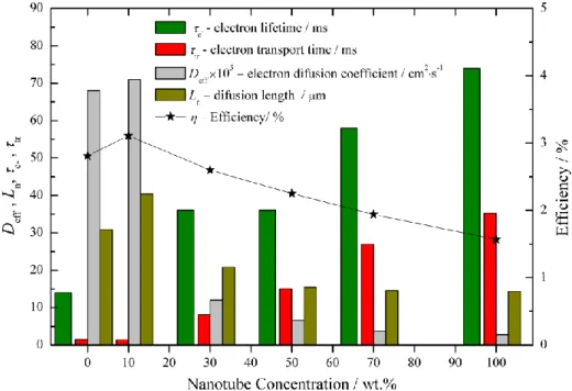
The same authors optimized the concentration of nanotubes blended in the photoelectrode film, increasing electron transport and slowing the electron recombination. Figure 1.11 presents the electron properties of DSCs with different nanotube concentrations. There is a correlation between the device’s efficiency and the electron diffusion coefficient, electron diffusion length and ultimately with the electron collection efficiency. The interpretation of the diffusion length, Ln, reflects the main
phenomena occurring in DSCs: the electron transport and electron recombination. For a nanotubes concentration of 10 wt. %, η and Deff present maximum values. For a
blending level of 10 wt. % nanotubes dispersed in the TiO2 particles supply shorter
paths for electron transport than the disordered interconnected TiO2 nanoparticles. For
a 30 wt. % nanotubes concentration, the decrease in the device efficiency is followed by the decrease of the electron diffusion coefficient and electron diffusion length due to the increase of the electron transport time. So, in this specific case, the concentration of TiO2 nanotubes might be acting as trap centers that difficult transportation to FTO
substrate. Although the TiO2 nanotubes are more conductive than TiO2 nanoparticles,
above a certain concentration the increase of nanotubes does not result in higher electron diffusion coefficients in the film. For concentrations higher than 30 wt. %, the electron lifetime increases even though the global efficiency of the device decreases. In fact, the ratio between electron lifetime and transit time becomes constant, meaning that the recombination resistance decreases at the same level of the transport resistance increases; thus the electron diffusion length remains approximately constant. Therefore, the low photocurrent density explains the efficiency decrease since the inclusion of nanotubes above 30 wt. % strongly diminishes the available surface area for dye adsorption.
Figure 1.11 Electron transport properties and DSC performance value of DSCs with
different nanotube concentrations (adapted from71).
1.2.3 3-D hierarchically ordered nanostructures
The key aspects of a photoelectrode structure are large surface area, necessary to ensure high loading of dye molecules that will generate electrons, and sufficiently large pores with excellent interconnectivity for efficient electrolyte diffusion. Additionally, the defect level and the number of particle boundaries must be low to suppress electron loss by recombination with the electrolyte and allow a good electron transport to the collecting substrate. However, in a standard TiO2 nanostructure high surface area and
large pores are not compatible. Even if an increase of the surface area is important to adsorb a great amount of dye, it simultaneously decreases the average pore size, thus limiting the diffusion of the redox species in the nanostructure. As stated before, 1-D vertically aligned structures solve the electron transport issue and facilitate the electrolyte diffusion throughout the photoelectrode, but do not ensure enough dye loading that could result in high performance devices. This way, 3-D hierarchical pore structures are very interesting as they have several scales of pores. Indeed, such
materials are of great interest as they provide high surface areas and large pore sizes at the same time: nanometer pores that ensure high amount of adsorbed dye molecules - Figure 1.12 (II) ‒ and large micro or mesopores that allow fast electrolyte diffusion - Figure 1.12 (I)72-74.
Figure 1.12 Schematic representation of a hierarchical nanoparticle film, having two
different scale pores: (I) meso/macropores and (II) smaller nanopores.
Kim et al.128 developed a solvothermal method for preparing crystallized TiO2
sphere with ultrahigh surface areas up to 117.9 m2∙g-1 and a well-defined nanoporous structure. The strategy used for the preparation of these spheres involves a two-step approach. First, the controlled hydrolysis reaction (equation 1.8) is carried out to form the TiO2:
Ti{OCH(CH3)2}4+ 2H2O → TiO2+ 4(CH3)2CHOH (1.8)
This reaction produces TiO2 spheres in the amorphous phase and with a smooth
surface without any pores - Figure 1.13a). The shape and size of the spheres can be controlled by the conditions of the hydrolysis reaction128. Then, the formed spheres are collected and washed with ethanol, and transferred to a titanium autoclave containing ethanol to conduct a hydrothermal reaction. The temperature is raised to 240 ºC and held for 6 h; by this means the amorphous spheres are converted to a crystallized structure with high porosity - Figure 1.13b) and c).
Figure 1.13 SEM micrographs of the spheres synthesized by Kim et al.128: a) before and b) after the hydrothermal treatment and c) TEM image with detail showing the porosity of the spheres.
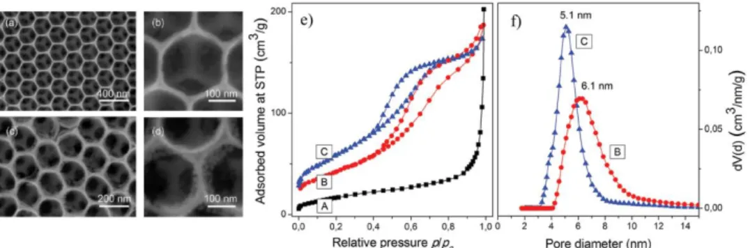
The produced spheres have a diameter of 250 nm. The Brunauer-Emmett-Teller (BET) surface area of these structures was measured to be up to 117.9 m2∙g-1, which is 1.7 times higher than the usual surface area of a P25 film. This is an indication of the high internal surface area built in the spheres. The authors also measured the pore size distribution and found that, as expected, the spheres exhibit a bimodal pore size distribution. The N2 adsorption-desorption isotherms showed that the TiO2 nanoparticle
film has mainly pores of 29 nm, while the spheres show pores with average pore sizes of 9 nm and 55 nm. The smaller pores are inside the nanoporous sphere, visible in Figure 1.13c), and they are responsible for the high surface area of the final structure. The 55 nm sized pores are originated by the interstitial voids formed by the close-packed 250 nm spheres and they are responsible for the electrolyte diffusion improvement throughout the film. The internal pore of ~ 9 nm did not affect the diffusion of the electrolyte probably because the diffusion length is only ≈125 nm (half of the bead diameter = 250 nm). The spheres were used to prepare TiO2 electrodes with
thicknesses in the range of 10 ‒ 10.3 μm. The resulting DSCs revealed a high Jsc of 14.6 mA∙cm-2
, a Voc of 804 mV, a FF of 0.72 and an efficiency of η = 8.44 %. These
values are considerable better than the results obtained for a standard nanoparticle TiO2
film: Jsc of 12.7 mA∙cm -2
, a Voc of 811 mV, a FF of 0.72 and an efficiency of η = 7.40
%. The main difference between both types of DSCs is the short-circuit current density Jsc that was considerably enhanced. This increase is mainly ascribed to the increased
the cell equipped with the new photoelectrode and 122.1 μmol∙cm-2
for the conventional cell. Additionally, the produced photocurrent should also benefit from scattering effect of the larger 250 nm particles in the photoelectrode. The same authors added to the previous photoelectrode a 500 nm interfacial TiO2 layer to decrease the
electron recombination at the FTO/electrolyte interface. The TiO2 spheres were then
treated with TiCl4 and, finally, the photoelectrode outer surface was coated with hollow
TiO2 nanoparticles to act as scattering layer. The final DSC device showed an excellent
result of 19.6 mA∙cm-2
of Jsc, a Voc of 766 mV, a FF of 0.69 and an efficiency of η =
10.52 %.
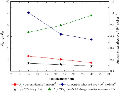
Sauvage et al.23 reported a single titania layer based on the same principle, using mesoporous beads of 830 nm ‒ Figure 1.14. The reported bead film had 89 m2∙g-1 and a mean pore size of 23 nm. The beads showed a mesoporous structure from the surface to the core and therefore the interior titania nanoparticles remain highly accessible to both chemisorption of dye molecules and electrolyte diffusion. The authors also presented evidences that inside the beads exist densely packed TiO2 grains, having
each grain contact with the neighbouring ones. This aspect is responsible for the increase of electron lifetime and enhanced electron mobility, reducing the electron recombination effect with the electrolyte.
Figure 1.14 SEM micrographs of the obtained beads prepared by Sauvage et al.23
showing: (a) their close packing in the film and (b) the high mesoporosity to the core.
The authors reported 10.6 % efficiency and an IPCE of 92 % at a wavelength of 570 nm with a 12 μm single bead film and using a heteroleptic tiophene-based dye (C101 dye). However, using the standard N719 dye with the above mentioned semiconductor structure resulted in a DSC with only 8.3 % efficiency. This allows concluding that the morphology and chemical nature of both nanoparticle film and dye molecule must be optimized for each other. The same authors found that the solar cells prepared with bead film showed enhanced electron lifetime, electron diffusion coefficients and diffusion length compared to a P25 film. The superior performance of the beads was mainly attributed to the close packing of grains and crystal intergrowth within the mesoporous titania beads. Similarly to what Kim et al. 128 have done, a triple layer DSC was prepared by Sauvage et al.23, combining mesoporous beads with a transparent P25 TiO2 interfacial layer and a light scattering layer on top of the beads,
rendering an impressive Jsc of 19.90 mA∙cm -2
, a Voc of 724 mV, a FF of 0.77 and an η
of 11.2 %. Even though the higher efficiency obtained based on a complex structure it is impressive that a single 12 μm film of TiO2 beads gave 10.6 % PCE.
1.2.4 3-D template based backbones
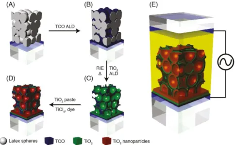
Other types of hierarchical systems include structures with different length scales with different physical properties, e.g. systems including larger backbones with several pore and crystal sizes. It was reported to be possible to create hierarchical structures with individual control over the macro and mesostructure morphologies and dimensions, by infiltration of mesoporous amorphous silica in macroporous ceramic129 or titania backbones130.
Figure 1.15 Schematic representation of the preparation method of hierarchical
titania frameworks. A template material, such as polystyrene spheres, is impregnated with a titania solution precursor that after the hydrolization reaction is calcinated to form the crystallized anatase backbone, adapted from76.
This approach was later used to create fully crystalline hierarchical titania backbones, as reported by Kuo et al.131. This work revealed a novel multi-scale TiO2
nanostructure, composed by a TiO2 blocking layer at the FTO surface and an inverse
opal main structure. Then, organized transport channels were created between contacting spherical voids of the TiO2 inverse opal and then TiO2 nanoparticles were
coated on the spherical surfaces of the voids ‒ Figure 1.16. The TiO2 inverse opal film
was created by coating the blocking layer with polystyrene spheres (PS) with 100 nm of diameter. The PS template was infiltrated by electrochemical deposition of TiO2 ‒
Figure 1.16a) ‒ and a close packing of PS spheres was obtained – Figure 1.16b). Afterwards, the resulting PS template was removed by calcination to obtain a crystalline inverse opal anatase scaffold opal Figure 1.16 c) and d). Then, this structure was treated with TiCl4 in order to introduce TiO2 NP into the structure and then to
Figure 1.16 a) Schematic representation of the synthesis method of a highly ordered
multi-scale nanostructure of TiO2 proposed by Kuo et al.131; b) Film composed by the polystyrene opals revealing their close packing; SEM micrographs of the TiO2 inverse opal c) before and d) after TiCl4 treatment; e) TEM images of the TiO2 nanoparticle decorated inverse opal revealing the coating of the macroporous transport channels. Adapted from131.
Figure 1.16 c) and d) present SEM pictures of the anatase inverse opal structure before and after the TiCl4 treatment. These figures show TiO2 NP of 10‒15 nm
attached to the backbone, as well as the transport channel openings of 30~50 nm for dye solution and electrolyte penetration. Similarly to the bead structures presented before, these features are believed to enhance the load of dye molecules and electrolyte diffusion within the structure. The TEM picture presented in Figure 1.16 e) shows that TiO2 NP are well crystallized and well connected, characteristics that are essential for a
good electron transport through the structure. Because the NP are organized and attached to the walls of the main large pores, they have excellent access to the electrolyte. The fabricated TiO2 nanostructure was assembled in a DSC configuration,
yielding a Jsc of 8.2 mA∙cm -2
, a Voc of 720 mV, a FF of 0.62 and an efficiency of η =