PROGRAMA DE PÓS-GRADUAÇÃO EM CIÊNCIA E ENGENHARIA DE MATERIAIS
IN SITU TRANSMISSION ELECTRON MICROSCOPY STUDY OF NANOSTRUCTURE MIXED OXIDES AT HIGH TEMPERATURES
Santiago Maya Johnson
PROGRAMA DE PÓS-GRADUAÇÃO EM CIÊNCIA E ENGENHARIA DE MATERIAIS
IN SITU TRANSMISSION ELECTRON MICROSCOPY STUDY OF NANOSTRUCTURE MIXED OXIDES AT HIGH TEMPERATURES
Santiago Maya Johnson
Thesis presented to the Post-Graduate Program in Materials Science and Engineering as a partial requirement to obtain the title of DOCTOR OF SCIENCE AND MATERIAL ENGINEERING
Advisor: PhD, Edson Roberto Leite
Funding agencies: CNPq process nº 140517/2015-4, e FAPESP process nº 2015/07044-9.
To my mother, Olga María Johnson, who always believed in me, and taught me that if you do something, you should do it the right way ... otherwise, it is better not to do it. She was my first teacher and aroused the curiosity that exists inside me; always ask, why?...
I just hope to live up to all their sacrifices.
DEDICATÓRIA
A mi madre, Olga María Johnson, quien siempre creyó en mí, y me enseño que si haces algo, se debe hacer de la manera correcta… sino, mejor no hacerlo. Fue mi primera profesora y despertó la curiosidad que hay en mí; siempre preguntar, ¿por qué?...
Sólo espero estar a la altura de todos sus sacrificios.
RESUME
Master of Engineering - Materials and Process - National University of Colombia, Medellin, Colombia (2014)
ACKNOWLEDGEMENTS
Firstly, I would like to express my sincere gratitude to Prof. Antonio José Ramirez, for giving me their confidence and allowing me to work on this challenging project. Also, I would like to express my gratitude to my advisor Prof. Edson R. Leire, who provided me an opportunity to join their team, and who gave access to the laboratory and research facilities. Without they precious support it would not be possible to conduct this research.
I would like to thank my fellow labmates in the LNNano – CNPEM in Campinas, who received me in Brazil, and made me feel at home. The Julian’s, Eduardo, Thais, Leonardo, Victor, Joel, and many others that I forget to name. Thanks for the stimulating discussions, the portuguese lessons, for working together, and above all, for all the fun moments we share together.
I would like to thank my fellow labmates in the LIEC – UFSCar in São Carlos, who taught me so many new things, and with whom I shared such good moments. The Bruno’s, Julio, Everton, William, Andressa, Renata, Mario, Régis, and all the others. Thanks for the stimulating discussions, the talks in the corridors, for your support and help.
My sincere thanks to all my friends, Juan Pablo, Dario, Ramon, Monica, Claudia, Rodolfo, Jeanine, and everyone with whom I shared during these last four years. Thanks for the laughs and the good times, and above all, for sharing your time with me, the most valuable thing that we all have.
Last but by no means least, thanks to Leidy, who has accompanied me (and has tolerated me) during these last years, by his side everything has become easier, the penalties and sacrifices have been divided, and the joys and achievements have been added.
Also, thanks to Brazil for giving me the opportunity to do my Ph.D., hosting me and allowing me to be part of their society.
This study was financed in part by the Coordenação de Aperfeiçoamento de Pessoal de Nível Superior - Brasil (CAPES) - Finance Code 001.
ABSTRACT
This work addresses the characterization of the high temperature reactions between different nanoparticles oxides, CeO2-ZrO2 and CeO2-SnO2, by the direct observation of the phenomenon by in situ Transmission Electron Microscopy (TEM). The nanoparticles were synthesized via three different synthesis methods, hydrothermal, solvothermal, and solvent-control. The changes in the size and morphology of the nanoparticles, the interactions that lead to processes of sintering / densification, and the phase transformations that occur during the experiments were documented. Also, a detailed study of the influence of the electron beam current density on the sample, and its synergism with the temperature during the in situ experiments was performed. The interactions between the oxide metal nanoparticles and the films of the TEM grids showed a great influence during the in situ tests at high temperature. For the experimental setups tested in this work, the main mechanism of interaction between the nanoparticles was oriented attachment.
Keywords: High-Resolution Transmission Electron Microscopy (HRTEM); in situ Transmission Electron Microscopy; metal oxide nanoparticles; nanoparticle
RESUMO
ESTUDO DE MICROSCOPIA ELETRÔNICA DE TRANSMISSÃO IN
SITU DE NANOESTRUTURA DE ÓXIDOS MISTOS EM ALTAS
TEMPERATURAS
Este trabalho aborda a caracterização das reações em alta temperatura entre diferentes nanopartículas de óxidos metálicos, CeO2-ZrO2 e CeO2-SnO2,
pela observação direta do fenômeno pela Microscopia Eletrônica de Transmissão (MET) in situ. As nanopartículas foram sintetizadas através de
três diferentes métodos de síntese, hidrotérmico, solvotérmico e controle de solvente. As mudanças no tamanho e morfologia das nanopartículas, as interações que levam a processos de sinterização/densificação e as transformações de fase que ocorrem durante os experimentos foram documentadas. Além disso, um estudo detalhado da influência da densidade de corrente do feixe de elétrons na amostra e seu sinergismo com a temperatura durante os experimentos in situ foram realizados. As interações
entre as nanopartículas de óxidos metálicos e os filmes das grades (grids) para MET mostraram grande influência durante os testes in situ em altas
temperaturas. Para as configurações experimentais testadas neste trabalho, o principal mecanismo de interação entre as nanopartículas foi a fixação orientada (oriented attachment).
Palavras-chave: Microscopia Eletrônica de Transmissão de Alta Resolução
(HRTEM); Microscopia Eletrônica de Transmissão in situ; nanopartículas de
PUBLICATIONS
- MAYA‐JOHNSON, SANTIAGO; GRACIA, LOURDES; LONGO, ELSON; ANDRES, JUAN; LEITE, EDSON R. Synthesis of Cuboctahedral CeO2 Nanoclusters and Their Assembly into Cuboid Nanoparticles by Oriented Attachment. In: CHEMNANOMAT 3 (4), 228-232; 2017.
- SCZANCOSKI, JÚLIO; MAYA‐JOHNSON, SANTIAGO; DA SILVA PEREIRA, WYLLAMANNEY; LONGO, ELSON; LEITE, EDSON R. Atomic diffusion induced by electron-beam irradiation: An in situ study of Ag structures grown from α-Ag2WO4. In: Crystal Growth & Design (Submitted 16-Jul-2018)
Posters presented in Congresses and Conferences
- S. Maya-Johnson, Edson R. Leite; Synthesis and Characterization of CeO2 Nanoclusters with a Very Narrow Size Distribution. 7th Latin American Conference on Metastable and Nanostructured Materials, NANOMAT 2017; Brotas – SP.
- Santiago Maya Johnson, Edson Roberto Leite, Lourdes Gracia Edo, Juan Andrés, and Elson Longo; A Theoretical and Practical Approach to the Formation of CeO2 Cuboid Nanoparticles from the Synthesis and Assembly of Cuboctahedral Nanoclusters by Oriented Attachment. XVI Brazilian MRS Meeting, 2017; Gramado – RS.
INDEX
Pág.
DISSERTATION COMMITTEE ... i
ACKNOWLEDGEMENTS ... iii
ABSTRACT ... v
RESUMO ... vii
PUBLICATIONS ... ix
INDEX ... xi
LIST OF TABLES ... xiii
LIST OF FIGURES ... xv
SYMBOLS AND ABBREVIATIONS ... xxv
1 INTRODUCTION ... 1
2 LITERATURE REVIEW ... 5
2.1 A brief summary of Cerium, Zirconium, and Tin oxide ... 5
2.2 Phase diagrams and solubility ... 7
2.3 Conceptual Framework ... 10
2.3.1 Electron microscope ... 10
2.3.2 Nanoparticle synthesis ... 22
2.3.3 Solvents ... 26
2.4 Related works in in situ electron microscopy ... 30
3 MATERIALS AND METHODOLOGY ... 41
3.1 Synthesis of the nanocrystals ... 41
3.1.1 Synthesis of Ceria nanocrystals ... 41
3.1.2 Synthesis of Zirconia nanocrystals ... 43
3.2 Characterization techniques ... 44
3.2.1 X-Ray Diffraction ... 44
3.2.2 Thermal analysis ... 44
3.2.3 Infrared spectroscopy ... 44
3.2.4 Transmission electron microscopy ... 45
3.3 Mixture of the nanocrystals ... 46
3.4 Remotion of the organic layer ... 51
3.6 Ex situ experiments ... 57
3.7 In situ TEM experiments at high temperature ... 57
4 RESULTS AND ANALYSIS ... 59
4.1 Synthesis of Ceria nanocrystals... 59
4.2 Synthesis of Zirconia nanocrystals ... 77
4.3 Ex situ tests ... 80
4.4 The dose-rate threshold of beam damage ... 86
4.5 In situ tests ... 90
4.6 The in situ tests in the literature ... 110
5 CONCLUSIONS ... 123
6 SUGGESTIONS FOR FUTURE WORKS ... 125
7 BIBLIOGRAPHY ... 127
APPENDIX A: SYNTHESIS OF TIN OXIDE NANOCRYSTALS ... 137
LIST OF TABLES
Pág.
Table 3.1 - Reagents used for the production of nanocrystals ... 41 Table 3.2 - Specifications overview of the TEMs located in the UFSCar, and LNNano/CNPEM. ... 45
Table 3.3 - Mass loss, radius, and density of the CeO2 and ZrO2 nanoparticles. ... 46
LIST OF FIGURES
Pág.
Figure 1.1 - Number of scientific publications per year related to nano, nanotechnology or in situ microscopy. ... 2
Figure 2.1 - Tentative phase diagram for the ZrO2-CeO2 system, proposed
by Duran et al [45]. 8
Figure 2.2 - a) XRD patterns of CeO2-SnO2 mixed oxides, variation from 0 to 0.20 mol % of tin oxide [43], and b) comparison of the two pure oxides with a mixture with Sn/Ce atomic ratio of 2:1 corresponding to 33mol % of CeO2 [41]. The red arrows in (a) indicate the appearance of tin oxide at 15mol %; in (b) shows an increase of the Full Width at Half Maximum of tin oxide due to cerium in solid solution at 33mol %. ... 9
Figure 2.3 - Airy disks and their intensity distributions as a function of separation distance. From Olympus America, Inc. ... 11
Figure 2.4 - Signals generated when a high-energy beam of electrons interact with a thin specimen [1]. ... 12
Figure 2.5 - Ray diagram of a Transmission Electron Microscope showing the main components. Adapted from [1]. ... 15
Figure 2.6 - Ray diagram showing the two basic operation modes in TEM: Image mode, and Diffraction mode. From http://www.microscopy.ethz.ch ... 17
Figure 2.7 - Ray diagram showing how objective aperture is used to produce (a) BF, (b) DF, and (c) HRTEM images. Adapted from http://www.microscopy.ethz.ch ... 18
Figure 2.8 - Black and white digital photograph and its representation as a function of gray intensity. From https://plus.maths.org ... 19
Figure 2.9 - Ray diagram showing the formation of a TEM image. From http://www.microscopy.ethz.ch ... 20
Figure 2.10 - (a) SAED, (b) Low magnification HRTEM image, and (c) FFT of b), of crystalline biogenic calcite. From [51] ... 21
Figure 2.12 - Most common solvents. From https://www.masterorganicchemistry.com ... 30
Figure 2.13 - HREM image showing the process by which SiC is formed via solid-state reaction between Si and graphite at 1400°C [3]. ... 31
Figure 2.14 - In situ TEM observation of rutile particle growth. The TEM micrographs show the absorption of the anatase particles into a rutile particle heated at (a) 710°C, (b) 800°C (0 min), (c) 800°C (31 min), (d) 800°C (160 min), (e) 800°C (211 min), and (f) after cooling [57]. ... 32
Figure 2.15 - (A to G) The surfaces of particles I and II made transient contact at many points and orientations (points 1-1, 1-2, 2-3, and 3-4) before finally attaching and growing together (points 3-5). (H) High-resolution image of interface in (G) showing twin structure (an inclined twin plane). The yellow dashed line in (G) shows the original boundary of the attached particle [58]. ... 33
Figure 2.16 - Imaging of oriented attachment at atomic level of gold nanoparticles. Scale bar 2 nm [59]. ... 34
Figure 2.17 - a) HRTEM image of Ni-Pr doped ceria interface in H2 environment at 650°C, and b) mechanism of reduction zones formation: hydrogen spillover from Ni to Pr doped ceria [64]. ... 35
Figure 2.18 - a) Experimental atomic-resolution HAADF image of the ceria-zirconia oxide. b) Projection in the 110 plane of a structural model of the pyrochlore superstructure. c) Intensity profiles along the rhombi edge, and d) along a parallel line passing through the rhombi center. e) Schematic diagram of pyrochlore structure, the orange arrow indicate the [112] direction, where the intensity profiles were taken. (a), (b), (c) and (d) Adapted from Pérez-Omil [65], and (e) Crozier [66]. ... 36
Figure 2.19 - a)CeO2 Nanocubes side size and the side ratio evolution: smaller nanocrystal; b) larger nanocrystal [68]. ... 38
Figure 2.20 - Percentage conversion versus temperature plots for the oxidation of CO over CeO2 a) nanoparticles and b) nanorods [69]. ... 38
Figure 3.4 - HRTEM of mixed nanoparticles of CeO2 and ZrO2; inset FFT of two nanoparticles with the measurements of the crystallographic planes. .... 49
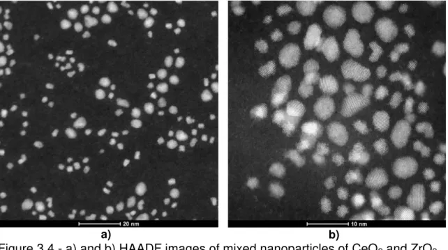
Figure 3.5 - a) and b) HAADF images of mixed nanoparticles of CeO2 and ZrO2... 50
Figure 3.6 - a) EDX image mapping of mixed nanoparticles of CeO2 and ZrO2, and b) EDX spectrum of the scanned area. ... 51
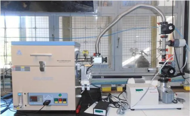
Figure 3.7 - MTI furnace with quartz tube, and T-Station 75D turbomolecular pump. ... 52
Figure 3.8 - Heat treatment curve used to remove the organic layer. Green line and red line are the set temperature, and real temperature respectively. ... 53
Figure 3.9 - Low magnification HRTEM images of mixed nanoparticles (CeO2 and ZrO2): a) before, and b) after the remotion of the organic layer. ... 53
Figure 3.10 - TEM grids, a) metal grid with carbon support film, b) metal grid with lacey support film, c) silicon grid with membrane, and d) cross section of c). a) and b) from https://emresolutions.com; c) from http://www.octalab.com; d) from https://www.temwindows.com. ... 55
Figure 3.11 - Micrograph of: a) holey carbon film, and b) lacey carbon film. From https://emresolutions.com ... 56
Figure 3.12 – a) E-chip device featuring a ceramic membrane used for heating. b) Schematic top view of the heater chip. The insets are low-magnification TEM images of the central region of the chip showing the pattern of holes in the low-conductivity ceramic membrane and holey carbon support film overlaying the holes in the ceramic membrane. c) Cross-section view of the chip shown in b). (Courtesy of Protochips Inc.). ... 57
Figure 3.13 - a) Gatan 628 single tilt heating holder, and b) SmartSet Hot Stage controller. ... 58
Figure 4.1 - XRD pattern of the samples synthesized by the hydrothermal methodology, (a) synthesized on the laboratory, and (b) reported on the literature. ... 59
Figure 4.3 - a), b) TEM images, and c), d) particles size distribution of cerium nanoparticles reported by Cordeiro et al. [70]. ... 60
Figure 4.4 - Thermal cycles of the different tests of solvent-controlled syntheses. ... 63
Figure 4.5 - Dispersions of the different syntheses made by the solvent-controlled method using hydrated precursors. ... 63
Figure 4.6 – Low magnification HRTEM images of ceria synthesis made by the solvent-controlled method; samples (a) CeO2 acec(3_2), (b) CeO2 acec(5), (c) CeO2 acec(6), and (d) CeO2 acec(8_2). ... 64
Figure 4.7 - Dispersion of the different synthesis made by the solvent-controlled method using previously dehydrated precursors; from left to right the samples has 0, 1, 3, and 5 mmol of OAm respectively ... 65
Figure 4.8 - TEM images and particle size distribution of ceria nanoparticles synthesized with, 0 a) and b), 1 c) and d), 3 e) and f), and 5 mmol of OAm. ... 67
Figure 4.9 - XRD patterns of ceria nanoparticles synthesized with 0, 1 and 3 mmol of OAm. ... 68
Figure 4.10 - TGA of ceria nanoparticles synthesized with 0, 1 and 3 mmol of OAm. ... 68
Figure 4.11 - UV-Visible spectrum of ceria nanoparticles synthesized with 0, 1 and 3 mmol of OAm. ... 69
Figure 4.12 - HRTEM images and the corresponding FFT of ceria nanoparticles synthesized with, 0 a) and b), 1 c) and d), 3 mmol of OAm e), f), g), and h). ... 70
Figure 4.13 - Low magnification HRTEM images and the corresponding FFT of ceria nanoparticles synthesized with, 0 a) and b), 3 mmol of OAm c) and d). ... 71
Figure 4.14 - a) CeO2 with fluorite structure oriented in the zone axis
[101], b) multislice image simulation for the experimental image conditions, and c) HRTEM image of CeO2 nanoparticle, inset, the red lines indicate the HRTEM multislice simulation. ... 72
Figure 4.16 – a) Representation of the unit cell of CeO2 (Fluorite), b) and c) (110) plane. ... 74
Figure 4.17 - Superimposition of simulated 3D crystals over HRTEM images. Isolated nanoparticles of ceria synthesized with a), b), and c) 1, and d), e), and f) 3 mmol of OAm. ... 75
Figure 4.16 - Simulated assembly of ceria nanoparticles; oriented assembly on the crystallographic plane a) {110}, b) {111}, and c) {100}. ... 76
Figure 4.17 - Two possible growth mechanisms of the CeO2 cube-like NCs [70]. ... 76
Figure 4.20 - XRD patterns of zirconia nanoparticles before (benzyl alcohol) and after (oleic acid) the change of the organic layer. ... 78
Figure 4.21 – Low magnification HRTEM images of zirconia nanoparticles; a) before, and b) after the change of the organic layer. c) Particle size distribution after the change of the organic layer... 78
Figure 4.22 – a) HRTEM image, and b) EDS of the zirconia nanoparticles after the change of the organic layer. ... 79
Figure 4.23 - TGA of zirconia nanoparticles after the change of the organic layer. ... 79
Figure 4.24 - Dispersion of zirconia nanoparticles after the change of the organic layer... 80
Figure 4.23 - Low magnification HRTEM image of mixed nanoparticles (CeO2 and ZrO2) after an ex situ test at 300°C for 2 hours. ... 81
Figure 4.24 - a) Silicon nitride TEM 9 windows grid with 5 nm thick square membrane, and b) drop of the dilution of mixed oxides over the TEM grid. ... 81
Figure 4.27 - Low magnification HRTEM images of ex situ test at 500°C for 30 minutes in mixed nanoparticles of CeO2 and ZrO2. ... 82
Figure 4.28 - Low magnification HRTEM images of ex situ test at 600°C for 30 minutes in mixed nanoparticles of CeO2 and ZrO2. ... 83
Figure 4.30 - Low magnification HRTEM images of ex situ test at 600°C for 60 minutes in mixed nanoparticles of CeO2 and ZrO2. ... 85
Figure 4.31 - HRTEM image of ex situ test at 600°C for 60 minutes. Inset FFT of some ceria nanoparticles in oriented attachment. ... 85
Figure 4.32 - Particle size distribution of CeO2 and ZrO2 a) before, and b) after ex situ test at 600°C for 60 minutes. ... 86
Figure 4.31 - Low magnification HRTEM images of ZrO2 nanoparticles at room temperature exposed to an EBCD of 5000 A/m2 for: a) 0 min, b) 30 min, and c) 60 min. ... 86
Figure 4.32 - Low magnification HRTEM images of ZrO2 nanoparticles at room temperature exposed to an EBCD of 2000 A/m2 for: a) 0 min, b) 30 min, and c) 60 min. ... 87
Figure 4.33 - Low magnification HRTEM images of ZrO2 nanoparticles at room temperature exposed to an EBCD of 1000 A/m2 for: a) 0 min, b) 30 min, and c) 60 min. ... 87
Figure 4.34 - Low magnification HRTEM images of ZrO2 nanoparticles at room temperature exposed to an EBCD of 800 A/m2 for: a) 0 min, b) 30 min, and c) 60 min. ... 87
Figure 4.35 - Zoom of Figure 4.37, highlighting some ZrO2 nanoparticles at room temperature exposed to an EBCD of 2000 A/m2 for: a) 0 min, b) 30 min, and c) 60 min. ... 89
Figure 4.36 - Change in the projected area of the nanoparticles shown in Figure 4.40. ... 90
Figure 4.37 - Low magnification HRTEM images of mixed nanoparticles (CeO2 and ZrO2), a) 800°C for 0 min, b) 800°C for 90 min, c) 800°C for 90 min + 900°C for 120 min, and d) 800°C for 90 min + 900°C for 120 min + 950°C for 30 min. ... 92
Figure 4.40 - HRTEM image at room temperature of some ZrO2 nanoparticles with the SmartSet Hot Stage controller turned on a), and off c); and his respective FFT b) and d). ... 94
Figure 4.43 - Low magnification HRTEM images of mixed nanoparticles (CeO2 and ZrO2), after 185°C for 5 hours in a furnace with air atmosphere, to remove the organic layer, and heated in situ at 800°C for: a) 0 min, b) 30 min, and c) 60 min. ... 95
Figure 4.44 - a) Subtraction of the Figure 4.42a and Figure 4.42c... 95 Figure 4.43 - TGA and DTG of: a) CeO2, and b) ZrO2 nanoparticles. ... 96 Figure 4.44 - Low magnification HRTEM images of ZrO2 nanoparticles, after 510°C for 5 hours in a furnace with air atmosphere, to remove the organic layer, and heated in situ at 800°C for 60 min + 950°C for 60 min + 1050°C for: a) 0 min, b) 90 min, and c) 180 min... 96
Figure 4.45 - Subtraction of the Figure 4.44a and Figure 4.44c. ... 97 Figure 4.46 - Particle size distribution of ZrO2 a) before, and b) after in situ heating at 800°C for 60 min + 950°C for 60 min + 1050°C for 180 min. ... 98
Figure 4.47 - Schematic representation of a CeO2 nanoparticle, without and with oxygen atoms on its surface. ... 98
Figure 4.48 - Low magnification HRTEM images of ZrO2 nanoparticles heated in situ at 500°C for 180 min at low EBCD plus: a) 0 min, b) 60 min, c) 120 min, and d) 240 min at a higher EBCD. ... 100
Figure 4.49 - Low magnification HRTEM images of ZrO2 nanoparticles heated in situ at 500°C for: a) 0 min, and b) 420 min. ... 101
Figure 4.49 - Low magnification HRTEM images of mixed nanoparticles (CeO2 and ZrO2) heated in situ at 500°C for: a) 0 min, and b) 180, c) 240min, and d) 360 min. ... 102
Figure 4.50 - HRTEM images of mixed nanoparticles (CeO2 and ZrO2) heated in situ at 500°C for 360 min. ... 103
Figure 4.52 - Zoom of the areas marked with the white square in Figure 4.53a, and b respectively. ... 105
Figure 4.53 - Low magnification HRTEM images of mixed nanoparticles (CeO2 and ZrO2) heated in situ at 950°C for: a) 5, b) 30, c) 60, d) 180, e) 240, and f) 360 minutes. ... 106
Figure 4.54 - Low magnification HRTEM images of mixed nanoparticles (CeO2 and ZrO2) a) before, and b) after in situ heating at 950°C for 360 minutes. ... 107
Figure 4.55 - HRTEM images, and his respective FFT, of mixed nanoparticles (CeO2 and ZrO2) before a) and b), and after c) and d) in situ heating at 950°C for 360 minutes. ... 108
Figure 4.56 - HRTEM images of mixed nanoparticles (CeO2 and ZrO2) after in situ heating at 950°C for 360 minutes. ... 109
Figure 4.57 - Schematic representation of a liquid cell design that can be introduced inside a TEM [58]. ... 111
Figure 4.58 - Sintering of CeO2 nanoparticles at 890°C in vacuum. a) 2 min, b) 7 min, c) 11 min, d) 18 min, e) 31 min and f) 38 min [88]. ... 113
Figure 4.59 - Zoom of Figure 4.60f. The area highlighted in red indicates a region of the carbon film that was removed due to beam damage. Adapted from [88] ... 114
Figure 4.60 - Sintering of CeO2 nanoparticles at 890°C in vacuum. a) 11 min, b) 18 min; c) and d) zoom of a) and b) respectively. Adapted from [88]. 115
Figure 4.60 - Low magnification HRTEM images of in situ experiment of pure γ-Fe2O3, a) before and b) after heating at 750°C [79]. ... 116
Figure 4.61 - Low magnification HRTEM images of in situ experiment of Sn doped γ-Fe2O3, a) before and b) after heating at 750°C [79]. ... 117
Figure 4.62 - Particle size distribution of: a) γ-Fe2O3 before, b) Sn doped γ-Fe2O3 after, and c) γ-Fe2O3 undoped after in situ heating experiments at 750°C [79]... 117
Figure 4.64 - Sequence of HRTEM images for Sn doped γ-Fe2O3 treated at 750°C. Adapted from [79]. ... 119
Figure 4.65 - 3D simulation of ceria nanoparticles, comparing two nanoparticles with a mean size 2.7 nm and 12 nm. ... 120
Figure A. 1 - Assembly for synthesis of tin oxide nanoparticles. ... 137 Figure A.2 - Dispersion of tin oxide nanoparticles synthesized by the solvothermal method. ... 138
Figure A.3 - XRD of tin oxide nanoparticles synthesized by the solvothermal method. ... 138
Figure A.4 - a) Low magnification HRTEM image of tin oxide nanoparticles, b) HRTEM image of isolated particles. c) Particle size distribution. ... 139
Figure A.5 - TGA of tin oxide nanoparticles synthesized by the solvothermal method. ... 140
Figure B.1 - Low magnification HRTEM images and the corresponding FFT of ceria nanoparticles synthesized with, 0 mmol of OAm... 141
Figure B.2 - Low magnification HRTEM images and the corresponding FFT of ceria nanoparticles synthesized with, 3 mmol of OAm... 142
Figure B.3 - Low magnification HRTEM images before and after the ex situ test at 500°C for 30 minutes in mixed nanoparticles of CeO2 and ZrO2. ... 143
Figure B.4 - Low magnification HRTEM images before and after the ex situ test at 600°C for 30 minutes in mixed nanoparticles of CeO2 and ZrO2. ... 144
Figure B.5 - Low magnification HRTEM images before and after the ex situ test at 600°C for 60 minutes in mixed nanoparticles of CeO2 and ZrO2. ... 145
Figure B.6 - HRTEM images and his respective FFT, of mixed nanoparticles (CeO2 and ZrO2) before in situ heating at 950°C for 360 minutes. ... 146
SYMBOLS AND ABBREVIATIONS BF Bright-Field
BFP Back Focal Plane
BSE Backscattered Electrons
CBED Convergent Beam Electron Diffraction CCD Charge-Coupled Device
Ce(aca)3 Cerium(III) acetylacetonate
DF Dark-Field
DPs Diffraction Patterns
DTA Differential Thermal Analysis DTG Derivative Thermogravimetry EBCD Electron Beam Current Density
EDX, EDS or EDXS Energy-Dispersive X-Ray Spectroscopy EELS Electron Energy Loss Spectroscopy
EM Electron Microscope (or Microscopy)
ETEM Environmental Transmission Electron Microscope (or Microscopy)
FEG Field Emission electron Gun FFT or FT (fast) Fourier Transform FTIR Fourier Transform Infrared FWHM Full Width at Half Maximum HAADF High-Angle Annular Dark Field
HRTEM High-Resolution Electron Microscope (or Microscopy) JCPDS Joint Committee on Powder Diffraction Standards LED Light Emission Diode
MEMS Microelectromechanical Systems mt metric tons
NCs nanocrystals OAc Oleic Acid OAm Oleylamine OLA Oleyl Alcohol
ppm Parts per million
rcf Relative Centrifugal Force REEs Rare Earths Elements ROS Reactive Oxygen Species rpm Revolutions per minute
SAD or SAED Selected-Area (electron) Diffraction SE Secondary Electrons
SEM Scanning Electron Microscope (or Microscopy) SNR Signal-to Noise Ratio
STEM Scanning Transmission Electron Microscope (or Microscopy)
TEM Transmission Electron Microscope (or Microscopy) TG Thermogravimetry
TGA Thermogravimetric Analysis or Thermal Gravimetric Analysis
THF Tetrahydrofuran TWC Three-Way Catalysis USD United State Dollar UV Ultraviolet
XRD X-Ray Diffraction
Z atomic (or proton) number
alfa
beta
γ gamma
delta
micron
λ lambda
physicist Ernst Ruska and the electrical engineer Max Knoll in Berlin in 1931. In 1986, shortly before his death, Ruska received the Nobel Prize “for his fundamental work in electron optics, and for the design of the first electron microscope”. Moreover, Reinhold Rudenberg, the scientific director of Siemens-Schuckertwerke, obtained the patent for the electron microscope in May 1931. In 1930 the 2 ¾ year-old son of Rudenberg became ill with leg paralysis, the illness was diagnosed as poliomyelitis, known to be caused by a virus. This encourages Rudenberg to find a way to make such a small virus visible, because they are too small to be detected under an optical microscope.
In 1933 Ruska build an electron microscope that exceeded the resolution attainable with an optical microscope, but it was only until 1938 that the first commercial electron microscope was produced by Siemens. After years of development in the lenses and detectors, in 1965 the Cambridge Scientific Instrument Company finally let to the market the first commercial Scanning Electron Microscope (SEM) named “Stereoscan”. While in 1965 the scanning microscopy was barely born, in the 1960s and 1970s the first megavolt Transmission Electron Microscopes (TEM) was developed. These instruments had sufficient space in their specimen stages to accommodate heating, tensile and gas-reaction stages, and also were powerful enough to permit observation of specimens that were thick enough to mimic bulk behavior.
experiments can be conducted in real time inside the specimen chamber of electron microscopes [2,3]. This field of experimentation became known as in situ electron microscopy. In recent years, in situ TEM techniques were developed by introducing various attachments, such as gas, force, electricity, heat, and so on [4]. A stage designed to heat specimens up to high temperatures in the microscope allow us to observe phase transformation, change in the oxidation states or reactions between nanostructures at atomic level.
“We live in a society exquisitely dependent on science and technology, in which hardly anyone knows anything about science and technology.”
- Carl Sagan
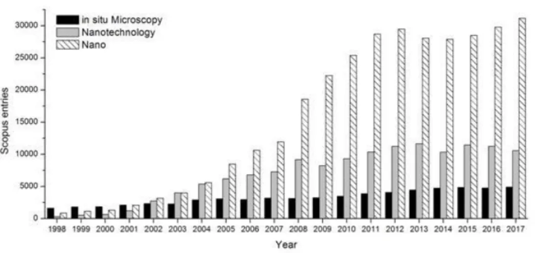
The same quote by Carl Sagan can be applied to nanotechnology. In the last two decades, the number of scientific articles related to the terms “nano” or “nanotechnology” has increased from a few to tens of thousands (Figure 1.1), according to a search made on Scopus. Today we use nanotechnology in many products of our daily lives, from microprocessors, electronics and medicine to cosmetics and textiles. New properties, applications, related to nano-scale products are discovered every day.
Since the beginning of humanity, man has had the ability to master new technologies, even without understanding them. 1.5 million years ago, Homo erectus used fire even before knowing how to create it. In ancient times, silver was used to serve beverages intended for monarchs and aristocrats; its antiseptic properties were known thousands of years before the invention of the optical microscope and identification of bacteria and other microorganisms. Nowadays we use silver nanoparticles to increase their bactericidal properties.
It is obvious that a better understanding of the phenomena that occur on at nanoscale will allow us to enhance the already known properties and applications, and maybe discover some new ones. This is why the in situ electron microscopy is so important, since it allow us to observe these phenomena in real time.
Even with in situ microscopy, reproduce the exact phenomenon is difficult, since the conditions of vacuum and high electron radiation to which the sample is exposed inside the microscope can alter its normal behavior. Another problem is the lack of reproducibility, which makes difficult the comparison between the obtained results and others reported in the literature. Two-thirds of researchers who responded to a survey by the journal Nature said that current levels of reproducibility are a major problem. Pressure to publish, selective reporting, poor use of statistics and finicky protocols can all contribute to wobbly work [5].
2 LITERATURE REVIEW
2.1 A brief summary of Cerium, Zirconium, and Tin oxide
In 2010 the global production of rare earths elements (REEs) was 133600 metric tons (mt). Cerium was the highest consumed elements accounting for over 39% of global consumption in 2012 [6], for this year the global REEs market was valued at USD 4.3 billion and is expected to reach USD 10.9 billion by 2020; being the catalysts one of the dominant applications. United States major end uses for REEs include automotive catalytic converters and fluid cracking catalysts in petroleum refining with about 60% of the local consumption [7].
Brazil is the fourth worldwide producer of REEs, although China has a monopoly with around 96.9% of the total production [7]; New technological knowledge in the extraction and production of REEs are under development, but it is not enough because for be at the forefront with these strategic minerals it is imperative a full understanding of all the aspects around their performance. As Senator Luiz Henrique said, “Brazil cannot once again make the same mistake we made in the 30s and 50s, when it became exporter of radioactive ores and denied to master nuclear technology” [8].
Cerium is the most abundant member of the series of elements known as lanthanides or REEs, ranked 26 with 66 ppm just above the Zinc and Cooper with 76 ppm and 68 ppm respectively [9]. Its high abundance, combined with excellent catalytic activity for a variety of reactions, makes cerium the element of choice. Cerium is characterized chemically by having two stable valence states, Ce+4, ceric and Ce+3, cerous. The ceric ion is a powerful oxidizing agent but when associated with oxygen is completely stabilized and indeed cerium oxide, Ce4+O2, (also called ceria) is the form of cerium most widely used.
Most of the catalytic traits can be attributed to two properties of ceria: first, the high mobility and storage capacity of oxygen within the lattice; second, the ease with which cerium changes between Ce3+ and Ce4+ states. These properties, combined with the abundance of cerium on earth, make ceria a low-cost highly effective alternative to noble metal catalysts. Recent research has been focused on the nanoscale properties of ceria [15], shown that nanostructured CeO2 gives a superior performance to bulk CeO2 when they are used as either catalyst or support [16].
On the bulk, when a O vacancy is created, two of the adjacent Ce cations change from Ce+4 to Ce+3. In nanoparticles, various studies has shown that decreasing the particle size increase the Ce+3/Ce+4 ratio [17–19]. Due to these change on the oxidation states ceria become the focus of attention, since satisfactory results have been reported in antibacterial [20], antioxidant [21–23], and biological applications. On the later, ceria can act as radical scavenging and protect the cells against reactive oxygen species (ROS) [19,21,24], on in vitro and in vivo tests ceria appear as a promising therapeutics for neuronal degenerative disorders [22,23,25]. To be successfully applied in biology nanoparticles should combine the properties of solids with the mobility of the molecules, besides of being stable and not agglomerate. Hence the value of synthesize small size particles with large surfaces that can interact with biological systems.
Zirconium oxide (ZrO2) known as zirconia is also a relevant material in electronic ceramics and catalysis. Zirconia is an extremely versatile ceramic with superior chemical stability, mechanical strength and ion-exchange capacity that has found use in oxygen sensors, fuel cells, thermal barrier coatings, and other high-temperature applications [26,27].
addition, the effect of the preparation method is also important; Devaraju et al. compared the solvothermal and co-precipitation calcinations methods, showing that the latter has a greater oxygen storage capacity (OSC) [33].
Moreover, Tin oxide (SnO2) based nanomaterials have received interest for use in gas/chemical sensor, transparent conductive electronics, electronic devices such as logic gates and computing circuits [37–39] and recently to fabricate ultraviolet light emission diodes (UV LEDs) [40]. Some studies have exposed the benefits of the addition of CeO2 to SnO2, showing an enhance in the thermal stability and catalysis activity for CO and CH4 oxidation [41], as well as the selectivity to CO compared to CH4 as a gas sensor [42]. Also, adding SnO2 to CeO2 shows more catalytic CO oxidation [43].
Parenthesis
Throughout this text the word surface will be used arbitrarily. At macro and
microscopic scale, a surface can be defined as the interface between the matter and its environment, either air, material, or vacuum; and this interface have a thickness (which most times is greater than the diameter of the nanoparticles that will be studied in this text). At atomic scale, we will call “surface”, the last layer of atoms on our particles,
film, etc.
2.2 Phase diagrams and solubility
The first contribution to the ceria-zirconia system was made by L. Passerini in 1930. Due the importance of this system even in the last decade still made research and contributions to this phase diagram [44–46]. Several studies found a different compound form of tetragonal zirconia or fluorite ceria, with 40mol % CeO2 (Ce0.4Zr0.6O2) who is stable below 870°C after long periods of annealed in bulk oxides. It is worth to highlight that for these bulk oxides around 1000°C and between 20-80 mol % of CeO2 have a combination of tetragonal and fluorite phases, while in nanostructures for the same range only the fluorite structure is present, this is an example that the materials can behave in unusual ways when are in nanoscale. Figure 2.1 shows a tentative phase diagram for the CeO2-ZrO2 system, developed experimentally [45].
cubic CeO2 at 1250°C is 30 mole percent (in the bulk) [46]. While in the nano size, the solid solution of ZrO2 in fluorite phase of CeO2 nanoparticles can be as high as 40 mole percent at room temperature [47]. The increase of the solubility of an element in small particles (nano) is already well known for years [48], but this approach is merely theoretical and no information was found in the literature for such small size as the evaluated in this work. Also, even though both elements (Ce, and Zr) have high solubility there is no guarantee that the particles of the two species will react with each other to form a new particle of homogeneous composition.
For the CeO2-SnO2 system no phase diagram was found, but some works gives an idea of the solubility of an oxide in the other. Ayastuy et al. estimated the limit of solubility of tin into ceria lattice (fluorite) as 22mol %, but it is possible to see a small peak of SnO2 at 15mol% (Figure 2.2a) in their XRD which infers that the solubility is between 10-15mol % [43]. Instead, when the cerium is the dopant can enters the lattice of SnO2 to form solid-solution up to 33mol % without segregation of CeO2 [41]. Observing the result of Xu et al. it is appreciated an increase of the Full Width at Half Maximum (FWHM) in the ceria doped tin oxide, and also no peak of ceria appears (Figure 2.2b), which demonstrates a variation in the lattice parameters due to non-uniform strain induced by the substitutional cerium in solid solution.
Figure 2.2 - a) XRD patterns of CeO2-SnO2 mixed oxides, variation from 0 to 0.20 mol % of tin oxide [43], and b) comparison of the two pure oxides with a mixture with Sn/Ce atomic ratio of 2:1 corresponding to 33mol % of CeO2 [41]. The red arrows in (a) indicate the appearance of tin oxide at 15mol %; in (b) shows an increase of the Full Width at Half Maximum of tin oxide due to cerium in solid solution at 33mol %.
2.3 Conceptual Framework 2.3.1 Electron microscope
A microscope is an instrument that increases resolution over that of the human eye alone (about 150 μm between two points or lines). An electron microscope is a microscope that uses a beam of accelerated electrons as a source of illumination. The two main types of electron microscopes are: scanning and transmission. A scanning electron microscope (SEM) scans a focused electron beam over a surface to create an image. The electrons in the beam interact with the sample, producing various signals, and the reflected electrons can be used to obtain information about the surface topography and composition. In a transmission electron microscope (TEM) the electron beam is transmitted through a specimen to form an image. The word "transmission" suggests that the sample must be fine enough for the electrons to pass through it (usually less than less than 100 nm thick).
Microscopy is the interpretive use of microscopes. No matter what kind of microscope, employing whatever medium, manner, or kind of specimen, microscopy also requires a primary observer to interpret the image.
Resolution is the distance between two specific points or parts of the object as viewed by the eye, microscope, camera, or video. Resolving power is the ability to distinguish two points of an object as separate in an image (with their diffraction discs not overlapping more than half their diameters). The resolving power is expressed theoretically as the minimum distance between two adjacent, separated points; resolution is the actual perception of the two separate points. Practical resolution needs adequate contrast [49].
maximum) surrounded by concentric 1st, 2nd, 3rd, etc., order maxima of sequentially decreasing brightness that make up the intensity distribution. Two Airy disks and their intensity distributions at the limit of optical resolution are illustrated in Figure 2.3b. In this part of the figure, the separation between the two disks exceeds their radii, and they are resolvable. The limit at which two Airy disks can be resolved into separate entities is often called the Rayleigh criterion; which is extensively used to determine the resolution of microscopes. Figure 2.3c shows two Airy disks and their intensity distributions in a situation where the center-to-center distance between the zeroth order maxima is less than the width of these maxima, and the two disks are not individually resolvable by the Rayleigh criterion.
Figure 2.3 - Airy disks and their intensity distributions as a function of separation distance. From Olympus America, Inc.
2.3.1.1 Interactions of electrons with matter
When a high-energy beam of electrons interacts with a thin specimen a wide range of secondary signals are produced. There are two types of interactions: elastic and inelastic. One of the main signals produced by elastic interactions is the elastically scattered electrons, which is the major source of contrast in TEM images, also creates much of the intensity in diffraction patterns (DPs). The inelastic interactions are equally important since they generate a whole range of signals, each of which can tell us more about the chemistry of the specimen than we can find out from the elastic electrons. Some of the most important signals are the electron energy-loss, the characteristic X-rays, secondary electrons, and, occasionally, visible light (cathodoluminescence).
Figure 2.4 - Signals generated when a high-energy beam of electrons interact with a thin specimen [1].
2.3.1.2 Electron beam damage
damage represents a real physical limit on what the TEM can do and may be regarded as the microscopists’ analog of the Heisenberg uncertainty principle in that the very act of observing your specimen can change it [1].
On the other hand, sometimes we can use beam damage to aid certain in-situ transformations that are speeded up by the damage process or we can use electron damage to emulate other forms of radiation damage. Generally, however, beam damage must be considered undesirable. Damage takes one of three principal forms [1,50]:
Radiolysis: Inelastic scattering (mainly electron-electron interactions such as ionization) breaks the chemical bonds of certain materials such as polymers and alkali halides. The excitation needs to be localized for a time long enough for the atom to respond mechanically, and the energy acquired by the excited atom must be convertible into momentum, resulting in atomic displacements.
Knock-on damage or sputtering: Knock-on damage is the displacement of atoms from the crystal lattice and creates point defects. These processes are ubiquitous if the beam energy (E0) is high enough. If the kinetic energy acquired by an atom is higher than its displacement threshold energy (Ed) or surface binding energy (Es), the atom may be displaced from its site to an interstitial or vacancy, forming a Frenkel pair in the bulk, or sputtered away from surfaces into vacuum. In TEM/STEM, the surface sputtering process usually dominates the former one, because Es is usually much smaller than Ed.
Heating: Phonons heat your specimen and heat is a major source of damage to polymers and biological tissue.
Other important mechanism is electrostatic charging of materials induced by the incident electron beam. Unlike scanning electron microscopy (SEM), charging in TEM/STEM is mainly caused by the ejection of secondary and Auger electrons into vacuum.
is only a small portion of the total energy carried by the incident beam. Therefore, it is more convenient to use the number of incident electrons during an exposure (the flow in C/cm2 or e/nm2), as the “electron dose”, to represent the strength of irradiation in TEM/STEM.
In the literature, this “dose” is defined as the product of electron current density (dose rate) and illumination (or exposure) time (A/m2 or e/nm2 s). Generally, it has been considered that there is a “dose threshold”, also known as the “critical dose” or ‘‘characteristic dose’’, for each beam-sensitive material, below which beam damage is negligible. The well-known low-dose technique commonly used for biological materials is based on this idea. For a given total dose there are two ways to achieve a low-dose condition in TEM/STEM: either by lowering the electron current density (dose rate) or by shortening the exposure time. The former is widely used in the low-dose technique, but the disadvantage is its low signal-to-noise ratio (SNR) and poor resolution. The latter may increase the SNR, but the very short acquisition time may induce artifacts due to the finite detector response time. Differences in image quality for the same dose but different exposure times (dose rate effects) are known as “reciprocity failure” [50].
1𝐴 1𝑚2×
1𝐶/𝑠 1𝐴 ×
6.242𝑥1018 𝑒
1𝐶 ×
1𝑚2
1𝑥1018 𝑛𝑚2 =
6.242 𝑒 𝑛𝑚2∙ 𝑠
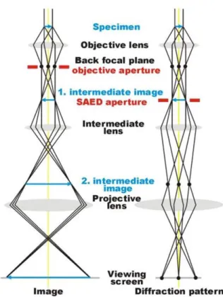
2.3.1.3 The Transmission Electron Microscope
magnified for viewing and recording. (3) The imaging system uses several lenses to magnify the image or the DP produced by the objective lens and to focus these on the viewing screen or computer display via a detector, CCD, or TV camera. The main components of a typical TEM are shown in Figure 2.5.
Below, a brief description of the main components:
Electron gun: The electrons are generated in the source and accelerated to the required energy; to be transferred to the sample.
Condenser system: A set-up of different magnetic lenses and apertures makes it possible to get either a parallel beam (micro probe for TEM image and selected-area diffraction, SAD) or a convergent beam with selected convergence angles (nano probe for STEM and convergent beam electron diffraction, CBED). Furthermore, the beam can be scanned (STEM) or tilted (DF-TEM).
Objective lens: Most important lens in the microscope since it generates the first intermediate image, the quality of which determines the resolution of the final image.
Diffraction/intermediate lens: Switching between imaging and diffraction mode.
Projective lenses: Further magnification of second intermediate image (image or diffraction pattern, respectively).
Image observation: Images and diffraction pattern can directly be observed on the viewing screen in the projection chamber or via a TV camera mounted below the microscope column. Images can be recorded on negative films, on slow-scan CCD cameras or on imaging plates.
Vacuum system: Because of strong interactions of electron with matter, gas particles must be absent in the column. The required high vacuum is maintained by a vacuum system typically comprising a rotary pump (pre-vacuum pump), a diffusion pump and one or more ion getter pumps.
Figure 2.6 - Ray diagram showing the two basic operation modes in TEM: Image mode, and Diffraction mode. From http://www.microscopy.ethz.ch
In imaging mode, an objective aperture can be inserted in the back focal plane to select one or more beams that contribute to the final image (Bright-Field (BF), Dark-(Bright-Field (DF), High-Resolution TEM (HRTEM)). For selected area electron diffraction (SAED), an aperture in the plane of the first intermediate image defines the region of which the diffraction is obtained. Ray diagrams, and comparison images, showing how the objective aperture is used to produce BF, DF and HRTEM images are shown in Figure 2.7.
Figure 2.7 - Ray diagram showing how objective aperture is used to produce (a) BF, (b) DF, and (c) HRTEM images. Adapted from
http://www.microscopy.ethz.ch
In DF mode, the direct beam is blocked by the aperture while one or more diffracted beams are allowed to pass the objective aperture (Figure 2.7b). Since diffracted beams have strongly interacted with the specimen, very useful information is present in DF images, e.g., about planar defects, stacking faults or particle size.
To obtain lattice images, a large objective aperture has to be selected that allows many beams including the direct beam to pass. The image is formed by the interference of the diffracted beams with the direct beam (phase contrast). If the point resolution of the microscope is sufficiently high and a suitable crystalline sample oriented along a zone axis, then HRTEM images are obtained (Figure 2.7c).
2.3.1.4 Fast Fourier transforms of images
transform is a mathematical method for transforming a function of time (or space) into a function of frequency (or reciprocal space).
We can also think of an image as a varying function, however, rather than varying in time it varies across the two-dimensional space of the image. In a grey scale digital image the pixels each have a value between 0 and 255 representing the darkness of that pixel. So the darkness, or intensity, of that pixel, is a function of the horizontal and vertical coordinates giving the location of that pixel. We can think of the image as an undulating landscape, with the height of the landscape given by the value of the pixel. Figure 2.8 shows a black and white digital photograph and the image function of the same digital photograph, with the gray value u(x, y) plotted as the height of the surface over the (x, y)-plane.
Figure 2.8 - Black and white digital photograph and its representation as a function of gray intensity. From https://plus.maths.org
As we showed earlier, the formation of an HRTEM image requires the use of an aperture large enough to include both the transmitted beam and at least one diffraction beam, in which the transmitted beam provides a reference phase of the electron wavefront. As a result, HRTEM images are interference patterns between the transmitted and diffracted electron waves from the specimen.
the atom cores, and channels along the atom columns of the crystallographic lattice. At the same time, the interaction between the electron wave in different atom columns leads to diffraction. This is known as Fraunhofer diffraction; since a plane incident wave was considered and the diffraction pattern is observed at an infinite distance. Since a wave emitted by a point (atom) becomes planar at large distances.
To change the observation plane of the diffraction pattern from infinite to the back focal plane, a lens is used. So the objective lens in a TEM performs as a Fourier transform.
Figure 2.9 - Ray diagram showing the formation of a TEM image. From http://www.microscopy.ethz.ch
This means that the electron wavefunction in the image plane is the same (multiplied by a contrast transfer function) as in the exit of the crystal.
Since the digital gray image obtained in the image plane is a replica of the crystal, we can repeat the previous process; this time not with lens, but using a mathematical tool in the image function, i.e. applying a fast Fourier transform (FFT) to the image to reveal the diffraction pattern. Figure 2.10 and Figure 2.11 are an example of how, when the necessary conditions are met (a crystalline sample oriented in the zone axis, among others), the selected area electron diffraction (SAED) and the FFT are equivalent.
Figure 2.10 - (a) SAED, (b) Low magnification HRTEM image, and (c) FFT of b), of crystalline biogenic calcite. From [51]
Thus, in a crystalline sample oriented in the zone axis, the intensity distribution in a HRTEM image corresponds to the electron density distribution, which is stronger at the atomic columns positions. This means that we are visualizing the crystal structure in the real space. From this we can directly measure the lattice spacing, or apply a FFT to identify patterns of symmetrically organized atoms, i.e. crystallographic planes.
It is worth noting that, as the spots on the FFT come from a mathematical treatment to an image, and not from a diffraction phenomenon, some artifacts in the image that are not directly related with the diffraction process itself (like electromagnetic noise in the microscope, noise in the CCD camera, among others) can generate other spots that are not related with a satisfied diffraction condition in a crystalline sample.
Summarizing, the FFT of a HRTEM image is a powerful tool that, like the SAED, help us to characterize, and analyze the crystal structures and crystal defects of our samples; like lattice matching, interfaces, twinning, among others.
2.3.2 Nanoparticle synthesis
“Nanoparticle synthesis refers to methods for creating nanoparticles. Nanoparticles can be derived from larger molecules, or synthesized by ‘bottom -up’ methods that, for example, nucleate and grow particles from fine molecular distributions in liquid or vapour phase. Synthesis can also include functionalization by conjugation to bioactive molecules.” Nature.com
2.3.2.1 Coprecipitation
Coprecipitation is the simultaneous precipitation of a normally soluble component with a macro-component from the same solution by the formation of mixed crystals, by adsorption, occlusion or mechanical entrapment. An adsorbate is an impurity that is weakly bound (adsorbed) to the surface of the precipitate. An occlusion occurs when an adsorbed impurity gets physically trapped inside the crystal as it grows. Coprecipitation reactions involve the simultaneous occurrence of nucleation, growth, coarsening, and/or agglomeration processes.
As a brief overview, coprecipitation reactions tend to exhibit the following characteristics: (i) The products of precipitation reactions are generally sparingly soluble species formed under conditions of high supersaturation. (ii) Such conditions dictate that nucleation will be a key step of the precipitation process and that a large number of small particles will be formed. (iii) Secondary processes, such as Ostwald ripening and aggregation, will dramatically affect the size, morphology, and properties of the products. (iv) The supersaturation conditions necessary to induce precipitation are usually the result of a chemical reaction [54].
2.3.2.2 Sol-Gel
The sol-gel process involves conversion of monomers into a colloidal solution (sol) that acts as the precursor for an integrated network (or gel) of either discrete particles or network polymers. Typical precursors are metal alkoxides.
The sol-gel process can be characterized by a series of distinct steps. Step 1: Formation of stable solutions of the alkoxide or solvated metal precursor (the sol).
Step 3: Aging of the gel (syneresis), during which the polycondensation reactions continue until the gel transforms into a solid mass, accompanied by contraction of the gel network and expulsion of solvent from the gel pores. Ostwald ripening and phase transformations may occur concurrently with syneresis. The aging process of gels can exceed 7 days and is critical to the prevention of cracks in gels that have been cast.
Step 4: Drying of the gel, when water and other volatile liquids are removed from the gel network. This process is complicated due to fundamental changes in the structure of the gel. The drying process has itself been broken into four distinct steps: (i) the constant rate period, (ii) the critical point, (iii) the first falling rate period, and (iv) the second falling rate period. If isolated by thermal evaporation, the resulting monolith is termed a xerogel. If the solvent is extracted under supercritical or near-supercritical conditions, the product is an aerogel.
Step 5: Dehydration, during which surface-bound M−OH groups are removed, thereby stabilizing the gel against rehydration. This is normally achieved by calcining the monolith at temperatures up to 800 °C.
Step 6: Densification and decomposition of the gels at high temperatures (T > 800 °C). The pores of the gel network are collapsed, and remaining organic species are volatilized. This step is normally reserved for the preparation of dense ceramics or glasses.
2.3.2.3 Hydrothermal and Solvothermal synthesis
Some solvothermal processes indeed involve supercritical solvents. Most, however, simply take advantage of the increased solubility and reactivity of metal pressures without bringing the solvent to its critical point. In any event, solvothermal processing allows many inorganic materials to be prepared at temperatures substantially below those required by traditional solid-state reactions. Unlike the cases of coprecipitation and sol-gel methods, which also allow for substantially reduced reaction temperatures, the products of solvothermal reactions are usually crystalline and do not require post-annealing treatments.
2.3.2.4 Solvent-Controlled Synthesis
The solvent-controlled synthesis is considered a simpler approach, compared to other synthesis process. The starting reaction mixture generally just consists of a metal oxide precursor and a common organic solvent, and on the other hand the synthesis temperature is lower, typically in the range of 50 to 200°C. However, without any doubts the main advantage of the solvent-controlled (or surfactant-free) synthesis methods lies in the improvement of product purity. Surface-adsorbed surfactants not only influence the toxicity of nanoparticles, but also lower the accessibility of the nanoparticle surface in catalytic and sensing applications.
In the solvent-directed approaches the organic solvent can act as reactant as well as controlling agent for particle growth and thus makes the use of surfactants superfluous. However, the detailed role of the organic species in these approaches is rather complex. On the one hand they provide the oxygen for the formation of the metal oxide, and on the other hand they act as capping agent, which binds to the particle surface, and thus limits the particle growth, and influences morphology and assembly behavior.
thereof, and the solvents range from oxygen-containing alcohols, ketones and aldehydes, to oxygen-free solvents like amines, acetonitriles or toluene [53].
The most frequently used reaction systems for metal oxide nanoparticle in non-aqueous and surfactant-free synthesis are:
i) reaction of metal halides with alcohols,
ii) metal alkoxides, acetates and acetylacetonates with alcohols, iii) metal alkoxides with ketones or aldehydes, and
iv) metal acetylacetonates with amines and nitriles
The reaction of metal halides, in general metal chlorides, with alcohols presumably represents the simplest non-aqueous approach to metal oxide nanoparticles, and it can, in the most cases, be performed by simple “beaker” chemistry using an oil bath as heating tool. Metal chlorides like FeCl3, VOCl3, CoCl2, WCl6, SnCl4, HfCl4, NbCl5, TaCl5 and TiCl4 readily react with various alcohols to the corresponding metal oxides. The metal halide - alcohol system with its low reaction temperature is particularly useful and versatile in cases where either surface functionalization of the nanoparticles with organic ligands is desired, or where biomimetic reaction principles based on the use of organic templates have to be applied in order to tailor crystal morphology.
The reaction of metal halides with alcohols almost always results in metal oxide nanoparticles with halide impurities. To avoid this contamination synthesis routes based on the reaction of metal acetates, acetylacetonates, or alkoxides with alcohols provide a halide-free alternative.
A detailed description of the chemical reaction mechanisms can be found elsewhere [53].
2.3.3 Solvents
1) (Non-participatory) to dissolve the reactants: Polar solvents are best for dissolving polar reactants (such as ions); nonpolar solvents are best for dissolving nonpolar reactants (such as hydrocarbons).
2) Participatory: as a source of acid (proton), base (removing protons), or as a nucleophile (donating a lone pair of electrons).
What does “polar” and “non-polar” mean?
Polar solvents have large dipole moments (“partial charges”); they contain bonds between atoms with very different electronegativities, such as oxygen and hydrogen.
Non polar solvents contain bonds between atoms with similar electronegativities, such as carbon and hydrogen (think hydrocarbons, such as gasoline). Bonds between atoms with similar electronegativities will lack partial charges; it’s this absence of charge which makes these molecules “non-polar”.
There are two common ways of measuring this polarity. One is through measuring a constant called “dielectric constant” or permitivity. The greater the dielectric constant, the greater the polarity (water = high, gasoline = low). A second comes from directly measuring the dipole moment.
There’s a final distinction to be made and it is a source of confusion. Some solvents are called “protic” and some are called “aprotic”.
Protic solvents have O-H or N-H bonds. Why is this important? Because protic solvents can participate in hydrogen bonding, which is a powerful intermolecular force. Additionally, these O-H or N-H bonds can serve as a source of protons (H+).
Aprotic solvents may have hydrogens on them somewhere, but they lack O-H or N-H bonds, and therefore cannot hydrogen bond with themselves.
Nonpolar solvents: These solvents have low dielectric constants (<5) and are not good solvents for charged species such as anions. However diethyl ether (Et2O) is a common solvent for Grignard reactions; its lone pairs are Lewis basic and can help to solvate the Mg cation.
“Borderline” Polar aprotic solvents: These solvents have moderately higher dielectric constants than the nonpolar solvents (between 5 and 20). Since they have intermediate polarity they are good “general purpose” solvents for a wide range of reactions. They are “aprotic” because they lack O-H or N-H bonds. For our purposes they don’t participate in reactions: they serve only as the medium.
Polar aprotic solvents: These solvents all have large dielectric constants (>20) and large dipole moments, but they do not participate in hydrogen bonding (no O-H or N-H bonds). Their high polarity allows them to dissolve charged species such as various anions used as nucleophiles (e.g. CN - , HO - , etc.). The lack of hydrogen bonding in the solvent means that these nucleophiles are relatively “free” in solution, making them more reactive. For general purposes these solvents do not participate in the reaction.
_________________________________________
__________________________________________
Figure 2.12 - Most common solvents. From https://www.masterorganicchemistry.com
2.4 Related works in in situ electron microscopy
Figure 2.13 - HREM image showing the process by which SiC is formed via solid-state reaction between Si and graphite at 1400°C [3].
Figure 2.14 - In situ TEM observation of rutile particle growth. The TEM micrographs show the absorption of the anatase particles into a rutile particle heated at (a) 710°C, (b) 800°C (0 min), (c) 800°C (31 min), (d) 800°C (160 min), (e) 800°C (211 min), and (f) after cooling [57].
shows a sequence of images from a movie showing typical dynamics of the attachment process.
Chao Zhu et al. fabricated their own liquid cell, by sandwiched a droplet of the solution into two TEM copper grids with formvar stabilized carbon support films face-to-face. They performed in situ tests at room temperature on oriented attachment of gold nanoparticles [59]. Alike Dongsheng Li et al.; Chao Zhu et al. report how gold nanoparticles rotate randomly and get closer, interacting until they share a common {111} orientation and a sudden contact occurs resulting in a oriented attachment. Figure 2.16 shows a sequence of images from a video, red lines stand for {111} facets and green ones for {100} facets. Dashed lines depict the relative angle between the {111} facets of the two particles. The direction of movement of the particles (approaching and rotation) is denoted by blue arrows.
![Figure 2.1 - Tentative phase diagram for the ZrO 2 -CeO 2 system, proposed by Duran et al [45]](https://thumb-eu.123doks.com/thumbv2/123dok_br/15926760.676346/40.892.219.635.453.1077/figure-tentative-phase-diagram-zro-ceo-proposed-duran.webp)

![Figure 2.13 - HREM image showing the process by which SiC is formed via solid-state reaction between Si and graphite at 1400°C [3]](https://thumb-eu.123doks.com/thumbv2/123dok_br/15926760.676346/63.892.274.659.144.654/figure-hrem-image-showing-process-formed-reaction-graphite.webp)
![Figure 2.16 - Imaging of oriented attachment at atomic level of gold nanoparticles. Scale bar 2 nm [59]](https://thumb-eu.123doks.com/thumbv2/123dok_br/15926760.676346/66.892.128.718.519.1086/figure-imaging-oriented-attachment-atomic-level-nanoparticles-scale.webp)
![Figure 2.19 - a)CeO 2 Nanocubes side size and the side ratio evolution: smaller nanocrystal; b) larger nanocrystal [68]](https://thumb-eu.123doks.com/thumbv2/123dok_br/15926760.676346/70.892.114.752.150.396/figure-nanocubes-ratio-evolution-smaller-nanocrystal-larger-nanocrystal.webp)