Critical role of a double-layer con
figuration
in solution-based unipolar resistive
switching memories
Emanuel Carlos , Asal Kiazadeh
1, Jonas Deuermeier,
Rita Branquinho , Rodrigo Martins
and Elvira Fortunato
1CENIMAT/i3N Departamento de Ciência dos Materiais, Faculdade de Ciências e Tecnologia (FCT), Universidade NOVA de Lisboa(UNL), and CEMOP/UNINOVA, 2829-516 Caparica, Portugal E-mail:a.kiazaden@fct.unl.ptandemf@fct.unl.pt
Received 4 April 2018, revised 27 May 2018 Accepted for publication 4 June 2018 Published DD MM 2018
Abstract
Lately resistive switching memories(ReRAM) have been attracting a lot of attention due to their possibilities of fast operation, lower power consumption, simple fabrication process and they can be scaled to very small dimensions. However, most of these ReRAM are produced by physical methods and nowadays the industry demands more simplicity typically associated with low cost manufacturing. As such, ReRAMs in this work are developed from a solution-based aluminum oxide(Al2O3) using a simple combustion synthesis process. The device performance is
optimized by two-stage deposition of the Al2O3film. The resistive switching properties of the
bilayer devices are reproducible with a yield of 100%. The ReRAM devices show unipolar resistive switching behavior with good endurance and retention time up to 105s at 85°C. The devices can be programmed in a multi-level cell operation mode by application of different reset voltages. Temperature analysis of various resistance states reveals afilamentary nature based on the oxygen vacancies. The optimizedfilm was stacked between ITO and indium zinc oxide, targeting a fully transparent device for applications on transparent System-On-Panel technology. Supplementary material for this article is availableonline
Keywords: solution combustion synthesis, resistive switching memory, transparent device, aluminum oxide(Al2O3)
(
SQ1 Somefigures may appear in colour only in the online journal) 1. Introduction
New materials and device concepts have been studied in the semiconductor industry to surpass various technological limitations[1–3]. Due to their high density and low fabrica-tion costs, the most prominent, non-volatile memories today areflash memory devices [1,4,5]. Nevertheless, these suffer from low endurance, low write speed, and high voltage requirements for write operations. In addition, the increasing density offlash is expected to run into physical limits, which is not compatible with the internet of things[4]. Taking that into account, a huge demand for fast, small and power
efficient memories has grown [1,4, 6,7]. Resistive random access memory(ReRAM) has attracted a renewed interest due to many advantages, including high switching speed, low power consumption and high density with a simple structure [6–8]. A ReRAM memory cell is a metal-insulator-metal (MIM) structure composed of a resistive switch medium, such as metal oxides, which could be easily integrated with existing CMOS technology[4,9]. Moreover, the high density mass storage could be supported by multi-level cell (MLC) operations in ReRAMs [10–12]. The resistive switching phenomenon has been observed in a wide variety of insulator oxides, such as Ta2O5, TiO2, HfO2, ZrO2and Al2O3[13–20].
The resistive switching in these materials occurs after an electroforming process known as dielectric soft breakdown.
Nanotechnology Nanotechnology 00(2018) 000000 (9pp)
1
Authors to whom any correspondence should be addressed.
Once defects reach a critical density, a template of ReRAM device is obtained. Partial rupture/formation of the conduct-ingfilament (CF) results in different resistance states.
Among these materials, Al2O3 is the most abundant
(noncritical raw material) and has promising resistive switching properties, as well as good breakdown field and good thermal stability [21, 22]. Aluminum oxide has been widely reported for use in resistive switching devices with various memory structures fabricated via different techniques such as ALD, thermal oxidation and sputtering [22–32]. According to the literature these structures with Al2O3show
unipolar and bipolar properties depending on the processing conditions [10, 22, 24, 27, 33]. Using a unipolar ReRAM array, the selector circuit structure could potentially be sim-plified with the integration of a diode and a unipolar ReRAM. Due to good scaling potential and ease of fabrication, applying a passive component is preferred[7,34]. It is widely accepted that the switching mechanism is the consequence of oxygen vacancies and oxygen ion formation in the Al2O3thin
film [27, 29, 31, 35–38]. Nevertheless, the conduction mechanism could change according to the resistance states[10].
Lately, solution-based memories have gained a lot of attention due to their low cost manufacturing, simplicity, comparable performance to those of high vacuum techniques, and good film uniformity in large areas [21,39, 40]. Inkjet printing, dip-coating and spin coating are the techniques most used for solution processing oxide semiconductors and insu-lators in memory applications[39,41–43]. However, only a few reports have been done on solution-based aluminum oxide memories, as depicted in table 1 [11, 23, 42]. Since 2011, combustion synthesis has been used to improve thin film transistor performance, however, until now it has not been applied to memory production[44]. In this synthesis an oxidizer(nitrates) and a fuel (urea, citric acid) are added to the precursor solution. During the annealing process an exother-mic reaction occurs, resulting in a reduction of the external heat required for the film formation; the removal of organic solvents and film densification lead to high-quality films [21,44].
In this work, we report for thefirst time solution-based unipolar aluminum oxide memories and study the influence of subsequent depositions using combustion synthesis(SCS) on the device performance. The ReRAM bilayer devices show unipolar resistive switching behavior with good endurance
and retention time of up to 105s at 85°C in vacuum, which surpass the state-of-the-art. Since transparent devices have attracted a lot of research interest in portable and consumer electronics such as flat panel displays, touch panels, optical sensors and smart windows, Al2O3films with the optimized
layer structure were stacked between transparent conductive oxide(TCOs) electrodes.
2. Experimental section 2.1. Precursor solution development
Aluminum nitrate nonahydrate(Al(NO3)3·9H2O, Fluka, 98%)
was dissolved in 2-methoxyethanol(2-ME, C3H8O2, ACROS
Organics, 99%), to yield a solution with an Al3+ ion con-centration of 0.2 M. The fuel (Urea, Sigma, 98%) was then added to the solution and maintained under constant stirring for 24 h. The urea to aluminum nitrate molar proportion was 2.5:1 in order to guarantee the redox stoichiometry of the reaction. The precursor solution wasfiltrated before use.
2.2. Film deposition and characterization
Prior to deposition, all substrates were cleaned as mentioned in a previous report [21]. Thin films were deposited by spin coating for 35 s at 2000 rpm(Laurell Technologies), forming a single (30 nm) and a bilayer (66 nm) of aluminum oxide. Each deposition was followed by an immediate annealing at 500°C on a hotplate for 30 min in air. Before the second layer deposition a 10 min UV/Ozone surface treatment was performed.
Optical properties were obtained using a Perkin Elmer lambda 950 UV/VIS/NIR spectrophotometer by measuring transmittance (T) in the wavelength range of 190–800 nm.
Thefilm structure was assessed by glancing angle x-ray diffraction(XRD) performed by an X’Pert PRO PANalytical powder diffractometer using Cu Kα line radiation (λ=1.540 598 Å) with an angle of incidence of the x-ray beam fixed at 0.9°. Fourier transform infra-red (FTIR) spectroscopy data of thin films deposited on Si substrates were recorded using an attenuated total reflectance (ATR) sampling accessory (Smart iTR) equipped with a single bounce diamond crystal on a Thermo Nicolet 6700
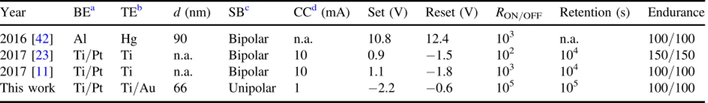
Table 1.Performance comparison of solution-based aluminum oxide ReRAM.
Year BEa TEb d(nm) SBc CCd(mA) Set(V) Reset(V) RON/OFF Retention(s) Endurance
2016[42] Al Hg 90 Bipolar n.a. 10.8 12.4 103 n.a. 100/100
2017[23] Ti/Pt Ti n.a. Bipolar 10 0.9 −1.5 102 104 150/150
2017[11] Ti/Pt Ti n.a. Bipolar 10 1.1 −1.8 103 104 100/100
This work Ti/Pt Ti/Au 66 Unipolar 1 −2.2 −0.6 105 105 100/100
a Bottom electrode. b Top electrode. c Switching behavior. d Current compliance.
Spectrometer. The spectra’s were acquired as reported in a previous article[21].
X-ray photoelectron spectroscopy (XPS) was measured with a Kratos Axis Supra, using monochromated Al Kα irradiation (1486.6 eV). The detail spectra were acquired under an emission angle of 90° with a pass energy of 5 eV, resulting in an energy resolution better than 0.45 eV. The quantification of the elemental composition was done by dividing the integral peak intensity by the respective relative sensitivity factor of the instrument[45].
2.3. Memory fabrication and characterization
MIM structures were fabricated on glass substrates (1737, Corning) as shown in figure1(a). The bottom electrode, a Ti/ Pt bilayer of 20 and 50 nm wasfirst deposited on the substrate by e-beam evaporation (homemade apparatus). Then alumi-num oxide films were deposited as described above. After that, a multilayer of Ti/Au, 6 nm and 60 nm, respectively, was deposited by e-beam evaporation as the top electrode.
For the transparent memories commercial glass/ITO was used as the bottom electrode, followed by the spin coating of an aluminum layer as previously described. To finalize the device, a 100 nmfilm of amorphous indium zinc oxide (IZO) was deposited as top electrode by RF magnetron sputtering from an IZO target at room temperature[46].
An array of top electrodes with an area of 1.96×10⁻³cm2 was deposited through a shadow mask. Each top electrode represents an individual device. The electrode size observed by optical microscopy can be found in the supporting information (figure S1 is available online at stacks.iop.org/NANO/0/000000/mmedia).
The film thickness was obtained by scanning electron microscopy analysis of the sample’s cross-section prepared by focused ion beam using Ga+ions(SEM-FIB, Zeiss Auriga Crossbeam microscope).
The quasi-static I–V characteristics of the devices were measured using Keithley 4200 SCS semiconductor analyzer connected to the Janis ST-500 probe station. The bias was applied to the top electrode. The temperature analysis of memories was measured under vacuum, using a Lakeshore model 336 temperature controller with liquid nitrogen used as the refrigerant.
3. Results and discussion
Solution combustion synthesis(SCS) has been crucial to the boosting of precursor conversion into metal oxides[44]. This method has been applied to optimize the performance of TFT constituent layers and will now be applied for thefirst time to solution-based memories.
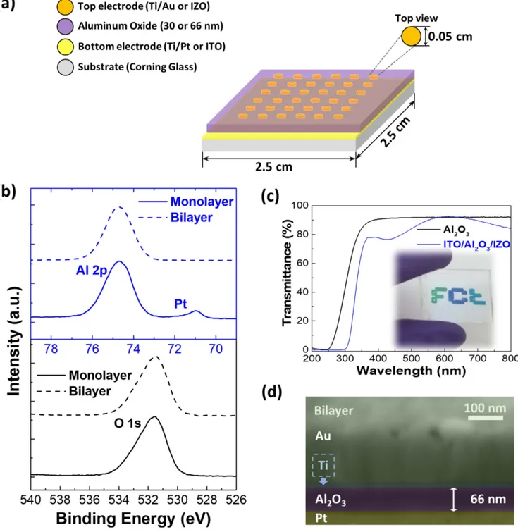
Figure 1(a) shows the schematic of the memories pro-duced with a monolayer or bilayer of aluminum oxide using metals (Ti/Au and Ti/Pt) and TCOs (ITO and IZO) as electrodes.
To further investigate the aluminum oxide and the effect of the subsequent depositions, XPS measurements were
performed. The Al 2p and O 1s emissions are shown in figure1(b). The Al 2p binding energy is found at 74.7 eV in the monolayer and the bilayer. Since this result is similar to values from literature in which charge referencing to C 1s was used, it can be concluded that our measurements did not suffer from artefacts due to charge accumulation [45].
A peak of metallic platinum(Pt 4f) at 71 eV is observed in the monolayer and not in the bilayer. This means that Pt intermixes with Al2O3 during the film formation in the first
layer. By using angle-resolved XPS it can be shown that with increased surface sensitivity the Pt signal disappears, there-fore the estimated depth from the surface up to which no platinum is present is approximately 5 nm (figure S2 in the supporting information). Besides the platinum signal in the monolayer sample, the surface contains oxygen and alumi-num as the main components, and a small percentage of carbon for all samples. Due to the convolution of the Pt 4f5/2 p and Al 2p peak, the Al 2s emission was used to calculate the O/Al ratio (spectra not shown here). After the first and sec-ond deposition, the O/Al ratio is approximately the same, 1.29 and 1.27, respectively.
In order to study the thinfilm’s transparency, the optical transmittance of the Al2O3 bilayer (66 nm) and the full
transparent memory (ITO/Al2O3/IZO) were measured,
showing 91% and 80% of transmittance respectively, as depicted infigure1(c).
The produced Al2O3thin films were also characterized
with ATR-FTIR before and after annealing at 500°C in order to monitor organic residues removal, as shown infigure S3 in the supporting information.
The structure of solution-based aluminum oxide thin films was investigated by XRD, as shown in figure S4 in the supporting information. The absence of diffraction peaks reveals that amorphous thin films are obtained for the alu-minum oxide even upon annealing at 500°C. Since the thin films are amorphous, they have no grain boundaries, low leakage current, and low surface roughness, thus improving device performance. High-resolution SEM-FIB cross-section images of the memories (Ti/Pt/Al2O3/Ti/Au) were
per-formed to measure the film’s thickness. The single-layer Al2O3thinfilm has a thickness of about 30 nm (figure S5 in
the supporting information) and the double-layer thin films have a thickness of about 66 nm, as depicted infigure1(d). Note that there is a considerable difference between the Al2O3
thickness from the SEM cross-section and the Pt found up to 5 nm below the surface. This is most likely due to the inter-mixing of the two materials at the interface and the limited resolution of the SEM.
The I–V curves of Ti/Pt/Al2O3/Ti/Au devices exhibit
unipolar resistive switching under a current compliance(CC) of 1 mA for the different thicknesses as depicted in figures 2(a), (d). For both conditions 36 devices were mea-sured. A low forming voltage at the negative side (∼−2 V) equivalent to the set voltage is required. These I–V char-acteristics were measured under consecutive DC voltage sweeps and the voltage was controlled through the Au top electrode.
In the case of the single-layer Al2O3, the memory showed
a stable and uniform switching behavior (figure 2(a)), how-ever after 19 cycles it was not possible to switch the memory on (figure 2(b)), showing low endurance. The device pre-sented a good retention of up to 105s in air, with an RON/OFF ratio of 105with a small degradation in the end. Figure2(c) shows the set and reset voltage, which had a small deviation of (−2.1±0.4) V and (−0.7±0.2) V respectively, that could be explained by the unpatterned Al2O3. Most of the
working devices were in the outer limits of the substrate, reducing the yield to 30%. The memories that were not
working, showed a short-circuit like behavior. This outcome is explained by the diffusion of Pt up to 5 nm below the Al2O3
thinfilm surface, which results in an ultrathin layer of intact Al2O3in the memory without any Pt diffusion. Note that both
XPS and SEM-FIB cross-sections where obtain from the center of the sample area.
Figure 2(d) shows the bilayer Al2O3 memory which
revealed better endurance when compared with the mono-layer, reaching 100 cycles (figure S6(a) in the supporting information). The resistance states uniformity measured in
Figure 1.(a) Schematic of memory structure; (b) XPS of Al 2p and O 1s emissions of solution-processed Al2O3films with one and two
layers;(c) optical transmittance of aluminum oxide bilayer on glass and of ITO/Al2O3/IZO; (d) high-resolution SEM-FIB cross-section
100 cycles is shown in figure S6(b) of the supporting information.
Taking that into account, retention tests were also per-formed at 85°C in vacuum to verify the reliability of the devices. For both temperatures a good retention of 105s with RON/OFF ratio of 105 was achieved, showing no significant degradation of HRS and LRS; this indicates that the device could maintain these properties for 10 years, as depicted in figure2(e). In terms of set and reset voltage, this device also showed a small deviation of(−2.2±0.6) V and (–0.6±0.1) V, respectively, as shown in figure2(f). The yield as com-pared to the monolayer memories was also improved, for the first time achieving 100% for these particular device types.
Note that an ultrathin layer of oxidized titanium at the interface of Al2O3and Ti contact is formed due to the
oxy-gen-getter property of titanium. This layer leads to a chemi-cally reactive contact which reduces the Al2O3and creates a
high concentration of oxygen vacancies at the Al2O3interface
with the top contact. This increases the local conductivity close to the top aluminum oxide interface[2]. This is in line with the I–V characteristics of the pristine state, which show a rectifying behavior(figure S7 in the supporting information). A higher electron barrier is observed at the Pt/Al2O3contact
compared to the Al2O3/Ti/Au contact. Thus, a preferential
negative electroforming at lower voltages can maintain the self-selecting resistive switching scheme.
A MLC operation can be obtained in the bilayer Al2O3
memories during the reset process. Figure 3(a) shows an example of I–V characteristics during the set and reset, and figure 3(b) the results of a retention test for distinct
two-resistance states at room temperature. This was performed in order to verify the reliability of the multi-level operation. To obtain MLC characteristics the reset process was adjusted in two different reset voltages. Once the device is programmed in one state, either level 1 (−0.5 V) or level 2 (−0.9 V), a good retention time of 104s is obtained. Higher voltage amplitudes accelerate local joule heating of the see[47] Thus, the MLC operation is due to a thermal-assisted electric field rupture model of the CF.
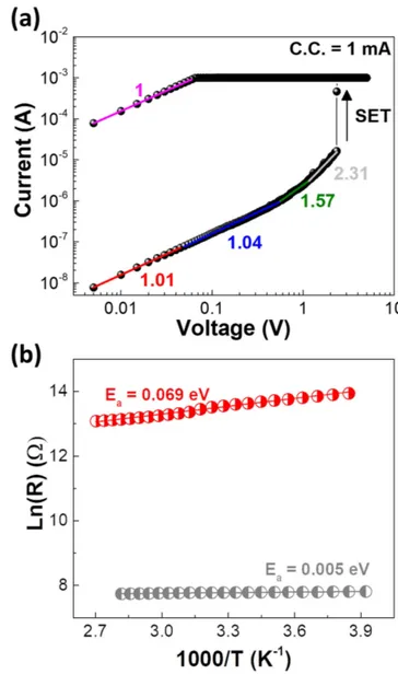
Thefitting of typical I–V characteristics in a log–log scale is shown infigure4(a). The space-charge-limited conduction (SCLC) mechanism following ohmic conduction in the low voltage region, square law (from 0.7 to 1.05 V) and steep increase region for voltages>1.1 V were observed at the off-state. The on-state shows ohmic behavior(slope of 1), indi-cating the presence of highly conductive paths. The results are in agreement with other reports on Al2O3 memories
[23,29,30].
At the low resistance state (on-state), temperature dependency is very weak with an activation energy (Ea) of
0.005 eV while the intermediate resistance state shows slight thermal activation (Ea=0.069 eV), as observed in
figure4(b). The trend of resistance versus temperature reveals a degenerated semiconducting-like phase as the nature of the CFs.
Based on the above presented results, the proposed mechanism of these unipolar or thermochemical resistive switching devices is the following: A filamentary thermal breakdown of the oxide increases the local doping between the top Ti contact (oxygen-poor region) and the bottom
Figure 2.Ti/Pt/Al2O3/Ti/Au electrical characterization of both memory conditions, monolayer (30 nm) and bilayer (66 nm): (a), (d) I–V
electrode (oxygen-rich region). The electroforming is an irreversible process, and the CFs are never completely rup-tured during set/reset operation. Thus, the set process always occurs at the lower voltages. In the reset process different stop voltages result in the partial thermal rupture (nano-scale antifuse process) of the CFs into variable sizes, which is then associated with the different resistance states. The interrelated effects of ohmic and SCLC conduction mechanism probably alter the activation energy of the intermediate state.
A fully transparent bilayer Al2O3ReRAM was produced
by replacing metallic electrodes with TCOs, ITO as bottom and IZO as top electrode. Figure5(a) represents the typical I– V curve of transparent unipolar memory writing and erasing. The set occurs when a negative bias voltage(0 to −6 V) is applied; an abrupt increase in the current was observed at −4.2 V, achieving the LRS. A compliance (CC) of 1 mA was established to prevent device breakdown. To reset the mem-ory a negative bias voltage(0 to −4.5 V) was applied without CC, and the memory reverted to the HRS at–4 V due to the
joule effect. Figure 5(b) shows the retention of the ITO/Al2O3/IZO memory. The device revealed a reliable
retention of up to 104s with a RON/OFFratio of 104without
deterioration. Table S1 in the supporting information depict other oxide transparent memories, and this is thefirst report of aluminum oxide obtained via a solution-based method for such devices.
Although their performance is not as good as that of non-transparent memories, these results clearly demonstrate the feasibility of a cost-effective System-On-Panel approach for transparent electronics.
4. Conclusions
In this work, we demonstrate for the first time the use of solution combustion synthesis (SCS) in the production of aluminum oxide memories. The physical properties of the
Figure 3.(a) Typical I–V memory characteristics showing set and the
reset with multi-level cell(MLC) operation; (b) multi-level retention characteristics for different reset voltages.
Figure 4.(a) I–V characteristics of Ti/Pt/Al2O3/Ti/Au device
plotted in log–log scale, showing a space-charge-limited conduction mechanism;(b) temperature analysis of the memory in different resistance states.
aluminum oxide layers were investigated using a wide range of characterization techniques that revealed high transparency (>90%) and the elimination of all residual organics. The Al2O3 memories were improved with by a dual stage
deposition process, which limits the Pt diffusion into the aluminum oxide. These ReRAM devices showed a unipolar resistive switching behavior with good endurance (100 cycles), retention time up to 105s at 85°C, and a yield of 100%. Also, a MLC operation was achieved by application of different reset voltages. Temperature analysis of various resistance states reveals a filamentary nature based on dif-ferent doping levels of the oxygen vacancies.
Furthermore, a fully transparent device using ITO/Al2O3/IZO showing good memory performance was
successfully produced, which paves the way for cost-effective System-On-Panel technology in transparent electronics.
Acknowledgments
This work is funded by FEDER funds through the COM-PETE 2020 Programme and National Funds through FCT-Portuguese Foundation for Science and Technology under project number POCI-01-0145-FEDER-007688, Reference UID/CTM/50025. European Community H2020 NMP-22-2015 project 1D-NEON Grant Agreement 685758. A Kia-zadeh acknowledges FCT-MCTES for a postdoctoral grant (Grant SFRH/BPD/99136/2013). E Carlos acknowledges FCT-MCTES for a doctoral grant (Grant SFRH/BD/ 116047/2016) and IDS-FunMat-INNO project FPA2016/ EIT/EIT RawMaterials Grant Agreement 15015. J Deuer-meier acknowledges funding received from the European Union through the project HERACLES (project number 700395). Authors would like to acknowledge J V Pinto and S Pereira for XRD, and D Nunes for SEM-FIB measurements.
Notes
The authors declare no competingfinancial interest.
ORCID iDs
Emanuel Carlos https://orcid.org/0000-0002-5956-5757 Asal Kiazadeh https://orcid.org/0000-0002-8422-5762 Rita Branquinho https://orcid.org/0000-0001-9771-8366 Rodrigo Martins https://orcid.org/0000-0003-3115-6588
References Q1
[1] Sawa A 2008 Resistive switching in transition metal oxides Mater. Today11 28–36
[2] Yang J J, Pickett M D, Li X, Ohlberg D A A, Stewart D R and Williams R S 2008 Memristive switching mechanism for metal/oxide/metal nanodevices Nat. Nanotechnol.3 429–33
[3] Vogel E 2007 Technology and metrology of new electronic materials and devices Nat. Nanotechnol.2 25–32 [4] Waser R, Dittmann R, Staikov C and Szot K 2009
Redox-based resistive switching memories nanoionic mechanisms, prospects, and challenges Adv. Mater.21 2632–63 [5] Waser R and Aono M 2007 Nanoionics-based resistive
switching memories Nat. Mater.6 833–40
[6] Yanagida T, Nagashima K, Oka K, Kanai M, Klamchuen A, Park B H and Kawai T 2013 Scaling effect on unipolar and bipolar resistive switching of metal oxides Sci. Rep.3 1–6 [7] Kim G H, Lee J H, Ahn Y, Jeon W, Song S J, Seok J Y,
Yoon J H, Yoon K J, Park T J and Hwang C S 2013 32×32 crossbar array resistive memory composed of a stacked schottky diode and unipolar resistive memory Adv. Funct. Mater.23 1440–9
[8] Qian K, Nguyen V C, Chen T and Lee P S 2016 Novel concepts in functional resistive switching memories J. Mater. Chem. C4 9637–45
[9] Chen Y S, Lee H Y, Chen P S, Wu T Y, Wang C C, Tzeng P J, Chen F, Tsai M J and Lien C 2010 An ultrathin forming-free HfOxresistance memory with excellent electrical
performance IEEE Electron Device Lett.31 1473–5
Figure 5.(a) Typical I–V characteristic and (b) retention of the
[10] Zhang Y, Wu H, Bai Y, Chen A, Yu Z, Zhang J and Qian H 2013 Study of conduction and switching mechanisms in Al/AlOx/WOx/W resistive switching memory for
multilevel applications Appl. Phys. Lett.102 1–5 [11] Kim S-T and Cho W-J 2018 Improvement of multi-level
resistive switching characteristics in solution-processed AlOx-based non-volatile resistive memory using microwave
irradiation Semicond. Sci. Technol.33 15009
[12] Chang M F et al 2012 Circuit design challenges and trends in read sensing schemes for resistive-type emerging nonvolatile memory ICSICT 2012—2012 IEEE 11th Int. Conf. on Solid-State Integrated Circuit Technology Proc. pp 2–5
[13] Kim K M, Choi B J, Koo B W, Choi S, Jeong D S and Hwang C S 2006 Resistive switching in Pt/Al2O3/TiO2/Ru
stacked structures Electrochem. Solid-State Lett.9 G343 [14] Lee M et al 2011 A fast, high-endurance and scalable
non-volatile memory device made from asymmetric
Ta2O5–x/TaO2–xbilayer structures Nat. Mater.10 625–30
[15] Choi B J et al 2005 Resistive switching mechanism of TiO2
thinfilms grown by atomic-layer deposition J. Appl. Phys. 98 33715
[16] Lee H Y, Chen P S, Wu T Y, Chen Y S, Wang C C, Tzeng P J, Lin C H, Chen F, Lien C H and Tsai M-J 2008 Low power and high speed bipolar switching with a thin reactive Ti buffer layer in robust HfO2based RRAM 2008 IEEE Int.
Electron Devices Meeting(Piscataway, NJ: IEEE) pp 1–4 [17] Baek I G et al Highly scalable
Q2 non-volatile resistive memory
using simple binary oxide driven by asymmetric unipolar voltage pulses IEDM Technical Digest. IEEE Int. Electron Devices Meeting 2004 pp 587–90
[18] Kim S and Choi Y K 2008 Resistive switching of aluminum oxide forflexible memory Appl. Phys. Lett.92 3–6 [19] Lee D, Choi H, Sim H, Choi D, Hwang H, Lee M-J,
Seo S-A and Yoo I K 2005 Resistance switching of the nonstoichiometric zirconium oxide for nonvolatile memory applications IEEE Electron Device Lett.26 719–21 [20] Kittl J A et al 2009 High-k dielectrics for future generation
memory devices(invited paper) Microelectron. Eng.86 1789–95
[21] Carlos E, Branquinho R, Kiazadeh A, Martins J, Barquinha P, Martins R and Fortunato E 2017 Boosting Electrical performance of high-κ nanomultilayer dielectrics and electronic devices by combining solution combustion synthesis and UV irradiation ACS Appl. Mater. Interfaces9 40428–37
[22] Kim S and Choi Y-K 2008 Resistive switching of aluminum oxide forflexible memory Appl. Phys. Lett.92 223508 [23] Baek I-J and Cho W-J 2017 Resistive switching characteristics
Q3
of solution-processed organic–inorganic blended films for flexible memory applications Solid. State. Electron. 0–1 [24] Wu Y W Y, Lee B L B and Wong H P 2010 Based RRAM
Using atomic layer deposition(ALD) with 1-RESET current IEEE Electron Device Lett.31 1449–51
[25] Yu S, Jeyasingh R, Wu Y and Philip Wong H S 2011 Understanding the conduction and switching mechanism of metal oxide RRAM through low frequency noise and AC conductance measurement and analysis Technical Digest-Int. Electron Devices Meeting IEDM pp 275–8
[26] Kim W, Park S I, Zhang Z, Yang-Liauw Y, Sekar D, Wong H-S P and Wong S S 2011 Forming-free nitrogen-doped AlOXRRAM with sub-μA programming current
2011 Symp. VLSI Technology-Digest Technical Paper vol 31, pp 22–3
[27] Prakash A, Maikap S, Banerjee W, Jana D and Lai C S 2013 Impact of electrically formed interfacial layer and improved memory characteristics of IrOx/high-κx/W structures
containing AlOx, GdOx, HfOx, and TaOxswitching materials
Nanoscale Res. Lett.8 1–12
[28] Chen Z, Zhang F, Chen B, Zheng Y, Gao B, Liu L, Liu X and Kang J 2015 High-performance HfOx/AlOy-based resistive
switching memory cross-point array fabricated by atomic layer deposition Nanoscale Res. Lett.10 70
[29] Park K and Lee J-S 2016 Reliable resistive switching memory based on oxygen-vacancy-controlled bilayer structures RSC Adv.6 21736–41
[30] Jang J, Song Y, Cho K, Kim Y, Lee W, Yoo D, Chung S and Lee T 2016 Non-volatile aluminum oxide resistive memory devices on a wrapping paper substrate Flexible Print. Electron.1 34001
[31] Yeom S-W, Ha H J, Park J, Shim J W and Ju B-K 2016 Transparent bipolar resistive switching memory on aflexible substrate with indium-zinc-oxide electrodes J. Korean Phys. Soc.69 1613–8
[32] Chen S, Lou Z, Chen D and Shen G 2018 An artificial flexible Q4
visual memory system based on an UV-motivated memristor Adv. Mater.1705400
[33] Trapatseli M, Cortese S, Serb A, Khiat A and Prodromakis T 2017 Impact of ultra-thin Al2O3–ylayers on TiO2–xReRAM
switching characteristics J. Appl. Phys.121 184505 [34] Yin Chen Y, Pourtois G, Adelmann C, Goux L, Govoreanu B,
Degreave R, Jurczak M, Kittl J A, Groeseneken G and Wouters D J 2012 Insights into Ni-filament formation in unipolar-switching Ni/HfO2/TiN resistive random access
memory device Appl. Phys. Lett.100 113513
[35] Jung K-H, Song S-G, Park K-W, Sok J-H, Kim K-M and Park Y-S 2017 Observation of AlOxmaterial in electrical
resistive switching for nonvolatile random access memory application J. Korean Phys. Soc.70 489–93
[36] Chang T-C, Chang K-C, Tsai T-M, Chu T-J and Sze S M 2016 Resistance random access memory Mater. Today19 254–64 [37] Sleiman A, Sayers P W and Mabrook M F 2013 Mechanism of
resistive switching in Cu/AlOx/W nonvolatile memory
structures J. Appl. Phys.113 Q5
[38] Nigo S, Kubota M, Harada Y, Hirayama T, Kato S,
Kitazawa H and Kido G 2012 Conduction band caused by oxygen vacancies in aluminum oxide for resistance random access memory J. Appl. Phys.112
[39] Gergel-Hackett N, Hamadani B, Dunlap B, Suehle J, Richter C, Hacker C and Gundlach D 2009 Aflexible solution-processed memristor IEEE Electron Device Lett.30 706–8
[40] Lorenz M et al 2016 The 2016 oxide electronic materials and oxide interfaces roadmap J. Phys. D: Appl. Phys.49 433001 [41] Rosa J, Kiazadeh A, Santos L, Deuermeier J, Martins R,
Gomes H L and Fortunato E 2017 Memristors using solution-based IGZO nanoparticles ACS Omega2 8366–72 [42] Sharma B and Rabinal M K 2016 A simple dip coat patterning of aluminum oxide to constitute a bistable memristor Mater. Res. Express3 126302
[43] Vescio G, Crespo-Yepes A, Alonso D, Claramunt S, Porti M, Rodriguez R, Cornet A, Cirera A, Nafria M and Aymerich X 2017 Inkjet printed HfO2-based ReRAMs:first
demonstration and performance characterization IEEE Electron Device Lett.38 457–60
[44] Kim M-G, Kanatzidis M G, Facchetti A and Marks T J 2011 Low-temperature fabrication of high-performance metal oxide thin-film electronics via combustion processing Nat. Mater.10 382–8
[45] Moulder J F, Stickle W F, Sobol P E and Bomben K D 1992 Handbook of X-ray Photoelectron Spectroscopy Q6
[46] Águas H, Mateus T, Vicente A, Gaspar D, Mendes M J, Schmidt W A, Pereira L, Fortunato E and Martins R 2015 Thinfilm silicon photovoltaic cells on paper for flexible indoor applications Adv. Funct. Mater.25 3592–8 [47] Sahu V K, Das A K, Ajimsha R S and Misra P 2018 Studies on
processes in TiO2thinfilm grown by atomic layer deposition