Fábio Daniel dos Santos Vidago
Licenciado emCiências da Engenharia Electrotécnica e de Computadores
A Downconversion Beamforming RF
Front-End in 130 nm CMOS technology
Dissertação para obtenção do Grau de Mestre em Engenharia Electrotécnica
Orientador:
Prof. Dr. João Pedro Abreu de Oliveira, Prof. Auxiliar,
Universidade Nova de Lisboa
Júri:
Presidente: Prof. Dr. Paulo Miguel de Araújo Borges Montezuma de Carvalho Arguente: Prof. Dr. Luís Augusto Bica Gomes de Oliveira
A Downconversion Beamforming RF Front-End in 130 nm CMOS technology
Copyright cFábio Daniel dos Santos Vidago, Faculdade de Ciências e Tecnologia, Uni-versidade Nova de Lisboa
A
CKNOWLEDGEMENTS
Gostaria de começar por agradecer à Faculdade de Ciências e Tecnologia da Universidade Nova de Lisboa, por estes 5.5 anos de aprendizagem, quer a nível académico, quer a nível pessoal. Estas competências adquiriras serão certamente de extrema importância para o meu futuro profissional.
Queria também agradecer ao Prof. João Pedro Oliveira, por ter aceite ser o meu orientador e me ter proporcionado um tema de tese extremamente interessante e muito atual, que me obrigou a trabalhar fora da minha área de conforto, quero também agradecer por todo o apoio e por tudo o que me ensinou, não só no âmbito da realização desta tese, mas também durante todo o curso. Ao longo deste curso, houve muitos professores, dentro e fora do departamento de Electrotecnia, que me marcaram, queria, portanto agradecer a todos eles, que me proporcionaram não só imensos conhecimentos mas também muitos bons momentos, dentro e fora das salas de aulas.
Quero agradecer aos meus colegas da sala 3.5, em nenhuma ordem em particular, Rúben Carvalho (que não pertence à sala), Ricardo Rodrigues, Filipe Rodrigues, Filipe Viegas, Carlos Oliveira e Élvio Mendes, pelos momentos de grande amizade. E aos meus colegas fora da 3.5, Ricardo Neto, Rui Calado, Rodrigo Jorge Francisco, José Ferreira, Rodrigo Fraústo, João Carvalho, Andreia Ribeiro e Sofia Rodrigues. Muito obrigado por todos os momentos e bons dias de trabalho.
Agradeço também aos meus grandes amigos, João Oliveira, Gomes, Gongas e Marques, por todos os bons tempos passados, e por todas a boas recordações. Um agradecimento especial à Filipa Cruz e à Marisa Castro, por todo o apoio.
A
BSTRACT
Due to the exponential growth of wireless data communications an increasing number of components compete for space in the frequency spectrum. Nowadays, different ap-proaches have been addressed in order to overcome this problem. One of these apap-proaches is using spatial filters instead of time-domain ones. Since most wireless devices operate by transferring/receiving signals to/from all directions, interfering signals are becoming an increasing problem. Thus steering the transmission/reception of signals in a specific direction alleviates this problem, which is performed by employing multiple antennas.
In the scope of the spatial filtering approach, a 1 GHz downconvertion 4-element phased array receiver front-end is presented in this thesis, implemented in 130 nm Com-plementary Metal Oxide Semiconductor (CMOS) technology. The phase shifting of the beamforming receiver is implemented with a switched-capacitor vector modulator, that excels in its linearity and low power consumption. This receiver also provides a spatial rejection of more than 20 dB and good input matching.
R
ESUMO
O crescimento exponencial das comunicações sem-fio levou a um decréscimo na disponi-bilidade do espectro de frequências. Hoje em dia várias abordagens diferentes têm sido alvo de grande atenção e desenvolvimento, com o intuito de resolver este problema. Uma dessas abordagens é, em vez de aplicar filtros temporais, aplicar filtros espaciais. Tendo em conta que os aparelhos sem-fio transmitem/recebem sinais para/de todas as direções, os sinais interferentes são cada vez mais problemáticos. Portanto, uma forma de resolver este problema é direcionando a recepção/emissão numa direção específica, para tal é necessário empregar várias antenas.
No âmbito da abordagem em filtros espaciais, um receptor de RF do tipo downconver-tionde 1 GHz com quatro antenas em fase é apresentado nesta tese, implementado em
tecnologiaCMOSde 130 nm. O desvio de fase para o construtor de feixe do receptor é
implementado com um circuito do modulador vectorial em condensadores-comutados, que proporciona um baixo valor de consumo de potência e alta linearidade. Este receptor proporciona uma rejeição espacial de mais de 20 dB e uma boa adaptação de impedância de entrada.
Palavras-chave: CMOS, SistemasMIMO, Construtor de feixe, Antenas em fase, Receptor
C
ONTENTS
Contents xiii
List of Figures xv
List of Tables xvii
1 Introduction 1
1.1 Motivation . . . 1
1.2 Thesis Outline . . . 4
2 Phased-Array Receiver Design 5 2.1 Beamforming . . . 5
2.1.1 Beam Steering . . . 6
2.1.2 Directivity . . . 9
2.1.3 Null Steering . . . 10
2.2 Basic Concepts . . . 11
2.2.1 Impedance Matching . . . 11
2.2.2 Scattering Parameters . . . 13
2.2.3 Noise . . . 15
2.2.4 Nonlinearities . . . 18
3 Beamforming RF Front-End Design 23 3.1 Common-Source Low-Noise Amplifier. . . 24
3.2 Mixer . . . 29
3.3 Trans-Impedance Amplifier . . . 34
3.4 Switched-Capacitor Vector Modulator . . . 37
3.5 GM-Stage. . . 42
3.6 Radio Frequency Filters . . . 43
4 Beamforming RF Front-End Simulation and Results 47 4.1 Low-Noise Amplifier . . . 47
4.2 Mixer . . . 51
4.3 Transimpedance Amplifier . . . 54
CONTENTS
4.5 Transconductance Stage . . . 59
4.6 Complete Beamforming Receiver . . . 62
5 Conclusion and Future Work 65
5.1 Conclusion . . . 65
5.2 Future Work . . . 66
L
IST OF
F
IGURES
1.1 a) Digital-MIMO beamforming receiver. b) Analog beamforming receiver. . . 2
1.2 Example of a radiation pattern. . . 3
2.1 Simplified block diagram of a beamformer. . . 6
2.2 Wave signal with a DOA ofθdegrees in a 4-element phased array receiver. . 7
2.3 Array factor plot of a 4-antenna phased array.. . . 8
2.4 Signal power and noise in a phased-array antenna.. . . 9
2.5 Array factors needed for null steering. . . 11
2.6 Example of incident and reflected waves in a generic circuit. . . 12
2.7 Plotted circles of constant values ofΓin theZLplane. . . 12
2.8 A two-port network. . . 13
2.9 Two-port networks where circuitsa,b,c, anddrepresent each scatter parameter. 14 2.10 Equivalent circuit of the thermal noise effect on a resistor. . . 16
2.11 Equivalent circuit of the thermal noise effect on a MOSFET transistor. . . 16
2.12 Illustration of noise in logarithmic scalevs. frequency. . . 17
2.13 Circuit equivelent of input referred noise in a circuit. . . 17
2.14 Illustration of the 1 dB compression point. . . 19
2.15 Illustration of the intermodulation phenomenon. . . 20
2.16 Illustration of the third order intercept point. . . 21
3.1 Architecture of the 4-element beamforming AFE. . . 23
3.2 Common-source LNA topology.. . . 25
3.3 LNA small signal model for input resistance computation. . . 26
3.4 LNA small signal model for NF calculation. . . 28
3.5 Graphic representation of the mixer operation. . . 30
3.6 Feedthrough representation in a mixer.. . . 30
3.7 Single-balanced mixer. . . 31
3.8 Double-balanced mixer. . . 32
3.9 Non-return-to-zero mixer. . . 33
3.10 Single-balanced non-return-to-zero mixer. . . 33
3.11 Transimpedance amplifier circuit.. . . 34
3.12 Operational amplifier circuit. . . 35
LIST OFFIGURES
3.14 Simplified schematic of the OpAmp. . . 36
3.15 Vector modulator principle. . . 38
3.16 Comparison between the sine and cosine functions and the approximated transfer function. . . 39
3.17 Sine an cosine approximation circuit. . . 40
3.18 Variable capacitor implementation. . . 41
3.19 Gm-stage circuit. . . 42
3.20 BPF frequency response. . . 44
3.21 LPF circuit. . . 44
3.22 LPF frequency response. . . 45
4.1 LNA circuit. . . 48
4.2 Plot of the input resistance of the LNA. . . 48
4.3 Plot of theS11of the LNA. . . 49
4.4 Plot of the gain of the LNA. . . 50
4.5 Plot of the noise figure of the LNA. . . 50
4.6 P1dBsimulation of the LNA. . . 51
4.7 Implemented mixer topology. . . 52
4.8 Voltage spectrum of the mixer input. . . 52
4.9 Voltage spectrum of the mixer output. . . 53
4.10 Noise figure plot of the mixer. . . 53
4.11 Implemented OpAmp circuit. . . 54
4.12 TIA time response. . . 55
4.13 TIA gain and phase.. . . 55
4.14 TIA noise figure.. . . 56
4.15 Switched-capacitor vector modulator. . . 57
4.16 Vector modulator sine approximation. . . 58
4.17 Vector modulator cosine approximation. . . 58
4.18 Vector modulator noise figure.. . . 59
4.19 Implemented transconductance stage. . . 60
4.20 Input and output voltages comparison in the gm stage. . . 60
4.21 Noise figure of the gm stage.. . . 61
4.22 Beamforming architecture. . . 62
4.23 Expected array factor with the beam steered to 0◦. (Adopted from [14]) . . . . 63
L
IST OF
T
ABLES
4.1 LNA transistor size parameters. . . 47
4.2 Mixer’s switches’ size parameters. . . 51
4.3 OpAmp transistor size parameters. . . 54
4.4 Phase shifter’s switches’ size parameters. . . 58
G
LOSSARY
I IP3 Input Third Order Intercept Point.
IP3 Third Order Intercept Point.
OIP3 Output Third Order Intercept Point.
P1dB 1 dB Compression Point.
ADC Analog-to-Digital Converter.
AF Array Factor.
AFE Analog Front-End.
BPF Band-Pass Filter.
CG Conversion Gain.
CMFB Common-Mode Feedback.
CMOS Complementary Metal Oxide Semiconductor.
DC Direct Current.
DOA Direction-Of-Arrival.
F Noise Factor.
GBW Gain-Bandwidth Product.
HPBW Half-Power Beamwidth.
IC Integrated Circuit.
IF Intermediate Frequency.
IM Intermodulation.
GLOSSARY
KVL Kirchhof Voltage Law.
LNA Low-Noise Amplifier.
LO Local Oscillator.
LPF Low-Pass Filter.
MIMO Multi-Input Multi-Output.
MOSFET Metal Oxide Semiconductor Field-Effect Transistor.
NF Noise Figure.
NMOS N-type Metal Oxide Semiconductor.
NRZ Non-Return-to-Zero.
OpAmp Operational Amplifier.
PMOS P-type Metal Oxide Semiconductor.
PSD Power Spectral Density.
RF Radio Frequency.
RZ Return-to-Zero.
SNR Signal-to-Noise Ratio.
TIA Trans-Impedance Amplifier.
C
H
A
P
T
E
R
1
I
NTRODUCTION
1.1
Motivation
The last decades have seen the rapid rise of wireless data communications. Throughout the years, in order to improve signal transmission, one of the approaches has been to increase signal bandwidth and/or spectral efficiency. But aggressive bandwidth increase leads to one problem, spectrum unavailability. In order to solve this problem Multi-Input Multi-Output (MIMO) systems were proposed. These systems promised to improve signal transmission and enhance data bit-rates, through the use of multiple antennas, in the transmission and/or emission ends [1,2]. However the support for this kind of system for the consumer electronics market has only recently started [3].
MIMO systems aren’t as recent as one might think. In the early 1940s some radar sys-tems, employing multiple antennas, were proposed to enhance reception, enable direction finding and increase jamming immunity. The technique that enabled the control of these MIMO systems was called beamforming. But only since 1990 have these systems become the target of heavy investigation. Nowadays MIMO systems have become an essential element of wireless communications standards, including Wi-Fi, 3G, 4G and in the future Massive MIMO has been regarded as a promising model for the high capacity demanded by 5G [4,5]. For improved link reliability some wireless communication standards have already adopted beamforming, for example the IEEE 802.15.3c Wireless Personal Area Network (WPAN), and since this protocol suffers from heavy signal path loss, over 16 antennas may be employed for multi-gigabit data rate [6].
CHAPTER 1. INTRODUCTION
antennas. Beamforming is a technique that can be employed to emit or receive a signal, its main goal is to achieve spatial selectivity to improve signal strength by rejecting interfering signals.
Figure1.1illustrates the block diagram of a typical digital-MIMO receiver and a analog beamforming receiver. In each design the Analog Front-End (AFE) amplifies and filters the incoming signal from each antenna, the signals then travel to each Analog-to-Digital Converter (ADC), where they’re converted into the digital domain, processed and the MIMO computation and decoding is performed. It’s rather obvious that each path in the MIMO system works much in the same way as a single-antenna system, up until the digital domain, thus the receiver is susceptible to interferers. These interferers may prove critical since it might put the ADC in a tight spot, and impose strict requirements upon its dynamic range. However, in the analog beamformer alternative, these interferers are ideally rejected, which in turn relaxes some the requirements of the ADC.
ADC Front End Digital Processing ADC Front End ADC Front End ADC Front End Digital Processing ADC Front End ADC Front End Analog Beamforming a) b)
Figure 1.1: a) Digital-MIMO beamforming receiver. b) Analog beamforming receiver.
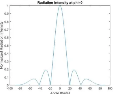
The term beamforming comes from the fact that spatial filters were designed to create beams in a desired direction. For example in figure1.2, the radiation pattern of the device is so that the emission of energy is maximized at a 0oangle, forming a beam of energy in that direction, thus “beamforming”.
Beamforming is especially useful when working with systems that receive spatially propagating signals, because if an interferer signal occupies the same frequency band as our desired signal, a temporal filter might not be enough to separate the signal from interference.
Spatial filtering might also be achieved by physically moving the antennas, but in some applications the antennas might be static and such a technique might not be effectively employed.
1.1. MOTIVATION
Figure 1.2: Example of a radiation pattern.
that the radiation pattern might be changed to achieve a better transmission or reception of the signal.
In an array of multiple antennas, if correctly designed, instead of receiving/emitting multiple independent signals, we can achieve a single narrower and more powerful signal beam pattern in one direction. In this case, beamforming can be achieved simply by employing a phase shift in the signal of each antenna to produce a beam in the desired direction, this array of antennas is called a Phased Array Antenna.
Besides the main lobe in the radiation pattern, side-lobes and nulls can also be con-trolled to ignore certain interferers in one particular direction while maintaining reception in others. This is also valid and useful on signal transmission.
Beamformers might be fixed or adaptive, the former uses fixed values for weightings and time-delays (or phasings), the latter adapts its values in real time, through the analysis of the signal received by the array, improving interference rejection. The adaptive process can be computationally intensive and some dedicated hardware processing might be required in order to effectively update the array’s weightings and phasings.
Beamforming has been the target of a lot of research each with different approaches, some based on injection locking [9], phase selection [10] and vector modulation. Within the vector modulation there are also some slight differences, such as cartesian combining [1,
CHAPTER 1. INTRODUCTION
1.2
Thesis Outline
This thesis is divided in five chapters, the introduction being the first one, the rest is organized as follows:
Chapter two covers all the basic concepts of beamforming as well as some Radio Frequency (RF) design parameters. In this part all the required concepts of phased antenna arrays are explained, these important topics will be used in order to design the receiver in the following chapters.
Chapter three presents all the necessary steps in order to design each block of the receiver as well as give an overview of the architecture . In this chapter all the equations used in the design of the receiver are presented and all the topologies used for each block introduced.
Next, in chapter four all the simulations necessary in order to analyse the receiver and each of its blocks are presented along with all the relevant results. Some of these simulations are: impedance matching, voltage gain, noise figure and compression point.
C
H
A
P
T
E
R
2
P
HASED
-A
RRAY
R
ECEIVER
D
ESIGN
It is crucial, in order to understand how a beamforming AFE receiver is implemented, to comprehend some analog phased-array antenna receiver fundamental properties. Thus, in this chapter some basic beamforming concepts will be briefly explained. This chapter also has the purpose of introducing some basic principles of RF electronic circuits. These basic concepts will be used in the explanation of the design of each block in the receiver, in chapter3.
2.1
Beamforming
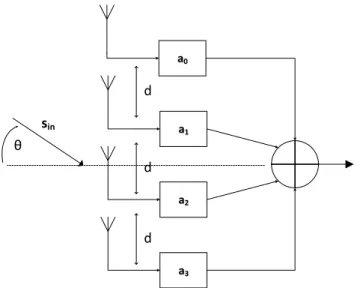
Let’s start by observing figure2.1, that depicts a simplified schematic of a beamformer. As we can observe there areNantennas and each has a weight ofaapplied to its signal, thus
the output at timetis given by the linear combination of theNantennas
sout(t) = N−1
∑
n=0an×sn(t). (2.1)
Since each antenna is equally spaced from each other, a distance ofdmeters, a signal
travelling with a Direction-Of-Arrival (DOA) ofθdegrees, figure2.2, will travel slightly different distances in order to meet each antenna in the array, lets call the difference in distance the length on then-th antennalngiven by
ln=n·dsin(θ), (2.2)
this difference in distance causes in each antenna a certain time delay proportional to the extra lengthln. Since the waves travel at the speed of lightc(≈3×10⁸m/s), the delay in
then-th antennaτnis
τn= ln
c =
n·dsin(θ)
CHAPTER 2. PHASED-ARRAY RECEIVER DESIGN
SUM
a1
s1(k)
a2
s2(k)
an
sn(k)
sout(k)
Figure 2.1: Simplified block diagram of a beamformer.
Supposing that a signal with amplitude Aand frequency f is sensed by the first antenna (n=0) its expression, in phasor form, is given by
s0(t) = Acos(2πf t) =Re{A.ej2πf t}, (2.4) thus the signal wave sensed by then-th antenna is
sn(t) = Acos[2πf(t+τn)] =Re{A.ej2πf(t+τn)}, (2.5)
sinceλ=c/f, combining equations2.3and2.5yields
sn(t) =Re{A·ej2πf t·ej2πn· d
λsin(θ)}, (2.6)
lastly combining2.6and2.1yields
sout(t) =Re
(
A·ej2πf t
N−1
∑
n=0an×ej2πn· d
λsin(θ)
)
. (2.7)
In conclusion the difference in the DOA of the signal wave, induces a different time of arrival between the antennas which in turn is transformed into an extra phase term.
2.1.1 Beam Steering
Now that we have the resulting signal of the beamformer from equation 2.7, we can proceed to the beam steering mathematics. In order to do so,anmust be quantized, first
this weight’s objective is to null the time delaysτn, due to the antenna spacing, thus we
have
an=e−j2π· d
2.1. BEAMFORMING
a0
a1
a2
a3
d
d
d
sin
θ
Figure 2.2: Wave signal with a DOA ofθdegrees in a 4-element phased array receiver.
where for simplicity’s sakeu0=sin(θ0), this substitution is called sine space or direction cosine space [p. 17][17]. After these weights are applied the signals in each antenna are aligned in time. In other words, the time delays generated through the element spacing, in each signal path are compensated in order to coherently combine the signals at the output [18]. After definingan, looking back at equation2.7, its value is maximized for a DOA
ofθ0. The effect of the weights summing is called Array Factor (AF) and it is basically responsible for the variable gain as a function of the DOA [p. 286][19]. The array factor is defined as
AF(u) = N−1
∑
n=0ej2πn·dλ(u−u0). (2.9)
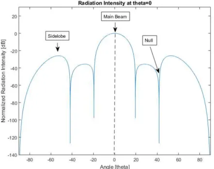
A typical response of the array factor as a function of the DOA is illustrated in figure
2.3. In this plot a larger lobe, the absolute maximum, can be found, its called the main beam, some lesser lobes can also be found, they’re defined as sidelobes. There are even some spots in the plot where the gain is zero, these are called the nulls. In essence, the array factor is the one responsible for the spatial filtering, the weights it adds in each path for each antenna govern the main beam, sidelobes and nulls, in order to direct the former to the wanted signal and the latter to the interferers.
When evaluating an AF one important parameter is the beamwidth, defined as the angular distance between two opposite points with the same maximum value. The Half-Power Beamwidth (HPBW) is the point at which the beam pattern assumes a value of half the maximum gain (≈-3 dB) [p. 42][19] . The equation that defines an HPBW is given by [p. 300][19]
u−3dB≈1.391 λ
CHAPTER 2. PHASED-ARRAY RECEIVER DESIGN
Figure 2.3: Array factor plot of a 4-antenna phased array.
Another important point about the array factor, is that the higher the ratio ofd/λis, the thinner the main beam becomes. If one wishes to design the narrowest main beam possible, the space between the antennas needs to be maximized. But there’s an important side-effect to take into account. Asd/λincreases, additional main beams may appear, these secondary main lobes positioned at directions other thanθ0, are defined as grating lobes. Thankfully, an equation exists to predict the appearance of these grating lobes, given by [20]
u=u0+i·λ
d , (2.11)
wherei ∈ Z, thus in order prevent the appearance of grating lobes a restriction to the maximum antenna spacing is imposed by
d
λmin ≤ 1
2. (2.12)
This restriction alters the definition of the array factor of2.9, sinceλminis the wavelength
for the maximum frequency of interest f0, thus AF is rewritten as
AF(u) = N−1
∑
n=0ejπn·
f
f0(u−u0). (2.13)
2.1. BEAMFORMING
2.1.2 Directivity
The directivityDof an antenna is an important metric to describe it. It is derived from the
beamwidth and, simply put, is the ratio between two signals of the same power, from an anisotropic antenna (a beam directed in a certain direction) for a certain DOA and an ideal isotropic antenna (the signal is radiated equally to all directions). It is defined as
Z π
−πD(θ)dθ=1 , (2.14)
for a scanning angle of[−180◦; +180◦].
It is obvious to conclude that since the AF governs the beamwidth and optimal DOA, it directly influences the directivity. Thus substitution in2.14yields
Z 1
−1|AF(u)|
2du=Z π
−πcos(θ)· |AF(θ)|
2dθ= N
∑
−1 n=0|an|2, (2.15)
Z π −π
"
cos(θ)· |AF(θ)|2/N
∑
−1 n=0|an|2
#
dθ =1 , (2.16)
where the first part of the integral "cos(θ)" is defined as the directivity of an element in the phased arrayDE, and the rest of the integral is defined asDA, the array directivity,
normalized by the summed power of the weights. Since the element directivity is, in essence, constant through all phased-array antennas, the array directivity is the most important value to report.
a0 a1 a2 a3 sin θ SIN NIN SIN NIN SIN NIN SIN NIN SOUT NOUT
Figure 2.4: Signal power and noise in a phased-array antenna.
Now thatDAhas been defined the next step is to take a look at the power that each
CHAPTER 2. PHASED-ARRAY RECEIVER DESIGN
after summing the resulting signal power is
Sout(θ) =Sin· |AF(θ)|2. (2.17)
After computing the power of the signal the next step is to quantize the noise output, that encapsulates the circuits’ input-referred noise as well as the noise due to signal propagation. The noise power is
Nout = Nin· N−1
∑
n=0|an|2. (2.18)
The ration between2.17and2.18is the Signal-to-Noise Ratio (SNR)1, which is equal to
Sout
Nout
(θ) = Sin
Nin ·
"
|AF(θ)|2/N
∑
−1n=0 |an|2
#
= Sin
Nin
·DA. (2.19)
Equation2.19yields an extremely important result, the array directivityDA, is directly
proportional to the SNR. Furthermore, theDAcan be interpreted as an improvement over
the SNR of a single element antenna [14]. This happens because since the noise present in each path can be considered uncorrelated to each other [21], thus if N antennas are used in the receiver the SNR can be improved by 10·log(N). In conclusion for each doubling in the number of antennas in the phased array, the SNR of the receiver improves 3 dB [1,
16,18].
2.1.3 Null Steering
In order to improve spatial selectivity there is a technique called Amplitude Tapering, that seeks to reduce the sidelobes’ amplitudes [22,23]. However there is a trade-off, because amplitude tapering reduces the array directivity, which means that the main beamwidth widens, this trade-off worsens as the number of antennas diminishes. Still, this technique can achieve a -10 dB drop in sidelobe amplitude below the main beam, in a phased-array with four antennas.
In any case, if the environment only has a single more powerful interferer signal, a null can be placed in its direction, achieving an effective rejection, this technique is called Null Steering [21]. As was mentioned in1.1, beamformers can be fixed or adaptive, and whether the direction of the interferer is known a-priori or calculated a-posteriori, is what defines them.
Looking at figure2.5, AFquies represents the array factor steered tou0, and uint the
direction of the interferer. The objective is to introduce a null in AFquies atuint without
disturbing the gain of the main beam steered towardsu0. Thus aAFintis created steered
towardsuint, with its main beam maximum scaled toAFquies(uint), thus when subtracting
2.2. BASIC CONCEPTS
u=sin(theta)
-1 -0.5 0 0.5 1
Array Factor [dB]
-100 -80 -60 -40 -20 0 20
AFint AFquies
u0
uint
Figure 2.5: Array factors needed for null steering.
the two array factors a null is introduced inuint. AFnull(u), the resulting array factor is
given by
AFnull(u) = AFquies(u)−AFint(u) = AFuni,u0(u)−AFuni,u0(uint)·
1
NAFuni,uint(u). (2.20)
This is only possible because the array factors have an important property, they’re linear. As in, a linear combination of array factors is equal to an array factor with the linear combination of the weightsan. For the resulting AF, its main beam remains unaltered and
atuinta null is present. Although if a sidelobe is present atAFint(u0), the pretended main beam will have a small gain loss of approximately 1 dB.
In conclusion, in order to improve spatial selectivity, for phased-array antennas with few elements it is preferable to use the null steering approach, however in receivers with more antennas, and many smaller interferers, amplitude tapering might be the most attractive technique.
2.2
Basic Concepts
2.2.1 Impedance Matching
When designing a Low-Noise Amplifier (LNA), there are many important parameters that need to be taken into account. One of these important parameters is impedance matching. Its importance stems from the fact that it is the process to reduce input return loss. When working with RF signals, sinceλ=c/f, the signal’s wavelength is such that, in practice
CHAPTER 2. PHASED-ARRAY RECEIVER DESIGN
will increase the power reflection. If a portion of the signal’s power is reflected back to the antenna, it means that less power is transferred to the receiver.
ZL Zs
Vs
i
r
Figure 2.6: Example of incident and reflected waves in a generic circuit.
Figure2.6shows the equivalent circuit to analyse this phenomenon. To better under-stand the relation between impedance matching and the reflection coefficientΓ, let us analyse the next equation:
Γ=
Zin−RS
Zin+RS
2
(2.21)
Since the impedance of an antenna is usually 50Ω (RS = 50 Ω), one can plot the
reflection coefficientΓin theZLplane, thus:
-20 dB
-15 dB -10 dB Im{Zin}
Re{zin} 50 Ω
Figure 2.7: Plotted circles of constant values ofΓin theZLplane.
In figure 2.7 each circle represents a constant value of Γ. Through figure 2.7 and equation2.21, one can observe that to minimize reflection and thus maximize the signal power transfer, one must simply design the input impedance of the LNA to be equal to the antenna output impedanceZS=ZL.
2.2. BASIC CONCEPTS
power is reflected, although one should strive to reduce this value further as to allow some safety margin. In conclusion designing LNAs requires circuit techniques that provide a 50Ωinput resistance and near zero input reactance, without the noise that a 50Ωresistor provides [p. 266][24].
2.2.2 Scattering Parameters
Scattering parameters or S-Parameters, are a mathematical aid to ease the measurement of power quantities when designing high-frequency circuits. There are two main reasons to preferring the use of power quantities over voltage or current ones. Firstly, measuring the average power is easier than measuring a voltage or current. Secondly, usually the traditional design is based around the power transfer between circuit stages. These S-parameters, that are a result of the power analysis of a circuit, are used to describe the stage.
To better understand S-parameters, let’s look at figure2.8. In this figure we can denote a generalization of a two-port network, where the incident and reflected waves at the input port,P1+andP1−, respectively, are present. Similarly,P2+andP2−represent the incident and
reflected waves at the output port, respectively [p. 72][24].
Two-Port
Network
Rs RL Vin P1+ P1- P2-P2+Figure 2.8: A two-port network .
These four quantities, above described are related to one another through the S-parameters of the network, where:
P1−= S11P1++S12P2+ (2.22)
P2−= S21P1++S22P2+ (2.23)
Another representation for this relation is through a scattering matrix:
"
P1− P2−
#
=
"
S11 S12
S21 S22
#
×
"
P1+ P2+
#
(2.24)
CHAPTER 2. PHASED-ARRAY RECEIVER DESIGN Two-Port Network Rs RL Vin P1+
P1-P2+ = 0
Two-Port Network Rs RL Vin P1+ P1-Two-Port Network Rs P2-P2+
P2+ = 0 Vx Rx
P1+ = 0
Two-Port Network Rs P2-P2+ Vx Rx
P1+ = 0 (c)
(a) (b)
(d)
P2-
P1-Figure 2.9: Two-port networks where circuitsa,b,c, anddrepresent each scatter parameter.
As we can observe from figure2.9S11is related with the reflected and incident waves at the input port, meaning the input reflection coefficient, which represents input matching accuracy
S11 = P
−
1
P1+|P2+=0. (2.25)
S12is related with the reflected wave at the input port and the incident wave of the output port. This parameter can be interpreted as the “reverse isolation” of the system, meaning how much of the output signal travels backwards to the input source
S12 = P
−
1
P2+|P1+=0. (2.26) Similarly toS11,S22is the related with the incident and reflected waves at the output port, thus it also represents a reflection coefficient but this time for output matching
S22 = P
−
2
P2+|P1+=0. (2.27) Lastly,S21is related with the incident wave on the load and the incident wave of the input. Thus this parameter represents the power gain of the circuit
S21 = P
−
2
P1+|P2+=0. (2.28) Since modern RF design doesn’t strive for between-stage matching,S11andS21are the most important parameters. As most circuits include reactive and/or active components one can easily conclude that s-parameters aren’t scalar quantities, but often frequency dependent values (dependent of jω). It is important to point out that henceforth, s-parameters will be expressed in dB
2.2. BASIC CONCEPTS
2.2.3 Noise
Noise is random, this means that the instantaneous value of noise cannot be predicted. It’s an extremely important phenomenon to study when designing a RF system, since in an ideal world without noise or distortion, communication would be possible over any distance. In this chapter some basic notions about noise will be briefly explained.
As previously mentioned noise is random so, one might wonder how to properly study this phenomenon. The answer is simple because noise components in electrical circuits have a constant value of average power [p. 37][24], thus it can be defined as follows:
Pn= lim T→∞
1
T
Z T
0 x
2(t)dt. (2.30)
One might reach the conclusion that studying noise in the time-domain is ineffective, however in the frequency domain, more useful and insightful information can be extracted. If the values for all frequency components of a noise signal are measured, the result is called the Power Spectral Density (PSD). The resulting plot of the PSD is the average power of the noise signal over the frequency.
In the next two sections, two main noise sources will be explained, since they’re the most important and the ones primarily taken into account throughout the circuit’s design. These two sources are: thermal and flicker noise.
Thermal Noise
This phenomenon occurs because the ambient temperature, creates random agitations in the charge carriers and thus, noise. In a resistor this noise value can be modelled by a Thevenin equivalent circuit with a voltage source ofVn2 =4kTR1, or the Norton equivalent with a parallel current source of In2 = 4kT/R1, figure 2.10. Where k is the Boltzmann
constant,Tthe temperature measured inKelvinandR1is the resistance of the component, in this example a resistor. The last sentence leads to an interesting conclusion: the device doesn’t need to contain an explicit resistor to exhibit thermal noise.
In a Metal Oxide Semiconductor Field-Effect Transistor (MOSFET) transistor, operating in the saturation region, the thermal noise can be roughly described as a current source between the source and drain terminals, alternatively it can be approximated by a voltage source in series with the transistor’s gate, as shown in figure2.11.
The value of the noise equivalent current source is:
In2=4kTγgm, (2.31)
and the equivalent voltage source is:
Vn2=4kTγ/gm. (2.32)
Wheregmis the transistor’s transconductance, andγis the excess noise coefficient. Its value
CHAPTER 2. PHASED-ARRAY RECEIVER DESIGN
4kTR1 R1
R1 4kT/R1
Figure 2.10: Equivalent circuit of the thermal noise effect on a resistor.
4kT
γ
/gm
4kT
γ
gm
Figure 2.11: Equivalent circuit of the thermal noise effect on a MOSFET transistor.
γis usually obtained by measurements. The gate resistance is another noise source, but its value is many times smaller than the “drain-source” current source equivalent, so it is omitted [p. 43][24].
Flicker Noise
Flicker noise is another type of noise that MOSFET transistors suffer from, it is modelled by a voltage source in series with the transistor’s gate2, and its PSD is given by:
Vn2=
K W LCox
1
f . (2.33)
In the previous equationKis a process dependent constant, usually lower for P-type Metal
Oxide Semiconductor (PMOS) than N-type Metal Oxide Semiconductor (NMOS),Coxis
the gate oxide capacitance,W is the channel bandwidth,Lits length and f the frequency.
As we can observe there is a 1/frelation, because of this flicker noise is sometimes referred
to as "1/f noise".
2Much like thermal noise, flicker noise can also be modelled by a current source between the drain and
2.2. BASIC CONCEPTS
An interesting observation is that, when plotted, flicker and thermal noise intercept at a certain point of frequency, called the corner frequency, fc. Figure2.12illustrates this
effect:
f
f
cN
oi
se
(
dB
) Flicker Noise
Thermal Noise 1/f Corner
Figure 2.12: Illustration of noise in logarithmic scalevs. frequency.
Since the circuit presented in this dissertation is an RF designed circuit, one might wonder the relevance of flicker noise at higher frequencies due to its 1/f relation. This
effect isn’t negligible, since in can reach the RF range.
Noise Measurements
Above some of the basic concepts of how to modulate noise in a circuit were explained. Based on those explanations, this section will briefly introduce how noise is measured in a circuit.
The first step is to refer the noise of the circuit to the input. This is done because analysing the noise values at the output can be inconclusive, since an output with a high noise value might occur because of the high gain of the circuit and not necessarily a high noise. Figure2.13shows how this is modelled.
Noisy Circuit Model A
Noiseless Circuit Model B V2n
I2n
Figure 2.13: Circuit equivelent of input referred noise in a circuit.
CHAPTER 2. PHASED-ARRAY RECEIVER DESIGN
gain. Since at high frequencies these input-referred sources prove difficult to compute, a concept was introduced that allows an easier measurement of the noise performance in a circuit. This metric is called the Noise Figure (NF), or Noise Factor (F)3.
In circuit design one might, instead of trying to measure the noise level itself, measure the SNR. SNR is the signal power divided by the noise power. If the input and output SNR are the same, it means the circuit is noiseless, but to quantify how noisy it is, noise factor is expressed as
NF = SNRi
SNRo . (2.34)
In a noiseless circuit the previous equation is equal to one. NF is the F expressed in decibels, since each SNR is a dimension of power, it is defined as:
NF|dB=10logSNRi
SNRo
. (2.35)
A receiver usually has a chain with many stages, so it is important to compute the NF of the overall cascade, in terms of each stage. For example in a two stage cascade the total noise figure is given by
NFtot = NF1+ NF2−1
AP1
. (2.36)
One thing that is important to note is that the NF of the second stage has in its denominator the available power gain of the first stage, AP1, but the NF of the first stage has no dependencies of the following stage. Generalizing formstages we have
NFtot =1+ (NF1−1) + NF2−1
AP1 +...+
NFm−1
AP1×...×AP(m−1)
. (2.37)
The previous expression is called Friis’ equation [25]. An important conclusion is, that the noise contribution of each stage decreases as the total gain of the preceding stage cascade increases. However if a stage suffers from attenuation the noise figure contribution of the succeeding stages rises. This also means that the first stage of the receiver, usually the LNA, is the most important, noise-wise, since it has no dependencies besides itself, and its gain directly influences the total noise of the cascaded stages.
2.2.4 Nonlinearities
When a RF circuit is designed it is usually based around linear models for small signal operations, but some nonlinearities can occur and lead to some interesting phenomena not anticipated by the linear models, for example we assume that most amplifiers have a fixed gain for a certain frequency range, however this isn’t always so. In this section some nonlinearities will be briefly explained, these metrics will be used at a later part of this work to evaluate the linearity of some blocks.
2.2. BASIC CONCEPTS
Gain Compression
One of the nonlinearities is the assumption that the small signal gain of a circuit is independent of the present harmonics. But this is not the case when working with non-ideal components. If the amplitude of a harmonic is high enough, it can lead to compressive behaviour in the amplifier, meaning that as the input amplitude rises the gain decreases. This effect is quantified by the 1 dB Compression Point (P1dB), it is defined as the point
at which the input signal causes the gain to drop by 1 dB. The value for the compression point isn’t chosen arbitrarily, because a 1 dB compression point represents a 10% reduction in the gain, and it is a very important metric to characterize RF circuits and systems [p. 18][24].
Compression can be expressed in terms of voltage or power quantities although from this point onward whenever compression is discussed it will always be in terms of power quantities.
In figure2.14we plot the input powervsthe output power, and its result as we can
observe, is a line and its slope is the gain. As the input power continues to rise, upon reaching a certain value the gain begins to decrease, as explained above the amplifier goes into compression, and at the point at which the power drops 1 dB below the expected value we can find the circuit’s 1 dB compression point.
P o w er o u tp u t (d B m )
Power input (dBm)
P1dB Compression Region Response Asymptote Actual Response 1 dB
Figure 2.14: Illustration of the 1 dB compression point.
CHAPTER 2. PHASED-ARRAY RECEIVER DESIGN
Thus, if the compression point is known we can restrict the input levels to prevent the saturation of the amplifier and its non-linear consequences.
It is also important to note that 1 dB compression point can also be specified in terms of the output level at which it occurs, analysing the compression point in terms of input or output power depends on the application either in the transmission or receiving path.
This characteristic is measured by driving a sine wave at the input of the amplifier for a certain frequency and plotting its response, meaning the output power, thus creating the graphic of the figure2.14.
In conclusion, the higher theP1dB, the more linear and robust an amplifier is.
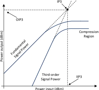
Intermodulation Products
In this section another important consequence of a circuit’s nonlinearity will be briefly explained. When two signals are applied to a nonlinear system, its output can exhibit com-ponents that result from the mixing of its inputs, this is called intermodulation product.
To better understand the effects of intermodulation let us take for example two signals with frequencies ofω1andω2. When applied to a nonlinear system these frequencies are multiplied and new signals are produced with a frequency ofω1−ω2andω1+ω2, that can be easily filtered. However, higher order mixing can occur which produces potentially interfering signals close to our work frequency that may not be easily filtered. Usually the most worrisome are the third-order IM products, 2ω1±ω2and 2ω2±ω1, of which the most possible to occur within the system’s frequency range are 2ω1−ω2and 2ω2−ω14. Figure2.15illustrates this phenomenon:
Nonlinear System
ω1 ω2 ω1 ω2
2 ω 1 -ω 2 2 ω 2 -ω 1 ω 1 -ω 2 ω 1 + ω 2 2 ω 1 + ω 2 2 ω 2 + ω 1
Figure 2.15: Illustration of the intermodulation phenomenon.
As we can observe ifω1is close toω2, the third order products 2ω1−ω2and 2ω2−ω1 will also be close to our signal making it extremely hard or even impossible to filter.
Now that we have acknowledged the importance of intermodulation products, the next step is to find a method to measure them. This metric exists and it is called the Third Order Intercept Point (IP3). The concept of theIP3originates from the fact that if the power or amplitude of the input signal rises, its intermodulation products rise more sharply, thus the IM products eventually become equal to that of our signal of interest. On a logarithmic scale, the third order products increase at a rate three times higher than that of first-order products (the input signals), because of the mathematics of mixing [pg. 21][24].
4Higher order products also exist but usually they lie far away in terms of frequency, thus heavily filtered
2.2. BASIC CONCEPTS
Similarly to the P1dB explained in the previous section, plotting the output power
versus the input power of our fundamental signal power and also the third-order signal power, we can find the point where these intersect and it’s called theIP3, figure2.16is an example of anIP3plot.
P
o
w
e
r
o
u
tp
u
t
(d
B
m
)
Power input (dBm)
Compression Region IP3
OIP3
IIP3 Third-order
Signal Power
Figure 2.16: Illustration of the third order intercept point.
The value of IP3 can be read with reference to the input or output powers, called Input Third Order Intercept Point (I IP3) or Output Third Order Intercept Point (OIP3), respectively. From this point onward in this thesis IP3 will be written rather thanI IP3, since the input will be the reference of interest.
C
H
A
P
T
E
R
3
B
EAMFORMING
RF F
RONT
-E
ND
D
ESIGN
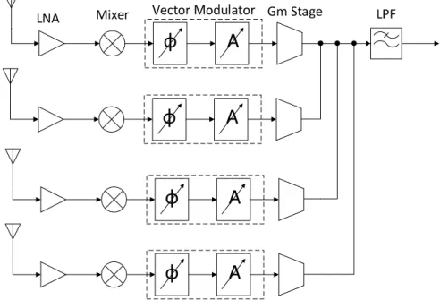
In the previous chapter the basic concepts required to design the AFE were introduced. In this chapter the necessary steps for the design of each block in the receiver will be explained. Figure3.1, schematically depicts the architecture intended for the beamforming RF front-end.
Mixer LNA
φ
A
Vector Modulator Gm Stage LPF
φ
A
φ
A
φ
A
Figure 3.1: Architecture of the 4-element beamforming AFE.
CHAPTER 3. BEAMFORMING RF FRONT-END DESIGN
signal. Then a passive single-balanced mixer with four paths, controlled by 4 out-of-phase 25% duty-cycle LOs, generate four different signals, in-phase (I+), quadrature (Q+, 90◦),
opposed-phase (I-, 180◦) and quadrature opposed-phase (Q-, 270◦). The following block,
the TIA converts the current signals from the mixers to voltage signals that are fed into the switched-capacitor vector modulator, that performs the phase-shifting. Next the Gm-stage, converts the signals into the current domain in order to sum the signals from the four elements, finally the signal are converted back into the voltage domain through load resistors and filtered with a Low-Pass Filter (LPF) to remove the higher frequency harmonics.
Since this architecture didn’t yield the pretended results, a second more simple one was implemented, the second one is very similar to the first, and it works as follows: the LNA performs a voltage amplification, the double-balanced mixer operates in the voltage domain, providing the same outputs (I+, I-, Q+ and Q-), a simple ideal voltage buffer separates the mixer and the phase shifter, and as with the first architecture the same gm stage performs element summing in the current domain, the resistors convert the signals back into the voltage domain and a LPF filters the unwanted higher frequencies.
3.1
Common-Source Low-Noise Amplifier
The Low-Noise Amplifier is usually the first stage of a receiver, thus its role is a critical one for the overall performance. As seen in section2.2.3, through the Friis’ equation2.37, to minimize the overall NF of the receiver the LNA must be designed to have a high gain and low NF, since it directly affects the succeeding stages’ noise performance. In a typical RF receiver a total noise figure of 6 to 8 dB is to be expected, for which the LNA’s contribution is of about 2 to 3 dB [p. 255][24], leaving the rest to the subsequent blocks.
One might deduce that the gain should be as high as possible to minimize the NF of the receiver. But this leads to a decrease in linearity, so a compromise must be made between minimizing the noise contribution of the subsequent stages and the linearity of the receiver.
Another important aspect to take into account is the power transfer from the antenna to the next stages, thus, as explained in the section2.2.1, a good input matching must be achieved. In essence, the input resistance of the LNA must be 50Ωand the reactance must be close to zero.
3.1. COMMON-SOURCE LOW-NOISE AMPLIFIER
VDD
Ls M1 M2 M3
Lg Rs
Vin
Vb1 Vb2
Vout RP
RN
Figure 3.2: Common-source LNA topology.
Gain
The first step in the LNA design was to compute its gain, as such the DC gain of this LNA topology is given by
Av= Vout
Vin
= gm1×Rout, (3.1)
wheregm1is the transconductance of the transistorM1andRoutis the output resistance.
The resistanceRoutis the parallel of two resistances,RPandRN, the impedances of the
PMOS transistorM3and the cascode impedance of transistorsM1andM2, respectively. Thus
Rout=RP kRN, (3.2)
whereRP =rds3and
RN =rds1· gm2
gds2, (3.3)
CHAPTER 3. BEAMFORMING RF FRONT-END DESIGN
Biasing
It’s been established that the LNA’s transistors need a high transconductance in order to achieve a high gain, which means that the transistors need a reasonable value for its drain-source current, Ids. TheM1andM3are each biased with a 1 : 1 ratio current-mirror.
These two transistors impose the necessary current in the LNA, so the biasing of M2is done by simply connecting its gate toVDD.
Impedance Matching
As it can be seen in figure3.2, the circuit uses reactive components, in this case two inductors, to perform impedance matching. In order to compute the input impedance of the LNA, the small signal model must be drawn and analysed. Figure3.3illustrates this very model, where the transistor’s gate-drain and source-bulk parasitic capacitances,Cgd
andCsb, respectively , were neglected.
Lg
Cgs
Vin
Rds
Ls
G
D
S
KVL
Figure 3.3: LNA small signal model for input resistance computation.
To find the expression of the input impedance of the LNAZin, the Kirchhof Voltage
Law (KVL) was applied, yielding:
Vx =VLg +VCgs+VLs
Vx = Ix·jωLg+Vgs+ (Ix+gmVgs)·jωLs
Vgs = Ix·
−j 1
ωCgs
Vx = Ix·jωLg+Ix·
−j 1
ωCgs
+Ix·jωLs+gm·Ix·
−j 1
ωCgs
·jωLs
Zin = Vx
Ix
= jωLg+
−j 1
ωCgs
+jωLs+gm· Ls
Cgs
Zin = gmLs
Cgs +j
ω(Lg+Ls)−
1 ωCgs
3.1. COMMON-SOURCE LOW-NOISE AMPLIFIER
After deducing the expression forZin, the next step is to equate the real and imaginary
parts, to 50Ωand 0Ω, respectively.
gmLs
Cgs
=50Ω⇔Ls =
50·Cgs
gm . (3.5)
The previous equation is used in order to fix the value forLs, now in order to null the
imaginary part ofZin
ω(Lg+Ls)− 1 ωCgs
=0⇔ Lg = 1 ω2·Cgs
−Ls. (3.6)
A quick look at equation3.5leads to an interesting conclusion, since a transistor’s
Cgsis usually very small, sometimes a few fF of capacitance only, and thegmis usually
lower then a couple dozen mS, this means thatLsmust have an extremely low inductance,
probably below 100 pH. Also in RF Integrated Circuit (IC) design a bond wire is inevitable in packaging, and it must be taken into account. This bond wire usually has an inductance no lower than a couple hundread pH to a few nH. These facts in conjunction lead to a paradox, on one hand we need a rather low value of inductance to achieve input matching, on the other hand, we already have an inductance of a couple nH present. An important question arises, how can a 50Ωresistance be obtained?
Looking back at the real part of equation3.5, one might reducegm or increase Cgs
accordingly, to try to raiseLs. The easiest method is usually to place a capacitor of a few
pF between the source and gate of the transistor in order to artificially increaseCgs, which
means thatLscan assume higher values. In this case the bond wire’s inductance serves as
the inductorLs.
The Lg inductor is off-chip so there are fewer restrictions for its inductance value,
achieving higher values ofQwhich is the inductor’s quality factor given by
Q= ωL
Rs
, (3.7)
whereωis the operating frequency,Lthe inductance value andRsthe equivalent series
resistance of the inductor’s windings.
Noise
Lastly, to find this topologies’ NF let’s start by looking at figure3.4. The current sourceIn1 represents the noise source of the transistorM1, andIoutthe output of the LNA1, thus
Iout=gmVgs+In1⇔Vgs = Iout−In1
gm . (3.8)
Similarly to the input impedance calculation steps for equation3.4, the KVL yields
Vin =s(Rs+sLg)VgsCgs+Vgs+sLs(Iout+sVgsCgs), (3.9) 1R
sis the resistance of the voltage source, meaning, the antenna resistance usually 50ΩbutLsis the
CHAPTER 3. BEAMFORMING RF FRONT-END DESIGN
Lg
Cgs
Vin
Ls
G
D
S
KVL
In1
Iout
Rs
Figure 3.4: LNA small signal model for NF calculation.
since substitution ofVgsfrom3.8, yields
Vin = sLsIout+s2(Ls+Lg)Cgs+1+sRsCgs· Iout−In1
gm , (3.10)
as it was previously mentioned when discussing input matching,LsandLgwere designed
to resonate withCgsatω0, meaning that(Ls+Lg)·Cgs= ω20, thus ifs = jω0
s2(Ls+Lg)·Cgs+1=0 , (3.11)
and the substitution of3.11into3.10gives
Vin = Iout·
jω0Ls+
jω0RsCgs
gm
−In1jω0RsCgs
gm . (3.12)
In the last equation the coefficient of Iout represents the transconductance gain of the
circuit, given by
Iout Vin = 1 ω0
Ls+ RsgmCgs
. (3.13)
As previously stated the circuit’s been input matched and one of the conditions for input matching was thatgmLs/Cgs = Rs, and also sincegm/Cgs ≈ ωTis the maximum
switching frequency of the transistor, its substituion in3.13gives
Iout Vin = ωT
2ω0· 1
Rs
. (3.14)
This last equation raises an important conclusion, when input matched, the transconduc-tance gain of the circuit is independent ofLs, Lgand gm. The next step is to nullVin, so
from equation3.13we have the output noise from transistorM1
|In,out|=|In1| ·
RsCgs
gmL1+RsCgs
3.2. MIXER
and much like it was done for the transconductance gain of the circuit, sincegmLs/Cgs=
Rs, the previous equation yields:
|In,out|= |In21|, (3.16)
from2.31in section2.2.3, we have
In2=4kTγgm. (3.17)
Thus, dividing the output noise current by the transconductance gain of the circuit and by 4kTRswhile adding 1 to the final result, the expression for the LNA’s noise is given by
equation3.18[p. 289] [24]
F=1+gmRinγ
gmω0
Cgs
2
. (3.18)
This last expression, which as previously stated only holds true if the circuit is impedance matched at the resonating frequency, shows that this topology can provide low noise values [p. 289][24].
3.2
Mixer
The mixer is a very important stage in receiver or transmitter architectures, because it performs a frequency translation by multiplying two waveforms, as shown in figure3.5. There are two kinds of mixers, upconversion and downconversion, used in the transmit and receive paths, respectively. In this dissertation a downconversion mixer was designed to convert a RF signal into an Intermediate Frequency (IF) signal. There are also two other main categories for classifying mixers, passive and active, the former uses transistors operating as switches, the latter uses transistors that operate as amplifiers. Since passive mixers have low power consumption a passive topology was chosen, explained below.
The mixer has three ports, two inputs and an output. In the downconversion case, the former are the RF and Local Oscillator (LO) ports, and the latter is the IF port. As illustrated in figure3.5, for example, if the LO signal isVLO(t) =cos(2πfLOt), and the RF
isVRF(t) =cos(2πfRFt), the IF signal will be given by
VIF(t) = K2[cos(2π(fRF− fLO)t) +cos(2π(fRF+ fLO)t)], (3.19)
whereKis the mixer’s conversion loss. The desired frequency component of equation3.19
is the IF one (fIF = fRF− fLO), this component can be isolated through the use of a LPF.
CHAPTER 3. BEAMFORMING RF FRONT-END DESIGN
Local Oscilator
(fLO) Radio
Frequency (fRF)
Intermediate Frequency
(fIF) RF LO IF Frequency Downconversion P o w e r Local Oscilator
(fLO) Radio
Frequency (fRF)
Intermediate Frequency
(fIF) RF LO IF Frequency Upconversion P o w e r
Figure 3.5: Graphic representation of the mixer operation.
As with the noise, theIP3of the mixer is also divided by the LNA’s gain. This leads to a compromise between noise and linearity, a consequence of this is that the design of the mixer and the LNA are linked. It’s common to, while designing the mixer, return to the LNA’s design in order to achieve a higher gain to compensate a poor noise or linearity performance by the mixer.
Clock Feedthrough
When designing a mixer, especially if realized by a MOSFET, unwanted coupling between the inputs and outputs of the device may occur, because the transistors have parasitic capacitors. What this means is that if the capacitances are large enough, the LO signal might, for example travel to the RF and/or IF ports. This effect is called port-to-port feedthrough, graphically represented in figure3.6. The LO to RF feedthrough is prejudicial since it produces offsets in the IF port and LO signals back to the antenna, on the other hand the LO to IF feedthrough can usually be suppressed through a LPF [24].
RF LO IF RF LO IF RL
Figure 3.6: Feedthrough representation in a mixer.
3.2. MIXER
3.20which characterizes the MOSFET capacitances in the saturation region [p. 124][26]
Cgs =Cgd =W·L·Cox′ , (3.20)
whereW andLare the transistor’s channel width and length, respectively andCox′ is the
device capacitance per unit of area. So in order to reduce port-to-port feedthrough, one must simply take special care with the device size.
Looking back at the circuit in figure 3.6, it’s easy to denote that this simple mixer topology, since it operates with single-ended RF and LO inputs, discards the RF signal every half of a LO period. In order to eliminate this efficiency deficit, another mixer can be added to the RF port, with a differential LO input, this topology illustrated in figure3.7is called a passive single-balanced mixer [p. 355][24].
V
RFV
LO+V
out+RL
V
LO-V
out-RL
Figure 3.7: Single-balanced mixer.
Besides doubling the conversion gain (or increasing by 6 dB), the single-balanced mixer also provides differential IF outputs with a single-ended RF input.
Another more advanced topology where two single-balanced mixers are employed to reduce and sometimes eliminate LO-IF feedthrough also exists and it’s called a double-balanced mixer, the circuit is illustrated in figure3.8. Mixers, broadly speaking, can also be separated into two categories, passive and active. Each of these categories can be implemented as single-balanced or double-balanced. The main difference is that passive mixers don’t employ transistors that operate as amplifiers, while the active counterparts do. In this thesis a passive mixer topology was chosen, for its lower power consumption, leaving the other blocks in the AFE to accommodate the receiver gain.
Conversion Gain
CHAPTER 3. BEAMFORMING RF FRONT-END DESIGN
VRF+
VLO+
Vout+
RL
V
LO-V
RF-V
LO-V
out-RL
Figure 3.8: Double-balanced mixer.
only as an auxiliary tool for downconversion, it carries no relevant information. Thus the CG expression is
CG|dB =20 log
VIF
VRF
. (3.21)
A typical value of CG for a mixer topology, illustrated in figure3.6, is 1/π (≈-10 dB), since the single- balanced topology has a twice the gain, the CG amounts to 2/π(≈-4 dB). The mixer of figure3.6, is sometimes called a Return-to-Zero (RZ) mixer because the output is zero when the switch is turned off (VLO=0). One way to improve its gain is to
swap the resistor with a capacitor, thus obtaining a passive Non-Return-to-Zero (NRZ), sampling or sample-and-hold mixer, figure3.9[27]. This improved topology has a higher gain because the output is held and not reset, when the switch is off.
The conversion gain of this circuit is
CGNRZ=
r
1 π2 +
1
4 ≈0.5927≈ −4.54dB (3.22) A NRZ version for the single-balanced mixer also exists and it also has twice the gain of the single-path NRZ counterpart, thus having a gain of 2×CGNRZ=1.1854≈1.477
3.2. MIXER
V
RFV
LOV
IFC
LFigure 3.9: Non-return-to-zero mixer.
V
RFV
LO+V
out+V
LO-V
out-C
LC
LFigure 3.10: Single-balanced non-return-to-zero mixer.
The double-balanced variant, however has no gain improvements when swapping the resistors with capacitors, because the capacitors much like the resistors play no role, since each output is equal to one of the inputs, at any point in time. This means the gain is about 5.5 dB lower than the NRZ single-balanced counterpart.
Noise
Now that the simple and single-balanced topologies, either RZ or the NRZ variant have been introduced, let’s take another look at input referred noise of each topology. The input-referred noise of a RZ mixer is
Vin2 =2π2kT[(Ron kRL) +RL], (3.23)
where Ron is the on-resistance of the device and RLthe load resistance value. Usually
Ron ≪RL, thus we have
CHAPTER 3. BEAMFORMING RF FRONT-END DESIGN
If correctly designed the on-resistance of the switch plays no part in the noise figure of the mixer, although any load resistance (4kTRL) when input referred has its noise power
amplified by a factor of 5 [p. 358][24]. The NRZ counterpart, where the load resistors were swapped for load capacitors, has the following expression for the input-referred noise
Vin2 =kT
11.12Ron+
2.85 2CLfLO
, (3.25)
however the single-balanced variant has a conversion gain twice as high, which means the input-referred noise will be reduced by a factor of 2, thus the input-referred noise for the single-balanced NRZ mixer is
Vin2 =kT
5.54Ron+
1.48 2CLfLO
, (3.26)
meaning that the weight of the on-resistance of this switch in the single-balanced counter-part is half of the NRZ mixer.
A lower noise value and a value for the CG higher than unity, on a passive device, make the passive single-balanced non-return-to-zero mixer an extremely attractive choice for the AFE.
3.3
Trans-Impedance Amplifier
When working with mixers that operate with “signal currents”, a device is needed to convert the current to a voltage signal. This device is called a Trans-Impedance Amplifier (TIA), implemented with an Operational Amplifier (OpAmp), as shown in figure3.11.
R C OpAmp R C Iin+
Iin- Vout +
Vout
-Figure 3.11: Transimpedance amplifier circuit.