UNIVERSIDADE DE LISBOA
FACULDADE DE CIÊNCIAS
DEPARTAMENTO DE FÍSICA
PROPERTIES AND LOCAL ENVIRONMENT
OF P-TYPE DOPANTS AND PHOTOLUMINESCENT
RARE-EARTHS
IMPLANTED INTO ZNO SINGLE-CRYSTALS
Elisabete Maria Casa Nova Correia Rita
DOUTORAMENTO EM FÍSICA
2008
UNIVERSIDADE DE LISBOA
FACULDADE DE CIÊNCIAS
DEPARTAMENTO DE FÍSICA
PROPERTIES AND LOCAL ENVIRONMENT
OF P-TYPE DOPANTS AND PHOTOLUMINESCENT
RARE-EARTHS
IMPLANTED INTO ZNO SINGLE-CRYSTALS
Elisabete Maria Casa Nova Correia Rita
Tese co-orientada por Dr. João Guilherme Correia e Dr. Ulrich Wahl
DOUTORAMENTO EM FÍSICA
Summary
Keywords: ZnO, semiconductors, doping, p-type, rare-earth, implantation
This thesis presents an experimental study of the local environment of P-type and Rare-Earth dopants implanted in ZnO single-crystals (SCs). Various nuclear and bulk property techniques were combined in the following evaluations:
Implantation damage annealing
Implantation damage annealing was evaluated in ZnO SCs implanted with Fe, Sr and Ca.
P-type dopants
Cu and Ag implanted ZnO SCs were studied revealing that the solubility of Cu in substituting Zn is considerably higher than that of Ag. These results are discussed within the scope of the ZnO p-type doping problematic with these elements.
Experimental proofs of the As “anti-site” behavior in ZnO were for the first time
attained, i.e., the majority of As atoms are substitutional at the Zn site (SZn), possibly
surrounded by two Zn vacancies (VZn). This reinforces the theoretical prediction that
As acts as an acceptor in ZnO via the AsZn-2VZn complex formation.
The co-doping of ZnO SC with In (donor) and As (acceptor) was addressed. The most striking result is the possible In-As “pair” formation. Two configurations are proposed
for this “pair”, both with In and As at SZn. A purely In-related defect is also identified.
These are preliminary experiments that can serve as guidelines for future and deeper studies.
Rare-earths (RE)
RE lattice site location, RE surface segregation and optical activation were investigated in Er and Tm implanted ZnO SCs, as a function of annealing temperature, implantation doses and implantation conditions. RE surface segregation and lattice recovery occur for high annealing temperatures, being more pronounced in the low dose implanted crystals. The RE-O clusters formation is suggested for the higher dose implanted samples.
Er and Tm optical activation occurs at different annealing temperatures depending on the implantation doses, suggesting that the RE-related emission is associated with defects/impurities in the RE close vicinity that change with the annealings.
Sumário
Palavras-chave: ZnO, semicondutores, dopagem, tipo – p, terras – raras, implantação
O estudo de semicondutores com grande hiato energético tem-se intensificado desde a década de ’90 devido à sua aplicabilidade em sistemas fotónicos de curto comprimento de onda, bem como, em sistemas electrónicos de alta-frequência e alta potência. O interesse por este tipo de semicondutores começou com o GaN, mas rapidamente a comunidade científica se voltou para o semicondutor ZnO do tipo II-VI. Com um hiato energético de 3.437 eV (a 2K), o ZnO destaca-se pela elevada energia de ligação do excitão livre (60 meV), que o torna especialmente interessante para sistemas opto – electrónicos, bem como pela facilidade de crescimento de monocristais de alta qualidade. O ZnO apresenta ainda uma maior resistência à formação de defeitos induzidos por radiação e a recuperação da rede é também mais facilmente atingida.
Esta tese centra-se em dois dos principais tópicos de estudo da actualidade no âmbito do ZnO: a dopagem tipo–p e a dopagem com terras–raras (RE). Sendo intrinsecamente um semicondutor do tipo-n, a dopagem tipo-p do ZnO poderá potenciar ainda mais a sua aplicabilidade em sistemas electrónicos (p.ex. uma junção única pn). No entanto, esta tarefa tem-se revelado extremamente difícil, já que são muito poucos os casos de sucesso de dopagem eficiente tipo-p de ZnO. Quanto à dopagem com RE, é importante para a aplicação em sistemas fotónicos com emissão entre o visível e o UV.
As problemáticas associadas e estes dois tipos de dopantes, que serão enunciadas posteriormente, motivaram os estudos experimentais apresentados nesta dissertação. Mais concretamente, foram investigados os efeitos e o ambiente local destes dois tipos de dopantes em ZnO monocristalino. Os dopantes foram introduzidos por implantação iónica, uma técnica versátil e que permite um melhor controlo da dopagem, mas que ainda não foi suficientemente explorada para o caso do ZnO. Por este motivo, no estudo experimental aqui apresentado, começou-se por avaliar as condições ideais de recozimento térmico para recuperação da rede cristalina do ZnO após implantação. As implantações dos dopantes tiveram lugar em duas instituições diferentes, consoante a natureza do isótopo: no CERN/ISOLDE em Genebra (para isótopos radioactivos) e no ITN em Sacavém (para isótopos estáveis). Diferentes técnicas nucleares foram usadas nos estudos experimentais, nomeadamente, Canalização de Emissão de electrões (EC – Emission Channeling), Espectrometria de Retrodispersão de Rutherford (RBS) e Correlações Angulares Perturbadas (PAC). A luminescência das RE foi investigada por Fotoluminescência (PL -
Photoluminescence). A combinação destas técnicas revelou-se extremamente importante
iv Sumário
Recozimento dos defeitos de implantação
Dado que os dopantes estudados na tese foram introduzidos no ZnO por implantação iónica, a primeira avaliação experimental consistiu na determinação das condições óptimas de recozimento dos defeitos da rede provocados pelas implantações. Este estudo foi efectuado em monocristais de ZnO implantados com isótopos de Fe, Sr e Ca, para diferentes temperaturas de recozimento e diferentes atmosferas (ar e vazio).
Dopantes tipo – p
Foi investigado o comportamento dos dopantes Cu e Ag (grupo - Ib) implantados em monocristais de ZnO, revelando que a solubilidade do Cu para substituir os átomos de
Zn (SZn) é consideravelmente superior à da Ag. É então proposto que o insucesso
inerente à dopagem tipo-p de ZnO com Cu não deve ser atribuído à não-localização
deste elemento no SZn. O mesmo não é verdade para a Ag, já que a baixa taxa de
localização deste elemento no SZn deverá constituir a principal explicação para o
fracasso nas tentativas de dopagem tipo-p com Ag.
Como elemento do grupo – V, o As deveria actuar como aceitador no ZnO se localizado no sítio do O. No entanto, dada a elevada discrepância entre os raios iónicos do As e do O, esta explicação não era vista como aceitável para os poucos casos de sucesso de dopagem tipo-p de ZnO:As. Foi então previsto teoricamente, que o As seria
mais estável no SZn (comportamento “anti-site”) e que deveria actuar como aceitador
através da formação do complexo AsZn – 2VZn (VZn representa uma lacuna de Zn). Os
resultados experimentais descritos na tese constituem precisamente, de forma inédita, a prova experimental há muito ambicionada do comportamento “anti-site” do As no ZnO. Mais precisamente, é demonstrado que a maioria dos átomos de As estão
localizados no sítio SZn, não sendo afastada a hipótese de este elemento estar rodeado
de duas VZn.
O método da co-dopagem com um aceitador e um doador foi inicialmente proposto por teóricos como forma de ultrapassar as dificuldades inerentes à dopagem tipo-p do ZnO. A presença simultânea destes dois tipos de dopantes deverá reduzir a energia de
Madelung da rede cristalina do ZnO, facilitando a incorporação e actuação do dopante
aceitador. Todavia, este método não foi ainda investigado extensivamente, havendo por exemplo, muito pouca informação sobre o tipo de defeitos que se poderão formar e que poderão actuar de forma positiva ou negativa no processo de dopagem tipo-p. Mais ainda, existem poucas evidências experimentais sobre a localização dos dois tipos de dopantes coexistentes na rede do ZnO. No âmbito deste Doutoramento, a co – dopagem de ZnO monocristalino foi investigada com os dopantes In (doador) e As (aceitador). A possível formação de “pares” In-As após um tratamento térmico a 900ºC constitui o resultado mais importante deste estudo, já que poderá comprometer a eficiência da
Sumário v dopagem tipo-p (através da passivação de carga). Com base nos resultados experimentais obtidos por PAC e EC, são propostas duas configurações para este “par”
na rede cristalina do ZnO, ambas com In e As no sítio SZn. É ainda identificado um
defeito relacionado puramente com o In, não sendo no entanto possível determinar a sua configuração exacta. É importante referir que estas experiências são preliminares já que mais medidas experimentais serão necessárias, bem como cálculos teóricos. No entanto, os resultados promissores que aqui são apresentados podem servir como linhas condutoras para estudos futuros mais aprofundados.
Terras – raras (RE)
No âmbito da dopagem com terras-raras (RE), foram estudados monocristais de ZnO implantados com Er e Tm. A dopagem com estas RE é particularmente interessante para aplicações em sistemas opto–electrónicos com emissão no infra-vermelho. A emissão no visível destes elementos pode ainda ser utilizada em amplificadores ópticos e lasers. A principal problemática associada à dopagem de ZnO com terras-raras reside precisamente na técnica de dopagem. Regra geral as RE são introduzidas durante o crescimento do cristal resultando em amostras policristalinas e com formação de limites de grão de RE, que inibem a emissão óptica por parte destes elementos. A implantação iónica surge então como uma técnica promissora para a dopagem de ZnO com RE, não tendo, no entanto, até à data sido estudada de forma intensiva. A investigação experimental relacionada com RE, apresentada nesta tese, incidiu sobre a implantação e localização de Er e Tm na rede cristalina do ZnO (por EC), a avaliação da segregação destes elementos para a superfície (por RBS) e a detecção da sua activação óptica (por PL). Foi ainda avaliada a recuperação dos defeitos da rede provocados pelas implantações. Todos estes parâmetros foram estudados em função da temperatura de recozimento e das doses e condições de implantação.
Os resultados revelam que a segregação de Er e Tm para a superfície e a recuperação da rede de ZnO ocorrem para temperaturas de recozimento elevadas, sendo estes efeitos mais pronunciados nos cristais implantados com menor dose de RE. É ainda sugerida a formação de clusters RE-O nos cristais implantados com maior dose, que inibem a recuperação da rede e a segregação da RE.
A activação óptica do Er e do Tm ocorre para diferentes temperaturas de recozimento, dependendo da dose implantada. É então sugerido, que a emissão óptica associada a estas RE é fortemente influenciada pelos defeitos/impurezas existentes na sua vizinhança mais próxima, a qual sofre alterações com os tratamentos térmicos. Em determinadas condições experimentais, foram ainda identificadas algumas bandas ópticas associadas a defeitos intrínsecos do ZnO, nomeadamente, as bandas verde, vermelha e violeta.
Acknowledgements
This thesis is the result of a collaboration between the Centro de Física Nuclear da
Universidade de Lisboa (CFNUL), the Instituto Tecnológico e Nuclear (ITN), the Universidade de Aveiro and the Organisation Européenne pour la Recherche Nucléaire
(CERN/ISOLDE). I acknowledge the Fundação para a Ciência e Tecnologia for awarding me the scholarship for the completion of this Doctoral degree.
The present work represents for me the accomplishment of a long lasting goal which I so often doubted I would ever achieve. For this, I am deeply grateful to a number of people, both at professional and personal level:
To, Professor Doutor José Carvalho Soares, I would like to thank in the first place for giving me the opportunity to visit the “Lisbon group” at CERN when I finished my university graduation. This apparently simple visit changed my life and professional goals in a way that I never expected it to happen, and influenced me positively in going forward with the PhD work that is now resumed in this thesis. I am also infinitely grateful for the support, valuable advises and comprehension throughout these years, especially in the most delicate moments, and for taking the responsibility towards the university (CFNUL) and FCT, who awarded my Ph.D. scholarship.
To my PhD co-supervisors whom I would like to individually acknowledge. To Dr.
João Guilherme Correia, my recognition for supporting my work in all aspects. Thank
you for the constant energy, incentives and advises to do more and better. To Dr. Ulrich
Wahl, I am deeply grateful for transmitting me precious knowledge related with the EC
technique, both at experimental and theoretical level, and for the permanent guidance through the EC experiments at CERN, even being 2000 Kms away. To both of you thank you for the understanding, enthusiasm and friendship.
To Dr. Eduardo Alves, I am indebted for supporting and orienting my work at ITN, particularly in the rare-earth studies.
To Dra. Teresa Monteiro, I am grateful for the PL measurements and for helping in their interpretation.
To the SSP group at CERN I am grateful for providing the four-detector PAC γ-γ setup, especially to Dr. Marc Dietrich, Professor Wolfgang Tröger and Dr. Frank
Heinrich for transmitting the know-how related with the PAC experiments, theory and
viii Acknowledgements To all the members of the ISOLDE collaboration, in particular to the in-house group, I am indebted for the expertise of working with radioactive isotopes and for helping with the experiments at CERN in so many different ways. Thank you for sharing the true meaning of CERN fellowship.
A special word to the members of the Lisbon group at CERN, who always received me with open arms and supported the experiments. I am particularly indebted to my dear friend Armandina Lopes for the partnership in all the CERN experiments, for the good mood and above all for the long lasting friendship that made everything easier. To my good friend João Pedro Araújo, thank you for transmitting such enthusiasm for physics. To my friend Ana Cláudia Marques, I thank the company and the courage that she always demonstrated to all of us, to move on and never look back.
To the ITN technical group, in particular, Maria Filomena Baptista for helping in setting on the accelerator every morning, and to Jorge Rocha for performing the stable isotopes implantations.
A special word to all the colleagues and friends of ITN for their support and friendship ever since I joined ITN in 2001. In particular to my dear friend, Paula Cristina
Chaves, for making of every working day, a good day to remember.
To all my friends at CERN, that made of my staying there a memorable period: Ana Conde and Pedro Costa Pinto, Joana and Carlos, Ana Henriques, Suzana and Marco, Sandra, David, Leonel and Francisca, Paula and Rui, Serge Franchoo, Peter Cwetanski, Filip Moortgat, Enzo Carrone and many, many others.
Finally, I have no words to thank the pillars of my existence, the persons from whom I receive the strength and willpower to proceed and that are always there for me: my whole
family. In particular:
To my parents and sister, without them this thesis would never be made, without the sacrifices they did for so many years to provide me with this education, without the values they transmitted me, without their helping hand, support, strength and advises.
To my husband Bernardo, I am deeply thankful for his understanding since the early times of my PhD: the never-ending beam-times, the on-call experiments, the conferences, the so often bad moods. But also, I am grateful for staying by my side in every step that I take, for helping me to get up when I fell down and for pushing me forward until these final lines that I now write in the thesis.
And last but not least, I would like to thank a person that cannot yet read these lines. A person that turned my life upside down but that at the same time gave it a meaning. A person that in her own special way gave me strength to never give up and confidence in the future: my two years old daughter Beatriz.
Para a Beatriz
Para o Bernardo
À minha Família
Contents
Introduction
...5Synopsis
...91 Zinc Oxide – key features
...111.1 ZnO lattice – main properties ...11
1.1.1 Crystallographic structure ...12
1.1.2 Electrical properties...14
1.1.3 Optical properties ...15
1.2 State-of-the-art...16
1.2.1 Ion implantation and damage annealing...17
1.2.2 Ion implanted p-type dopants in ZnO...17
1.2.3 Ion implanted rare-earths in ZnO ...21
Bibliography ...23
2 Experimental Techniques
...272.1 Rutherford Backscattering Spectroscopy ...27
2.1.1 General aspects...28 2.1.2 Experimental setup ...34 2.1.3 Data analysis...35 2.2 Photoluminescence ...37 2.2.1 General aspects...37 2.2.2 Experimental setup ...39 2.3 Emission Channeling...39 2.3.1 General aspects...40
2.3.2 Classical theory of channeling for positive ions...41
2.3.3 Quantum theory of channeling- Electron emission channeling...44
2.3.4 Experimental setup ...49
2.3.5 Data analysis...51
2.4 Perturbed Angular Correlations...53
2 Contents
2.4.1.1 Electric Quadrupole Interaction ... 56
2.4.1.2 Magnetic Dipole Interaction... 58
2.4.1.3 Single-crystals features ... 59
2.4.2 Experimental setup... 61
2.4.3 PAC experimental function and data analysis... 63
Bibliography... 68
3 Samples Designation and Experimental Conditions
... 713.1 Implantation parameters... 71
3.2 Annealing treatments... 75
4 Results and Discussion
... 774.1 Implantation damage annealing ... 77
4.1.1 57Fe implanted ZnO single-crystal ... 78
4.1.2 89Sr and 45Ca as isoelectronic impurities... 80
4.2 Ion Implanted p-type dopants in ZnO SC ... 84
4.2.1 Group Ib elements – Cu and Ag... 85
4.2.1.1 67Cu implanted in ZnO ... 85
4.2.1.2 111Ag implanted in ZnO... 88
4.2.2 Group V elements – As... 96
4.2.3 Co-doping with In and As ... 100
4.2.3.1. – 111In in ZnO ... 101
4.2.3.2. – 111In and 73As co-doping ... 109
4.3 Lattice location and Photoluminescent properties of RE implanted ZnO.. 125
4.3.1 Er implanted in ZnO... 125
4.3.1.1 Er lattice site location... 125
4.3.1.2 Er diffusion and damage annealing... 127
4.3.1.3 Er optical activation ... 133
4.3.2 Tm implanted in ZnO... 136
4.3.2.1 Tm lattice site location ... 137
4.3.2.2 Tm diffusion and damage annealing ... 140
4.3.2.3 Tm optical activation... 153
4.3.3 Summary of the RE results... 161
Bibliography... 163
5 Final Conclusions and Perspectives
... 167Appendix A Nuclear decay schemes
... 173A.1 89Sr → 89Y decay... 173
A.2 45Ca → 45Sc decay... 174
A.3 67Cu → 67Zn decay ... 174
Contents 3 A.5 73As → 73Ge decay ...175 A.6 111In → 111Cd decay...176 A.7 167Tm → 167mEr decay ...177 A.8 169Yb → 169Tm decay ...177
Curriculum Vitæ
...179Publications
...181Introduction
We live in an era where high technology integrates everyday’s life. Whether it is at home, at work or in leisure there is an increasingly number of sophisticated optoelectronic devices that improve our life quality. More and more, today’s world and society are demanding for improved technologies and there is a constant urge for smaller and more efficient electronic devices.
Tribute should be paid to semiconductors when we talk of most of the technological achievements. With extremely useful electrical and optical properties, semiconductors are one of the main components of nowadays devices. A profounder knowledge of these properties and, eventually, the discovery of new ones, can decisively contribute for technological development.
There are different types of semiconductors and all of them are particularly useful for a specific application. The study of semiconductors constitutes already a long history with striking results, mainly related with Si based devices where most of the integration technology has developed. Unfortunately, crystalline Si has an indirect band-gap (energy between the conduction and valence bands) which hindered the optoelectronic integration. Attention was therefore directed to the more easy-to-handle compound semiconductors. Among such, one type has detached in the last 20 years: wide band-gap semiconductors. With high energy band-gag this type of semiconductors, such as GaN (3.5 eV) and SiC-6H (3 eV at 2 K), came to the forefront in the early 90’s because of the increasing need for short-wavelength photonic devices and high-power high-frequency electronic devices. Moreover, the important breakthroughs in growth of these materials have also stimulated their use. Nevertheless, the II-VI wide band-gap semiconductor ZnO (3.437 eV at 2K) did not receive much attention at the time, possibly because it was perceived as being useful only in the polycrystalline form for facial powders, piezoelectric transducers, varistors, phosphors and transparent conducting films. More recently, the achievement of high quality single-crystalline ZnO (grown by seeded vapor chemical transport or hydrothermal methods) increased the interest of the scientific community as a whole new range of applications arose. With a wurtzite lattice similar to GaN, large areas of high quality ZnO single-crystals are nowadays easier to grow and they are more resistant to radiation and implantation damage. Moreover, ZnO has a great advantage as a short-wavelength
light-6 Introduction emitter device due to its free exciton binding energy of 60 meV, much higher than that of
GaN (21-25 meV). ZnO is thus, nowadays, being proposed for the same applications as those of GaN.
As for all semiconductors, the range of ZnO applications can be further expanded by doping with an appropriate element. Indeed, introduction of a dopant can enhance the intrinsic electrical and optical properties, but more importantly, it can give rise to new ones. However, since the interest in ZnO is relatively recent, the effects of doping of this semiconductor are not as well known as for GaN, for which, there are still many questions to be answered and problems to overcome.
The p-type doping is one of the main problems associated with ZnO. This is a key issue to be evaluated for its potential use in electronic devices, such as, short-wavelength light emitting devices, solar cells and at a later stage a unique pn junction. Finding a suitable acceptor for this intrinsically n-type semiconductor has turned out to be an extremely difficult task. It is suggested that this doping difficulty is mainly related with the existence of charge compensating native defects or the non-incorporation of the dopant at a proper lattice site. The expected amphoteric behavior (dopant located at both Zn and O sites) of some of the potential p-type dopants is another reason pointed out by some researchers (refer to Chapter 1). Nevertheless, a few successful cases of p-type doped ZnO have been reported (refer to Chapter 1), for N, P and As doping, but the fact that these elements act as simple acceptors at the O site is not well understood. The most promising p-type dopants of ZnO are the group-I and group-V elements. In this work the lattice site location and local environment of the ion implanted potential p-type dopants Cu, Ag and As is evaluated in ZnO.
A new methodology has been proposed by theoreticians to overcome the p-type doping difficulties. More precisely, it is suggested that the simultaneous doping of ZnO with a donor and an acceptor would lead to successful and highly efficient p-type doped ZnO. This is the so called co-doping method. It lays on the assumption that the donor’s presence results in a higher stability of the acceptor at a proper lattice site. There are still many questions that need to be addressed regarding this issue and for whose, to date, there are no concrete answers. More precisely, the lattice site location of the dopants, their local environment (defect formation) and the possible formation of compensating donor-acceptor “pairs” need to be assessed. Several donor-donor-acceptor combinations have been proposed by theory (refer to Chapter 1). In the scope of the work here described, the In-As dopants combination as been selected to study the co-doping of single crystalline ZnO. Following ion implantation of the donor In and the acceptor As, the lattice site location and local environment of these elements have been evaluated. It is important to point out that the studies that will be presented regarding the co-doping method are preliminary, as the co-doping problematic arose at a later stage of the PhD work.
Rare-earth (RE) doped ZnO has a potential application in photonic devices emitting from visible to UV. However, the doping methods commonly used (for instance, sintering and wet-chemical synthesis) result in polycrystalline samples with RE accumulation at
Introduction 7 grain boundaries and, thus, with low emission efficiency. Ion implantation arises then as an
attractive technique for RE doping of the highly resistant single-crystalline ZnO. This technique has not yet been extensively studied for the particular case of RE doping of these crystals, for which key information must be addressed, namely, the RE lattice site location, optical activity and radiation damage recovery. In the work here presented all these topics are evaluated for Er and Tm ion implanted in ZnO single-crystals.
Synopsis
The candidate’s individual contributions are focused in the effects and local environment of ion implanted p-type dopants and rare-earths in the wide band-gap semiconductor ZnO, with subsequent analysis and comments of experimental results. These findings are concentrated in Chapter 4 and the candidate envisages that they will bring further insight into the p-type and rare-earth doping of ZnO.
The work presented in the chapters that follow was performed within the scope of a Ph.D. to attain the degree of Doutor em Física by the Faculdade de Ciências da
Universidade de Lisboa (FCUL). This work resulted from the close collaboration between
the Centro de Física Nuclear da Universidade de Lisboa (CFNUL), the Instituto
Tecnológico e Nuclear (ITN), the Universidade de Aveiro and the Conseil Européen pour la Recherche Nucléaire (CERN).
In Chapter 1, a description of the crystalline structure and main properties of ZnO are
presented. It continues with the state-of-the-art in ZnO p-type and rare-earth doping along with the main issues that motivated the studies presented in this dissertation. This introductory chapter intends to motivate and provide the essential solid state physics background related with ZnO so that the reader can better comprehend the outcome of the studies here presented.
In Chapter 2, the techniques used in the experimental studies are described. Each
section is dedicated to one technique and all of them start with a brief presentation of the theoretical background behind their development. The sections continue with a description of the experimental setup and an explanation of the procedure used to analyze the experimental data. They then finish with an interpretation of the results provided by the experimental technique.
In Chapter 3, a resume of the samples and corresponding experimental conditions can
be found. More precisely, provenience of the single-crystals and growth techniques as well as details regarding the ion implantation of isotopes is provided. A list of the annealing treatments performed in each sample can also be found at this chapter.
10 Synopsis
In Chapter 4, the presentation and discussion of results takes place. This chapter is the
core of the thesis. It is divided in three main sections, each one corresponding to the main issues addressed in this dissertation related with ZnO: damage annealing, p-type dopants and rare-earth dopants. Each section starts with a brief introduction and continues with the presentation and discussion of results obtained with the different experimental techniques. They then finish with a resume of the most important conclusions attained.
In Chapter 5, the final conclusions are summarized giving relevance to the innovative
elements of this thesis. Perspectives for the future resulting from the studies outcome are also proposed.
In Appendix A, the nuclear decays schemes of the radioactive isotopes used in the
experiments are depicted.
A brief Curriculum Vitæ of the candidate is presented in the final pages of the thesis, as well as, a list of Publications.
Chapter 1
Zinc Oxide – key features
This chapter intends to present the main features related with the II-VI semiconductor ZnO. The chapter starts with a description of ZnO’s lattice structure as well as its electrical and optical properties. It then continues with the state-of-the-art in p-type and rare-earth doping along with the associated problematic that motivated the studies described in this dissertation.
1.1. ZnO lattice – main properties
ZnO is an II-VI wide bang-gap semiconductor (3.437 eV at 2K) with many applications, such as piezoelectric transducers, varistors, phosphors and transparent conducting films. The range of applications was broadened in the last decade by the advances in production of large area single crystalline ZnO which made possible the fabrication of blue and UV light emitters, as well as, high-temperature high-power transistors. ZnO is also pointed out as a potential material for optoelectronic devices. However, this has been mainly limited by the difficulties in producing reproducible and low resistivity p-type doped ZnO, which is one of the issues discussed in this thesis.
All the above referred ZnO-related applications are feasible, but at the same time limited by its structural, electrical and optical properties, which are briefly described in what follows and resumed in Table 1.1 [53].
12 1.1 ZnO lattice – main properties
Table 1.1 – Properties of wurtzite ZnO
Lattice parameters at 300K
a 0.324 95 nm
c 0.520 69 nm
a/ c 1.602 (1.633 in ideal hexagonal lattice)
z 0.345 c
Density 5.606 g/cm3
Stable phase at 300K Wurtzite Melting point 1975ºC Thermal conductivity 0.6, 1-1.2 Linear expansion coefficient (/C) a: 6.5×10⁻⁶
c: 3.0×10⁻⁶
Static dielectric constant 8.656 Refractive index 2.008, 2.029 Energy gap (at 2K) 3.437 eV, direct Intrinsic carrier concentration <106 cm-3
Exciton binding energy 60 meV Electron mobility at 300K for low n-type
conductivity 200 cm
2/Vs
Hole mobility at 300K for low p-type
conductivity 5-50 cm
2/Vs
Single crystalline ZnO is nowadays produced basically via three methods: Seeded Chemical Vapor Transport (SCVT), hydrothermal and melt growth [1]. Though all of them yield high quality single crystals, the hydrothermal growth has revealed to be easier to control. More details about these growth methods can be found at Ref. [1] and the references therein. Important to refer that the ZnO single-crystals used in the work here presented were acquired from companies specialized in crystal growth (Eagle-Picher and Crystec).
1.1.1. Crystallographic structure
The II-VI semiconductor ZnO crystallizes in the hexagonal wurtzite structure, in space
group P63 mc, with lattice parameters c and a, ideally in the ratio c/a = 1.633 (Figure 1.1).
It is composed by two interpenetrating hexagonal close-packed (hcp) sub-lattices, each of which consists of one type of atom (Zn or O) displaced with respect to each other along the three-fold c-axis ([0001] direction) by the amount of z = 0.375 c (in an ideal wurtzite structure). The z parameter is more simply defined as the Zn-O bond length along the c-axis in units of c. Each sub-lattice includes four atoms per unit cell and every atom of Zn is
1.1.1. Crystallographic structure 13 surrounded by four atoms of O, and vice-versa, which are coordinated at the edges of a tetrahedron. More precisely, the wurtzite structure consists of triangularly arranged alternating biatomic close-packed (0001) planes (Zn and O pairs in the case of ZnO). In this way, along the [0001] direction, the stacking sequence of the (0001) plane is AaBbAaBb... The structure lacks inversion symmetry for which cutting the crystal perpendicular to the c-axis results in two structurally different surfaces with different polarities, i.e., terminated with one type of ions only (O or Zn face) (Figure 1.1).
Figure 1.1 – Representation of the ZnO wurtzite lattice structure, with indication of the lattice constants a and c and of the z parameter (ZnO bond length along the c-axis). α and β are the bond angles with values of 109.47º in an ideal crystal. [1]
In a real ZnO crystal the mean lattice constants values are a = 3.250 Å and c = 5.206 Å, but these depend slightly in stoichiometry variations, which result in deviations from the theoretical c/a ratio and the z parameter. Nevertheless, a strong correlation exists between them, i.e., when the c/a ratio decreases, the z parameter increases in such a way that the four tetrahedral distances remain nearly constant through a distortion of the tetrahedral angles related with long-range polar interactions. The two slightly different Zn-O bond lengths will be equal if the following relation holds [1],
z = 4 1 3 2 2 + c a (1.1) The (0001) plane is the primary polar plane in wurtzite ZnO also called the basal plane.
This plane and the associated [0001] direction are the most commonly used surface and direction for growth, though many other secondary planes and directions exist in the
a =
3.250 Åc =
14 1.1 ZnO lattice – main properties crystal structure. Figure 1.2 depicts the projections along the main symmetry crystallographic directions used in the experimental work described in this thesis ([0001], [1102], [1101] and [2113]).
Figure 1.2 – Projections along the main symmetry crystallographic directions of ZnO ([0001], [1102], [1101] and [2113]). These directions were used in the experiments presented in Chapter 4, particularly for the Emission Channeling technique.
1.1.2. Electrical properties
ZnO is attracting much attention for electronic and optoelectronic applications due to its direct and wide band-gap. The advantages of having a large band-gap include higher breakdown voltages, ability to sustain large electric fields, lower noise generation and high temperature high power operation.
Nominally undoped ZnO with a wurtzite structure is naturally an n-type semiconductor, that is, it has a high concentration of negative free charge carriers. These result from deviations of the stoichiometry due to the presence of intrinsic defects, such as,
a b c Zn Along [0001] a b c Zn O Along [1101] Along [1102] a b c Zn O Along [2113] a b c Zn O
1.1.2. Electrical properties 15
the Zn on O antisite, the Zn interstitial (ZnI) and the O vacancy (VO) [2]. Theoretical
calculations suggest that hydrogen occurs only in the positive form inside ZnO, being thus also pointed out as responsible for the intrinsic n-type behavior of ZnO [3]. This assumption is valid since hydrogen is always present in all growth methods and can easily diffuse into ZnO in large amounts due to its large mobility. Undoped ZnO shows intrinsic
n-type conductivity with high electron densities around 106 cm-3 [4]. By means of Monte
Carlo simulations, Albrecht et al. [5] predicted the room temperature electron mobility in
ideal ZnO as ~300 cm2/Vs. However, lower values have been attained in real ZnO (200
cm2/Vs), depending also on the growth method.
The density of charges carriers can be increased in semiconductors by doping with an appropriate element. While n-type doping of ZnO is nowadays relatively easy to achieve, the same is not true for p-type (positive free charge carriers, i.e., holes). As referred previously, it is highly desirable the achievement of p-type ZnO since in this way the potentialities of this II-VI semiconductor would be fully employed in optoelectronic devices. Many causes have been pointed out for the inherent difficulty in achieving high concentration of holes with high mobility in ZnO, namely, compensation of dopants by
low-energy native defects (Zni or VO) or background impurities (H, for instance), low
solubility of the dopant in ZnO and deep impurity level resulting in a significant resistance to the formation of a shallow acceptor level [1 and reference therein]. The behavior of p-type dopants implanted in ZnO is one of the main topics studied in the Ph.D. and it is described with higher detail in section 1.2.
1.1.3. Optical properties
ZnO has a potential application in blue and ultraviolet (UV) light emitters as well as UV detectors operating at high temperatures [6]. It presents a significant excitonic emission at room temperature due to its large free-exciton binding energy of 60 meV. Moreover, many sharp near band-edge transition lines are frequently observed in the absorption and luminescence spectra of high quality ZnO single-crystals acquired at low temperatures.
The optical properties of a semiconductor are related with both intrinsic and extrinsic effects. More precisely, intrinsic optical transitions take place between the electrons in the conduction band and the holes in the valence band, including excitonic effects due to Coulomb interaction. An exciton is a bound state of an electron and a hole, like an “electron-hole pair”. It results from the Coulomb binding of an electron that was excited into the conduction band with its hole. The exciton has thus slightly less energy than the unbound electron and hole and it has an overall charge of zero. Excitons are the main mechanism for light emission in semiconductors at low temperatures. They are classified into free and bound excitons and, in some cases, the free exciton can also exhibit excited states. These states may be inferred from the light absorption associated with their excitation.
16 1.2 State-of-the-art The extrinsic optical transitions are related with dopants or defects that form discrete
electronic states within the band-gap, influencing thus the optical absorption and emission spectra. In the presence of dopants, excitons could, in theory, bound to neutral or charged donors or acceptors forming bound excitons (BE). The BE electronic states are strongly dependent on the semiconductor band structure. Two of the most important bound excitons cases are the DBE (shallow neutral donor bound exciton) and the ABE (shallow neutral acceptor bound exciton).
Optical transitions in ZnO have been studied by a variety of experimental techniques, namely, optical absorption, transmission, reflection, photoreflection, spectroscopy ellipsometry, photoluminescence, cathodoluminescence, calorimetric spectroscopy, etc. All these techniques lead to a better understanding of the intrinsic and extrinsic transitions in ZnO. Besides the intrinsic excitonic properties and the donor and acceptor bound excitons above referred, other recombination phenomena can be observed. For instance, a two-electron satellite (TES) transition, resulting from the neutral-donor-bound exciton transition, which is typically observed in ZnO in the 3.32-3.34 eV spectral region. Also, LO-phonon replicas of the main excitonic emissions can be observed. Though this spectral region has not yet been extensively studied in ZnO, it is known that LO-Phonon replicas occur with a separation of 71-73 meV, the LO-Phonon energy in ZnO.
Up do date there are not many point defect studies in ZnO. Nevertheless, it is common to observe defect-related transitions in the optical spectra, such as, free-to-bound (electron-acceptor), bound-to-bound (donor-acceptor) and the so-called green, yellow and red luminescence bands [1]. Some authors suggest that the broad green luminescence band (peak at ~2.5 eV) commonly observed in undoped n-type ZnO is due to the presence of
intrinsic Zn vacancies (VZn) [7]. For others, the presence of Cu at the Zn site can be also
the reason for the green band [8]. A yellow band peaking at 2.2 eV and with a FWHM of ~0.5 eV was observed following Li doping [9]. A red luminescence band at 1.75 eV was seen at 1.75 eV after a 700ºC air annealing [1]. There is also some information available regarding the shallow donor-acceptor-pair (DAP) band with a sharp peak at 3.22 eV and followed by at least two LO-Phonon replicas. This emission has been attributed to the DAP transitions involving a shallow donor and a shallow acceptor [10].
Several dopant-related luminescent transitions are known in ZnO [1]. There is a particular interest in Rare Earth doping envisaging optoelectronic applications with emission from visible to UV. These are discussed in detail in section 1.2.
Further and more detailed information regarding the optical properties of ZnO can be found at Ref. [1] and references therein.
1.2. State-of-the-art
In this section the state-of-the-art of ZnO is reviewed, with particular emphasis to the main issues studied in the present work, namely, the p-type doping and rare-earth doping
1.2.1. Ion implantation and damage annealing 17 of ZnO. A description of the advances made in these areas is firstly presented, followed by the key questions that motivated the studies presented in Chapter 4. The section will start with a brief reference to ion implantation, as this was the selected doping technique for the studies presented in this dissertation.
1.2.1. Ion implantation and damage annealing
Since long that ZnO is commonly doped during growth, for instance, via wet-chemical synthesis, sintering and laser ablation. In spite of successful results, in some cases these doping techniques impose limits in the doping effects. For instance, introduction of rare-earths (RE) in ZnO during growth has often resulted in RE accumulation at grain boundaries [11], which poses a problem in terms of their luminescence.
Ion implantation arises thus as an attractive doping technique of the highly resistant ZnO single-crystals. It presents significant advantages, namely, easier control of the depth, dose and lateral patterning of the dopant, the possibility of introducing different dopants at different depths and the fact that it is a cheaper and more versatile technique, currently used in Si technology.
Doping by ion implantation is particularly interesting in the case of ZnO as it reveals to be highly resistant to ion-beam-damage formation, even after implantation of keV heavy
ions at high doses (~1017 at/cm2) [12-14]. Indeed, ZnO proved to be more resistant to ion
implantation than the well known GaN. The effects induced by the dopant are intimately related with the doping technique itself, as it plays an important role in the formation of lattice defects, as well as, on the dopant lattice site location. These are the main factors that influence and/or degrade the effects of semiconductors doping, for which their evaluation is crucial. This brings us to another advantage of using ion implantation with ZnO since the implantation damage can be largely removed through thermal annealing [14].
It becomes clear that the evaluation of the optimum annealing conditions and the lattice and dopants behavior as a function of these annealings is decisive. This study was, therefore, firstly performed and is presented in section 4.1 following the implantation of
stable Fe and the radioactive isotopes 89Sr and 45Ca. These are isoelectronic elements to Zn
and can thus provide valuable information regarding the lattice recovery. The studies were carried out by means of Rutherford Backscattering Spectrometry (RBS) and Emission Channeling (EC) techniques.
1.2.2. Ion implanted p-type dopants in ZnO
It is well known that in all wide-band-gap semiconductors only one type of doping (n-
or p- type) is easily achieved. According to some authors[15, 16], the origin for the doping
difficulties lays in the spontaneous creation of amphoteric defects that will impose limits in the range of available positions of the Fermi level in thermal equilibrium. Other hypotheses
18 1.2 State-of-the-art suggest the presence of compensating native defects [2] (Zn interstitials and O vacancies)
and/or the non-incorporation of the dopant at a proper lattice site to act as an acceptor [17]. Moreover, a structural defect known as AX centre is commonly formed when doping with acceptors. This is a deep defect complex that compensates for acceptors [17] and in binary semiconductors it forms through a double broken bond (DBB) mechanism [18] which results in the release of two electrons (equivalent to the capture of two holes).
For the particular case of the intrinsically n-type doped ZnO, finding a suitable acceptor is not at all an easy task. The most attractive p-type dopants for this II-VI semiconductor are the group-I and group-V elements, which could act as acceptors if incorporated in substitutional Zn sites (for group-I dopants) or in substitutional O sites (for group-V dopants). However, to date, successful p-type doping has been reported only for group–V elements N and P [19] and also As [20-25] and Sb [26], but the mechanism through which these elements act as simple acceptors on O sites is not well understood.
Theoretical predictions suggest that the p-type doping efficiency for both group-I and group-V elements is limited by the formation of self-compensation dopant-related mechanisms. More precisely, the formation of group-I dopants interstitials is quite stable, particularly for Li and Na, and these will act as donors instead of acceptors [17]. In contrast, group-V dopants tend to occupy anti-sites that would act as charge compensators [17]. Indeed, according to theoretical calculations these group-V dopants should be more stable at Zn sites [17, 27] also because of the considerable ionic radii mismatch of these elements with O [19]. Moreover, in contrast to group-I elements, the above referred AX centres are believed to be quite stable for group-V impurities, especially for P and As [17]. Therefore, for the particular case of group-V dopants, the mechanism behind the observed p-type doping is not clear. The few successful cases of p-type doped ZnO together with the little understanding of the mechanisms behind it lead theoreticians to propose new methodologies. The most popular is the co-doping method, pointed out as an efficient p-type doping process for II-VI semiconductors [28-31].
In what follows, these issues will be discussed in detail within the scope of the p-type dopants studied in the Ph.D. work here presented.
Group-Ib elements – Cu and Ag
In this work Cu and Ag were selected as interesting group-Ib elements to study within the scope of ion implantation of p-type dopants.Cu is believed to act as an acceptor in ZnO if incorporated at substitutional Zn sites, with possible applications on varistors [32] and piezoelectric devices [33]. Furthermore, the acceptor behavior of Cu in ZnO apparently explains its successful role as a co-dopant
in the activation of room-temperature ferromagnetism in Zn0.94Fe0.05Cu0.01O [34].
Besides the influence on the electrical properties, the 3d transition metal Cu is a common impurity in as-grown ZnO crystals [8, 35-37] and has since long been considered
1.2.2. Ion implanted p-type dopants in ZnO 19 as the main responsible for the “structured” green luminescence [8, 35-38] characteristic of this II-VI semiconductor. More precisely, the origin of this luminescence has been attributed to Cu located at substitutional Zn sites [8], but other theories suggest that the green band is related with the intrinsic presence of Zn [7] or O vacancies [39]. At the time that the experimental work of this Ph.D. was performed, none of the above mentioned models had been unquestionably selected. This occurred only recently following Photoluminescence (PL) studies with radioactive isotopes, performed at CERN/ISOLDE,
which attributed the “structured” green band to the intrinsic presence of Zn vacancies (VZn)
[40].
Electron Paramagnetic experiments have given an indirect evidence for substitutional
Cu2+ at Zn sites [41, 42], while infrared luminescence suggests the presence of several
different Cu defects [35, 38]. Resistivity measurements point towards the passivation of
CuZn acceptors by O vacancies [43, 44] or the formation of acceptor-type Cu2+ - Cu2+ pairs
[42]. However, the fact is that so far there are no reported experiments that studied in detail the structural properties of this p-type dopant in ZnO.
In what concerns Ag, it is one of the potential acceptors in ZnO if incorporated on
substitutional defect-free Zn (SZn) sites. Nevertheless, previous studies, where Ag-doped
ZnO was investigated with respect to its application in varistors, suggested that this element acts as an amphoteric dopant, existing both on substitutional Zn sites and in the interstitial form [15]. If this scenario is real, it would then be extremely difficult to attain p-type doped ZnO with Ag.
In both cases it becomes clear the relevance of identifying the lattice site location of Cu and Ag in ZnO. Since Cu has an atomic mass smaller than Zn it is difficult to determine the lattice site location of this dopant by means of Rutherford Backscattering Spectroscopy (RBS) and Ion Beam Channeling techniques. Using these techniques together with Particle Induced X-ray Emission (PIXE) would allow the determination of the Cu lattice site, but this is also very complicated in this case, since the X-ray emission lines of Cu are very similar to the ones of Zn. The same is not true for Ag, since it is heavier then Zn. Emission Channeling (EC) arises, particularly for Cu, as a privileged technique to identify the lattice site location of Cu in ZnO. Though for the case of Ag it would be possible to perform RBS/Channeling experiments, EC was also selected as a more adequate technique for precise lattice site location evaluation, as it is more sensitive, in particular, for relatively low dopant concentrations. The results from these studies are presented and discussed in section 4.2.1.
Group-V elements – As
In what concerns the group-V dopants, As was selected tostudy since successful cases of As p-type doped ZnO can be found already in the literature
[20-25]. The main problematic associated with As is the explanation of the mechanism behind the p-type behavior of ZnO, i.e., how does As act as an acceptor in ZnO. To act as an acceptor As would have to be substitutional at O sites. However, theoretical predictions
20 1.2 State-of-the-art
suggest that As prefers an “anti-site” behavior. That is, As would be more stable at Zn sites rather than O and, if substituting O, the energy levels of As would be located deep in the ZnO band-gap [17, 27]. Moreover, due to the large mismatch between the ionic radii of
As3- (2.22 Å) and O2- (1.38 Å) it was argued that As should have a low solubility
substituting for O in ZnO [19]. A model was then proposed to explain the p-type character of ZnO following As doping. According to the authors in Ref. [27] the acceptor action is
due to AsZn – 2VZn complexes, where an As atom occupies a Zn “anti-site” and is
surrounded by two Zn vacancies.
From what was here described, it is clear that there exist several strong arguments against the hypothesis of the p-type doping behavior of ZnO, following As doping, being
mainly related to the location of this dopant at oxygen sites. However, until now, no
experimental method was able to provide reliable knowledge on the lattice site of As in ZnO, which motivated the experiments described in section 4.2.2. Following ion-implantation, the dopant lattice site location was evaluated as a function of annealing temperature by means of Emission Channeling (EC).
Co-doping with In and As
Though p-type doped ZnO was already produced by incorporation of As alone [23], the deep acceptor levels, the low solubility of the dopant and the formation of AX centres (structural defect explained in above) result in low carrier concentrations, making acceptor doping of ZnO very difficult. The same is true for other group-V p-type dopants (N and P). Several attempts have been made to try to solve this problem, but with no significant success. More recently, theoreticians have proposed that the simultaneous doping of ZnO with an acceptor and a donor in the ratio acceptor:donor ≈ 2:1 would lead to efficient p-type doping. This is the so called co-doping method [28-31].Theoretical results suggest that the presence of the donor will positively influence the incorporation and stability of the acceptor in the proper lattice site by decreasing the
Madelung lattice energy [28-31]. Several donor-acceptor pairs were suggested by theory
based on the most promising p-type dopants As and N. For the particular case of As, theoretical calculations suggested that co-doping with the donor Ga would reduce the
Madelung energy of the lattice and thus increase the solubility and stability of As in ZnO
[30]. One of the reported synthesis of p-type doped ZnO with As was accomplished by deposition of ZnO films on (001)-GaAs [20]. Secondary ion mass spectroscopy (SIMS) has shown that both Ga and As had diffused into ZnO during post annealing suggesting that Ga played an important role in the p-type doping process. A similar scenario is true for the ZnO doping with N, but this time with the donor In. Several authors reported the successful production of ZnO films co-doped with In and N and some of them with high hole mobility [45, 29].
In spite of the successful cases reported above there are still questions to be addressed concerning this co-doping method. The dopant lattice site location is essential to fully
1.2.3. Ion implanted rare-earths in ZnO 21 understand this doping mechanism. Also, there is little experimental information about the presence and nature of the defects that could influence in a positive or negative way the p-type doping. One of them is for instance the formation of donor-acceptor “pairs”. This “pair” formation should be interpreted more as a “close interaction” rather than a real donor-acceptor bond formation, though this hypothesis should not be completely excluded depending on the dopants nature. In this case, charge passivation would take place and the p-type doping would not be achieved. Moreover, the use of ion implantation for co-doping of ZnO is not well studied.
Though the Ga-As and In-N co-doping pairs have been firstly proposed by theory, the In-As pairing has been chosen to study in this Ph.D. due to the fact that these samples are easier to prepare by ion implantation. Also, a considerable amount of work had been done already within the scope of this Ph.D. with the individual implantations of In and As in un-doped ZnO. The motivations for the individual study of As in ZnO were already presented above. In what concerns the individual study of In in ZnO, it is important given the promising application of this dopant in the production of transparent conducting oxides (TCO), which can be used for optoelectronic devices, such as, solar cells [46], liquid crystal displays [47] and heat mirrors [48].
In the work here presented the author proposes to address the In-As co-doping problematic by means of the EC and PAC techniques which can provide the necessary information about the dopants lattice site, their local environment and the possible formation of the charge compensating In-As “pair” (section 4.2.3). Nevertheless, it is important to stress that this is a preliminary study, as it arose at a later stage of the Ph.D..
1.2.3. Ion implanted rare-earths in ZnO
Rare-earth (RE) doped semiconductors are since long being investigated due to their potential application as optoelectronic emission devices from visible to UV [49]. ZnO is not an exception, particularly after being experimentally proved that rare-earth luminescent efficiency at room temperature (RT) increases with the semiconductor band-gap [50]. Following successful results with rare-earth doped GaN, the solid state physics community turned their attention to ZnO, as it is similar to GaN, but with the advantages of high-quality single-crystals being much easier to grow and of higher resistance to doping defect formation.
Several methods have been used for RE doping of ZnO, such as sintering, wet-chemical synthesis and laser ablation. However, these methods result in polycrystalline samples with RE accumulation at grain boundaries [11]. This poses a problem, as the RE luminescence in semiconductors has since long been attributed to their location at substitutional Ga (for GaN) or Zn (for ZnO) sites. In this sense, ion implantation arises as an attractive doping technique for ZnO single-crystals taking into account that they are
22 1.2 State-of-the-art highly resistant to the formation of implantation damage. This technique has not yet been
extensively studied for the particular case of RE doping of these crystals.
In this thesis the ion implantation of Er and Tm in ZnO was evaluated whose results are presented in section 4.3. These RE are particularly interesting for infrared emitting optoelectronic devices, for optical fiber telecommunication systems, due to their intra-4f shell transitions in the 1.4-1.7 µm range. Moreover, with visible emission from higher excited levels (green for Er and blue for Tm) they can potentially be used in devices such as optical amplifiers, lasers and optically pumped glass fibers [49, 51].
The development of this kind of devices is crucial for the advance of short-range high-speed networks operating in the infrared. As for Tm, it is known to be a potential dopant for blue emission [52]. In both cases, there is an urge for improvement of these RE applications in the visible spectral region. For this, it is important to understand the RE ions fundamental properties in wide band gap semiconductors, such as its lattice site location and surroundings and the optical ion activation mechanisms and emission properties.
Bibliography
[1] – Ű. Őzgür, Ya. I. Alivov, C. Liu, A. Teke, M. Reshchikov, S. Doğan, V. Avrutin, S. – J. Cho and H. Morkoç, J. Appl. Phys. 98, 041301 (2005)
[2] – D.C. Look, J.W. Hemsky and J.R. Sizelove, Phys. Rev. Lett. 82, 2552 (1999) [3] – C. G. Van de Walle, Phys. Rev. Lett. 85, 1012 (2000)
[4] – T. Minami, H. Sato, H. Nanto, and S. Takata, Jpn. J. Appl. Phys. 24, L781 (1985) [5] – J. D. Albrecht, P. P. Ruden, S. Limpijumnong, W. R. L. Lambrecht, and K. F.
Brennan, J. Appl. Phys. 86, 6864 (1999) [6] – D. C. Look, Mat. Sci. Eng. B 80, 381 (2001)
[7] – A.F. Kohan, G. Ceder, D. Morgan and C.G. Van de Walle, Phys. Rev. B 61, 15019 (2000)
[8] – R. Dingle, Phys. Rev. Lett. 23, 579 (1969)
[9] – O. F. Schirmer and D. Zwingel, Solid State Commun. 8, 1559 (1970)
[10] – K. Thonke, T. Gruber, N. Trofilov, R. Schönfelder, A. Waag and R. Sauer,
Physica B 308, 945 (2001)
[11] – S. Bachir, K. Azuma, J. Kossanyi, P. Valat, and J.C. Ronfard-Haret, J. Lumin. 75, 35 (1997)
[12] – H.M. Naguib and R. Kelly, Radiat. Eff. 25, 1 (1975)
[13] – C. W. White, L. A. Boatner, P. S. Sklad, C. J. McHargue, S. J. Pennycook, M. J. Aziz, G. C. Farlow and J. Rankin, Mater. Res. Soc. Symp. Proc. 74, 357 (1987) [14] – E. Sonder, R. A. Zuhr and R. E. Valiga, J. Appl. Phys. 64, 1140 (1988)
[15] – J. Fan and R. Freer, J. Appl. Phys. 77(9), 4795 (1995)
24 Bibliography [17] – C.H. Park, S.B. Zhang and Su-Huai Wei, Phys. Rev. B 66, 073202 (2002)
[18] – C.H. Park and D. J. Chadi, Phys. Rev. Lett. 75, 1134 (1995)
[19] – S. J. Pearton, D. P. Norton, K. Ip, Y.W. Heo and T. Steiner, J. Vac. Sci. Technol. B
22, 932 (2004)
[20] – Y. R. Ryu, S. Zhu, D. C. Look, J. M. Wrobel, H. M. Jeong and H.W. White, J.
Cryst. Growth 216, 330 (2000)
[21] – Y. R. Ryu, T. S. Lee and H.W. White, Appl. Phys. Lett. 83, 87 (2003)
[22] – Y. R. Ryu, T. S. Lee, J. H. Leem and H.W. White, Appl. Phys. Lett. 83, 4032 (2003)
[23] – D. C. Look, G. M. Renlund, R. H. Burgener II and J. R. Sizelove, Appl. Phys. Lett.
85, 5269 (2004)
[24] – W. Lee, M. Jeong and J. Myoung, Appl. Phys. Lett. 85, 6167 (2004)
[25] – V. Vaithianathan, B. Lee and S. S. Kim, Appl. Phys. Lett. 86, 062101 (2005) [26] – T. Aoki, Y. Shimizu, A. Miyake, A. Nakamura, Y. Nakanishi and Y. Hatanaka,
Phys. Status Solidi B 229, 911 (2002)
[27] – S. Limpijumnong, S. B. Zhang, S. H. Wei and C. H. Park, Phys. Rev. Lett. 92, 155504 (2004)
[28] – S. B. Zhang, J. Phys. Condens. Matter 14, R881 (2002)
[29] – T. Yamamoto and H.K. Yoshida, Jpn. J. Appl. Phys. 38, L166 (1999) [30] – T. Yamamoto and H.K. Yoshida, Physica B 302-3038, 155-162 (2001) [31] – T. Yamamoto, Phys. Status Solidi A 193, 423-433 (2002)
[32] – T.R.N. Kutty and N. Raghu, Appl. Phys. Lett. 54, 1796 (1989)
[33] – J.B. Lee, H.J. Lee, S.H. Seo and J.S. Park, Thin Solid Films 398, 641 (2001)
[34] – S.J. Han, J.W. Song, C.H. Yang, S.H. Park, J.H. Park, Y.H. Yeong and K.W. Rhie, Appl. Phys. Lett. 81, 4212 (2002)
[35] – H.J. Schulz and M. Thiede, Phys. Rev. B 35, 18 (1987)
[36] – P. Dahan, V. Fleurov, P. Thurian, R. Heitz, A. Hoffmann and I. Broser, J. Phys.:
Condens. Matter 10, 2007 (1998)
[37] – N.Y. Garces, L. Wang, L. Bai, N.C. Giles, L.E. Halliburton and G. Cantwell,
Bibliography 25 [38] – P.J. Dean, D.J. Robbins, S.G. Bishop, J.A. Savage and P. Porteous, J. Phys. C 14,
2847 (1981)
[39] – S.B. Zhang, S.H. Wei and A. Zunger, Phys. Rev. B 63, 075205 (2001) [40] – M. Deicher and The ISOLDE Collaboration, Physica B 389, 51-57 (2007)
[41] – R.E. Dietz, H. Kamimura, M.D. Sturge and A. Yariv, Phys. Rev. 132, 1559 (1963) [42] – G. Müller and R. Helbig, J. Phys. Chem. Solids 32, 1971 (1971)
[43] – G. Bogner and E. Mollwo, J. Phys. Chem. Solids 6, 136 (1957) [44] – G. Bogner, J. Phys. Chem. Solids 19, 235(1961)
[45] – J. M. Bian, X. M. Li, X. D. Gao, W. D. Yu, and L. D. Chen, Appl. Phys. Lett. 84, 541 (2004)
[46] – S. Major and K.L. Chopra. Sol. Energy Mater. 17, 319 (1988) [47] – J. Lan and J. Kanicki, Mater. Res. Soc. Symp. 424, 347 (1997)
[48] – K. L. Chopra, S. Major and D. K. Panday, Thin Solid Films 102, 1 (1983) [49] – T. Gregorkiewicz and J. M. Langer, Mater. Res. Bull. 24, 27 (1999)
[50] – P.N. Favennec, H. L’Haridon, D. Moutonnet, M. Salvi and M. Gaunneau, Mater.
Res. Soc. Symp. Proc. 301, 181 (1993)
[51] – A. Polman, J. Appl. Phys. 82, 1 (1997)
[52] – T. Monteiro, J. Soares, M.R. Correia, E. Alves, J. Appl. Phys. 89, 6183 (2001) [53] – D. W. Palmer, http://www.semiconductors.co.uk, 2002.06
Chapter 2
Experimental Techniques
Several key issues related with ZnO doping via ion implantation were investigated in this Ph.D. work, such as, the lattice damage induced by the implanted species and the lattice recovery with subsequent annealing treatments. Furthermore, the optical activation of luminescent dopants (rare-earths), the local environment in the dopant neighborhood and the dopant lattice site location were also addressed. All these subjects will lead us in the complex way of understanding the dopant behavior and the doping processes consequences in ZnO single-crystals. These features were evaluated by means of complementary experimental techniques, whose combination of results allowed an enhanced insight into ion implanted ZnO single-crystals.
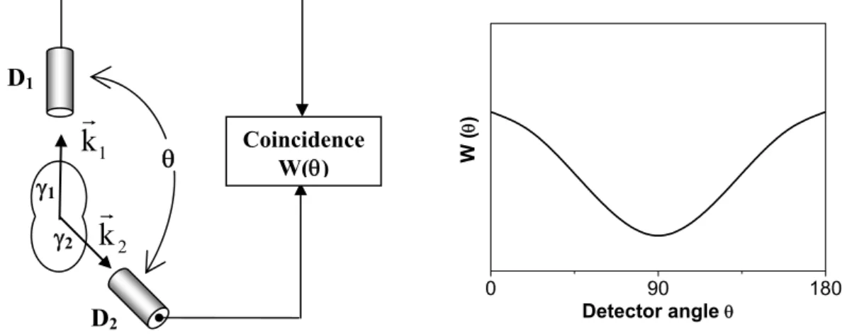
The ZnO sample’s crystalline quality, as well as, the implanted dopants diffusion and lattice defect recovery were evaluated using the Rutherford Backscattering/Channeling technique (RBS/C). With Photoluminescence (PL), the optical activation of the dopant was addressed. The lattice site location of the dopant and its local environment inside the ZnO lattice were studied by means of Emission Channeling (EC) and Perturbed Angular Correlations (PAC), respectively.
Given the extensive number of publications available among the scientific community with a thoughtful explanation of the above referred techniques, in what follows only their main experimental and theoretical features are presented.
2.1. Rutherford Backscattering Spectroscopy
Rutherford Backscattering Spectroscopy/Channeling (RBS/C) is a non-destructive technique based on the elastic collision of an incident particle with a target nucleus, during which an energy transfer occurs, from the particle to the nucleus. The amount of energy transferred depends on the nature of the target nucleus. Therefore, by measuring the energy of the dispersed particle the identity of the target nucleus can be known. Moreover, the final energy of the dispersed particle is also an indication of the depth at which the
28 2.1. Rutherford Backscattering Spectroscopy collision took place. This means that a depth profile of the analyzed sample can be determined. Further information can be extracted from the RBS/C spectra, such as, surface composition, concentration profiles and film thickness. All these factors make of this technique a powerful tool in the field of materials characterization.
2.1.1. General aspects
Figure 2.1 (a) illustrates the above referred basic principles for a composed sample
AmBn where A is heavier than B.
Figure 2.1 – Dispersion geometry and resulting experimental spectrum for a composed sample AmBn.
In this example, an incident particle with initial energy E0 looses energy and is
dispersed by interacting with the atoms of the sample. This interaction can occur immediately at the surface or at a given depth t. In the simplest case of surface interaction,
the particle is scattered by an angle θ = 180º-θ1-θ2 and will have a final energy of KAE0 or
KBE0 depending on whether it collided with atom A or atom B, respectively. KA (or KB)
represents the kinematic factor, given by the quotient between the final energy of the particle and its initial energy in an interaction with atom A (or B). It characterizes, therefore, the energy lost on the collision. By making use of the laws of energy and linear momentum conservation the kinematic factor depends only on the masses of the incident particle and of the target nucleus, as well as on the dispersion angle. For the case of a collision with atom A we get [1],
KA = 2 A p 2 2 p 2 A p 0 f M M θ sin M M cosθ M E ) ( E ⎟⎟ ⎟ ⎠ ⎞ ⎜⎜ ⎜ ⎝ ⎛ + − + = A (2.1) E0 θ1 KAE0 KBE0 θ2 KAE KBE θ t E Ef (A) = KAE0 - ΔEA Ef (B) = KBE0 - ΔEB Yield Energy KBE0 KAE0 A B HA,0 HB,0 HB θ Ef (A) Ef (B) ΔE (B) ΔE (A) Detector a) b)

![Figure 1.2 – Projections along the main symmetry crystallographic directions of ZnO ([0001], [1102], [1101]](https://thumb-eu.123doks.com/thumbv2/123dok_br/15462510.1031438/28.892.108.770.294.783/figure-projections-main-symmetry-crystallographic-directions-zno.webp)

![Figure 2.3 – RBS spectra for 2 MeV 4 He particles from a as-grown ZnO single-crystal (top): a) beam along a random direction and b) beam along the [0001] direction](https://thumb-eu.123doks.com/thumbv2/123dok_br/15462510.1031438/47.892.213.667.127.795/figure-spectra-particles-single-crystal-random-direction-direction.webp)