EFFICIENT TIMING ELEMENT
DESIGN FEATURING LOW POWER
VLSI APPLICATIONS
P.Nagarajan1, T.Kavitha2, S.Shiyamala3
1,2,3
Associate Professor, ECE Department, School of Electrical and Computing Vel Tech University, Chennai, Tamil Nadu, India
1
[email protected], [email protected], [email protected]
Abstract— In this paper, we propose a novel Low-Power Dual dynamic node and edge triggered (DDNET) flip flop for Featuring Efficient low power applications. Several art of design techniques have been proposed to eliminate large capacitance in the precharge node of the conventional flip-flop, which drives separately by output pull-up, and pull down transistors. Though the pioneer designs which consumes much power and it has been overcome by our special handing techniques. The major aim of this work is to optimize the static current and total power dissipation of the flip-flop, which has designed through DDNET flip flop design. The proposed designs which outperforms the existing designs in terms of reduction of total power Dissipation and static current. The proposed DDNET flip flop design provides a power reduction up to 7.1% and 6.4% compared to the conventional flip-flops at 20% and 35% data activities, respectively. The performance of proposed timing element design is analyzed by simulating the element (Flip flop) circuit at 180nm CMOS process technology. The simulation evaluation outcome shows that, the proposed design (DDNET) achieves less number of transistor count up to 30-40% than the conventional method, In addition the Improvement of Power Energy Product (PEP) up to 30-34% and 5-10% reduction in static current Compared to the dual dynamic node hybrid flip-flop. Futher, In this work design and simulation of a 5 MHz, divide-by-2 frequency divider based upon DDNET logic flip-flops in 180 nm CMOS technology are presented. The performance improvements specify that the proposed Designs are appropriate for modern high-performance designs where power dissipation is of major Concern.
Keyword-DDNET, flip flops, static current, low power, frequency divider.
I. INTRODUCTION
At present scenario, technology and speed are constantly moving ahead from low scale integration to large VLSI and from megahertz (MHz) to gigahertz (GHz). The structure necessities are also going up with this uninterrupted advancing process of technology and speed of operation. In synchronous systems, high speed has been achieved using advanced pipelining techniques. In modern deep-pipelined architectures, power dissipation terms to be the major drawback. This overhead in the present architecture is the static current and power dissipation associated with the pipeline elements, such as the flip-flops and latches. Far-reaching work has been dedicated to get better the performance of the flip-flops in the past few decades [1]–[3], [8]–[11], [12]. The Classic high-performance flops are discussed in Hybrid latch flop (HLFF) [1] and semi dynamic flip-flop (SDFF) [2]. The qualities of dynamic and static structures are combined through hybrid architecture. Besides,[3], shows that the SDFF has a characteristic capability of incorporating logic very efficiently, because unlike the true single-phase latch (TSPC) in their experiment work. This greatly helps in reducing the pipeline overhead since the delay and area associated with one or more logic stages preceding the flip-flop can be eliminated. Several hybrid flip-flop designs have been proposed in the past decade, all aiming at reduction of power, delay, and area [8]–[11].Flip-flop architecture named cross charge control flip-flop (XCFF) [4], which has substantial advantages over SDFF and HLFF in both power and speed. It uses a split-dynamic node to reduce the precharge capacitance, which is one of the major significant reasons for the large power dissipation in most of the conventional designs. Power dissipated to drive the input of the flip flop is due to switching power, short-circuit and leakage power.[11]
Power P P P (1)
Switching Activity Factor: α
If the signal is a clock, α = 1 then If the signal switches once per cycle, α = ½.besides For Dynamic gates: switch is either 0 or 2 times per cycle, α = ½ and for the Static gates: depending on design, but typically α = 0.1
P a. f. C . V
Short-circuit power occurred when there is a transition between VDD and GND occurs
P I . V . f
P f V , V , W L⁄
However, this structure still has some demerits, due to redundant power dissipation that results when the data does not switch for more than one clock (CLK) cycles. In addition, the large hold-time requirement makes the design of timing-critical systems with XCFF an involved process. The major aim of this research work is to optimize the total power dissipation of the flip-flop design, which has designed via DDNET .This method that eliminates the drawbacks of XCFF. The new designs are free from unwanted transitions resulting when the data input is stable at zero. DDNET architecture reduces the static current and power dissipation of the flip-flop. The performances of proposed modern high performance flip-flops architecture are compared with that of dual dynamic node hybrid flip-flop (DDFF) different data activity and power factor.
The rest of this paper is divided as follows. Section II projects the state-of-the-art flip-flop architectures and discusses the drawbacks of the existing flip-flop architectures and challenges in achieving high performance. In Section III, the proposed DDNET (Design D1 and Design D2) architecture and its operations are discussed. In Section IV, Description about frequency application is analyzed for proposed method. In Section V, we present the performance analysis methods to compare the proposed architectures with conventional designs. Then the results of various performance comparisons, including Power, PDP, Energy delay product (EDP), Power Energy product (PEP) and static current, are provided. Finally, in Section IV, we bring to a close conclusion.
II. CONVENTIONALMETHODS
Past few years enormous number of flip-flops and latches where published which are categorized under static and dynamic styles. The master – slave flip-flop with transmission gates and PowerPC 603 master-slave include the former designs of mater – slave flip-flop. The delay overhead associated with latching elements are expressed as data –to – output delay preferably than clock –Q delay. The grand of setup – time and CLK –Q delay of the flip – flop forms the D- Q delay. Previous static designs lack D-Q delay due to large positive setup time liable to be influenced by clock overlap. One among the methodological static structure with the advantage of low –power keeper structure and latency direct path includes the PowerPC603 when not considering speed. The disadvantages of this design include large positive setup resulting in D-Q delay along with large data and clock node capacitance reducing the performance of the design.
Fig.1. Dual dynamic node hybrid flip-flop
As shown in Fig.1.The (dual dynamic node hybrid flip-flop)[1] DDFF architecture displays negative setup time since the short transparency period defined by the 1–1 overlap CLK of and CLKB allows the data to be sampled even after the rising edge of the CLK before CLKB falls low.
III. PROPOSED METHODOLOGIES
From the background work following methods POWER PC, HLFF, semi dynamic, CDMFF flip-flop is used which divide dynamic node to reduce the pre-charge capacitance, which consumes power in most of the conventional designs. In order To overcome the large power dissipation in DDFF architecture which removes incorporate complex logic functions in the flip-flops.In DDFF the data holding time which increase the Delay in turn introduce large power dissipation. This leads to a small negative setup time and a positive hold time close to zero. The drawback has been overcome by the proposed DDNET (D1 and D2). In which the data activity does not switch for more than one clock (CLK) cycle would be the major merit of this design. The proposed method DDNET-D1 & DDNET-D2, DDNET stands Dual dynamic node and edge triggered.
A. DDNET-D1
In DDNET-D1 is designed based on C2 MOS logic. It is constructed by totally 12 numbers of transistors. In existing method clock activity is based on single edge triggering and it is controlled through Mp1, Mn1, Mn2, and Mn4 transistor as shown in the Fig.1.Apart from that it also depends on the input data which is passed on to Mn2 transistor. Though DDFF requires four transistors for clock activity. The proposed (DDNET-D1) design requires two transistors Mp1 and Mn2 for clock activity. Hence the proposed design has less clock activity than DDFF design. The operation of this design is based on the activity of clock, C2MOS design will be activated and produce output through keeper circuit, whenever there is a switching activity occurs between CLK & data .The elimination of redundant internal transitions is done across Differential inputs configuration which results data activity is of low latency and the reduced insertion power overhead when compare to existing DDFF. Switching activity occurs between CLK & data (“low” and “high”) are different and it activates Mp3, Mn3 and generates the Q output. If D changes from 0 to 1, when CLK is high, the pull up network will be disconnected by MP2 using data mapping scheme (MN2 turns off MP2).
d
MP1
MN3 MN2 MN1
+ clk
clk
gnd
gnd gnd vdd
MP2
MP4 gnd vdd
gnd vdd
MP3
MP5
qb
Fig.2.Dual dynamic node and edge triggered-D1
If D changes from 1 to 0, the pull down network is disconnected from the GND, besides PMOS transistor MP3 will be partially on, and a glitch will appear at output node Q. An attempt to decrease the transparency period results in a larger size of the transistors in this path, which ensuing higher capacitance on node X2 As shown in the Fig.2.and hence it has higher power dissipation. Hence, in the proposed DDNET-D1 structure the internal node is not connected with Vdd to GND during the clock activity. During these switching transmissions, the circuit is at float, which holds the data and capacitance discharge with high speed. In existing method (DDFF) consistent switching activity occurs in weaker keeper circuit which in turn keeps the Mp2 and Mp3 transistor ON which increases switching activity of the stronger keeper circuit at the output node. These operation overheads the power dissipation is at the output node. In our proposed design weaker keeper circuit is replaced and the transistor Mp3, Mn3 is controlled by input data. This helps to reduce unwanted switching activity in the stronger keeper circuit at the output node. This facilitates the power dissipation lesser when compared to conventional DDFF.
B. DDNET-D2
In DDNET-D2 is designed using pseudo-dynamic structure without weaker keeper inverter at X1 node as shown in the Fig.3. It is constructed by totally 14 numbers of transistors. In DDNET-D1 design the clock. Activity is depends on input data but in DDNET-D2 the clock activity doesn’t depend on input data because the data is passed in both input node as well as to the source of Mn3 and Mn6 simultaneously. This helps to reduce the clock activity than DDNET-D1 design. Data for the signals which generated from X1 node are directly connected to the NMOS. At that case when the signal is “high” the NMOS, which connects to node X2, pull down the Data value and captured in inverter node Q.
Fig.3.Dual dynamic node and edge triggered-D2 MP1
MN2 MN1
MP2
gnd gnd vdd
gnd vdd
gnd
gnd
gnd Vdd
MN6 MP4
MP3
Vdd
MN3 MN4 MN5 clk
qb
D
Q MP1
MN2 MN1 MP2
gnd gnd
vdd vdd
KEEPER
MP3 vdd
gnd clk
IN
MN3
b
In PMOS transistor, the two weak NMOS which connects node X2 transistors effectively, which helps to avoid the floating occurs in Mn3 and Mn6. So that the flip-flops will not at be clear, thereby providing a fully static operation. The explicit pulse generated from X1 node makes the PMOS transistor off which makes the X2 node low which in turn stops the data activity at input node, which is connected at X2, that activates the dual edge triggering based on previous data value and generates output data. Due to this high voltage drop reduced across NMOS transistor.
In PMOS transistor, the two weak NMOS which connects node X2 transistors effectively, which helps to avoid the floating occurs in Mn3 and Mn6. So that the flip-flops will not at be clear, thereby providing a fully static operation. The explicit pulse generated from X1 node makes the PMOS transistor off which makes the X2 node low which in turn stops the data activity at input node, which is connected at X2, that activates the dual edge triggering based on previous data value and generates output data. Due to this high voltage drop reduced across NMOS transistor
In DDNET-D1 strong keeper circuit, Mp3, Mn3 and inverter (Total number of transistor=8) swings with respect to clock and input data. But in DDNET-D2 design once the node X2 goes high Mn3, Mn6 and inverter gets activated (Total number of transistor=4) and in contrast when X2 node goes low Mn4, Mn5, Mp3, Mp4 transistors are activated (Total number transistor count=4).As transistor switching activity is reduced through X2 node(Based on High and Low condition) the Data holding and switching activity at capacitor discharge with high speed that helps to reduce the latency and power dissipation compared to DDNET-D1 Design. Besides in order to analyze the performance further both the designs are implemented and checked with frequency divider application.
IV. FREQUENCY DIVIDER
The performance improvements specify that the proposed Designs are appropriate for modern high-performance designs where power dissipation is of major Concern. The proposed design is implemented in Frequency Divider component which produces an output based on the clock input divided by the specified value. In this design we specified Frequency divided by 2. Design and simulation of a 5 MHz, divide-by-2 frequency divider based on DDFF and DDNET logic flip-flops in 180 nm CMOS are Presented. The Frequency Divider internally uses an N-bit counter synthesized in digital logic’s, where N is the smallest integer. This counter value is compared to the Divider parameter and the High Pulse Time parameter to produce the divide output value. As shown in the Fig.4 and Fig.5).
In our design flip flop designs are implemented in FD. It consists of MUX Design, to control the output based on selection. MC (mode control signal) is low, and the added transistors do not affect the behavior of the MUX2. When MC goes high, the path from the output of the flip flop 2 to the node is enabled. Once OUT goes high, the added path forces to MUX which select logic low and extend the high level of the flip flop 1 output. Therefore, the division ratio becomes 2 at out node. The comparison of various parameters is analyzed for this design in section V.
Fig.4.Frequency divider based on DDNET-D2
FD
clk
MUX
IC
MUX
S
FD
clk
OUT
Fig.5.Frequency divider based on DDNET-D1
V. PERFORMANCE ANALYSIS AND RESULTS COMPARISON
We use 180-nm CMOS transistor model in the simulations. The nominal supply voltage of the model is 1.8 V. The CLK driving power is found as the difference in flip-flop design with weaker keeper circuit and without keeper circuit. Similar method is used to find the data driving power, where X2 node in the DDNET-D2 is considered. The Simulations and leakage analyses are performed at 1.8 V supply voltage at room temperature. The design and simulation of a 5 MHz, divide-by-2 frequency divider based on DDFF and DDNET logic flip-flops in 180 nm CMOS are Presented. The DDNET-D1 and DDNET-D2 with are simulated under similar conditions to accurately extract the average power dissipation. This is calculated using
p vdd.
Where Vdd is the supply voltage, Idd is the supply current, and T is the period.Isc the short circuit current and f indicates the frequency Power dissipation at the internal node of the flip-flop, which includes the dynamic power used up on local stage CLK processing, power on the dynamic nodes, and the static leakage power. Comparison on Energy delay product (EDP), Power delay product (PDP), static current.PEP and power dissipation of various conventional flip-flop methodologies at 20% to 35% data activity as shown in the Table I, II and III. Besides the complete analysis has made and all designs have been optimized using DDNET (D1 and D2) design.
The results show that the conventional counterparts have the lowest PDP among the group. As the static power, dissipation is reduced by controlling the switching activity of the transistor. The power comparison for various styles due to switching activity has shown in Table IV and Fig.6.The output of the flip-flop (D-to-Q) determines the time required for a data value to Appear at the output stage. We calculated the timing parameter CLK-to-Q, since D-to-Q Latency depends on when the data transition occurs. In particular data changes with respect to clock edge, the proposed method is the most attractive choice. For example, when clock activity rate is 0.5 and data activity for single end flip-flop (FF) is same as input for the positive edge of the clock and unequal at the negative edge. In case of double end FF the data activity is same as input data for both the edges.
At 25% data activity, CDMFF dissipates lowest power because the conditional Structure eliminates the outmoded transitions. However, as the data activity increases CDMFF dissipates moderately higher power because of the higher power dissipation in the conditional structures. In view of the fact that this redundancy is eliminated, DDNET provides better-quality performance for this data pattern.
As shown in the Fig.8.The leakage current is a function of the bias condition of source, drain, gate and body of each transistor. Hence, the total static power dissipation of the flip-flop depends on the state of the input and output terminals. The flip-flop dissipates the lowest leakage power is due to the dissipation of flip-flop transistors are biased in the least leakage condition. Note that DDNET design has least amount leakage power dissipation among the compared designs. This corresponds to CLK = 1, D = 0, and Q = 1 and CLK = 1, D = 1, and Q = 1 states.
HLFF has superior leakage performance for almost all input-output states. We believe that the remarkably smaller variation in leakage power with changing input-output state vector in HLFF and CDMFF is due to the larger stack of transistors in these designs. Because it needs 20 to 25 transistor for crafting the design. The PowerPC has the highest maximum leakage power for an input-output state CLK = 1, D = 0, and Q = 1.And it needs 20-22 transistors. It is interesting to note that the same state vector causes the largest leakage in one design and the least in another. For instance if we consider PDP and EDP there would be contrast in existing and proposed design.
FF
cl
k
MUX
MC
MUX
S
FF
cl
k
TABLE I. Parameter Comparison Table for Background Flip-Flop Structures
PARAMETER POWER PC603 HLFF SEMIDYNAMIC CDMFF
No. of. transistors 22 20 23 21
Static current (uA) 0.6987 1.2390 2.0302 1.8699
Max power (uw) @ time
1.2578 @ 4.00142e-006
2.2303 @ 1.001e-006
3.65438 @ 5.001e-006
3.36593 @5.001e-006
PDP (pj) 5.0329 2.2325 18.2755 16.8330
EDP(js*10-17 ) 2.0139 0.2234 9.1396 8.4181
PEP(jw*10-18) 6.3303 4.9780 66.7856 56.8280
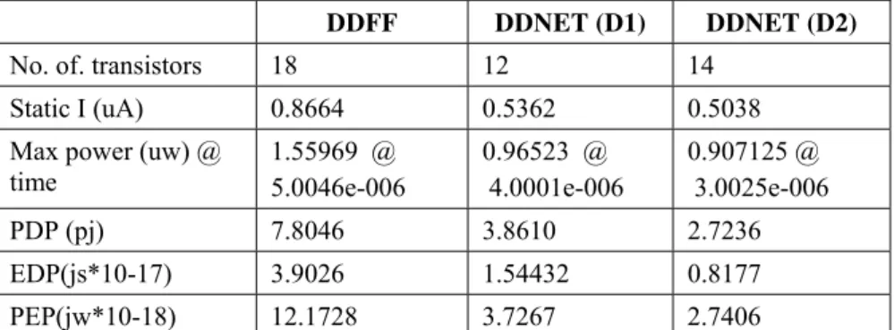
TABLE II. Parameter Comparison Table for Proposed and Conventional Counterpart
DDFF DDNET (D1) DDNET (D2)
No. of. transistors 18 12 14
Static I (uA) 0.8664 0.5362 0.5038
Max power (uw) @ time
1.55969 @ 5.0046e-006
0.96523 @ 4.0001e-006
0.907125 @ 3.0025e-006
PDP (pj) 7.8046 3.8610 2.7236
EDP(js*10-17) 3.9026 1.54432 0.8177
PEP(jw*10-18) 12.1728 3.7267 2.7406
TABLE III. Parameter Comparison Table for Frequency Divider for Proposed Method
PARAMETER FD-DDNET (D1) FD-DDNET (D2)
Max power (uw) @ time
16.66532@ 15.001e-006
13.9174@ 12.001e-006
PDP (j*10-10) 2.4999 1.6704
EDP(js*10-15) 3.7501 2.0049
PEP(jw*10-15) 4.1661 2.3248
Frequency (MHz) 5 5
TABLE IV. Power Comparison Table for Proposed and Conventional Counterpart
Circuit Power Dissipation (uw)
POWER PC603 1.25766
HLFF 2.23022
SEMIDYNAMIC 3.65436
CDMFF 3.36582
DDFF 1.55952
DDNET (D1) 0.96516
DDNET (D2) 0.90687
The proposed method has 6.4% - 7.1% Reduction in total power dissipation compared to PowerPC, XCFF, SDFF and DDFF respectively, along with comparable speed performance. In Addition, it gives power performance comparable to CDMFF while providing improvement in PDP. SDFF and PowerPC have the highest CLK power dissipation, whereas the proposed DDNET (D1 and D2) has the least. PowerPC and CDMFF dissipate the highest data driving power. The DDFF exhibits a smaller negative setup-time compared to SDFF and HLFF.
power dissipation (Table I). In DDNET-D1 8 transistor are required for constructing strong keeper circuit, Mp3, Mn3 and inverter which is responsible for the swings occur at clock and input data. But In DDNET-D2 design when X2=1 the transistors Mn3, Mn6 and inverter gets activated in turn these 4 transistors which reduces half of the switching activity than DDNET-D1 and in contrast when X2 =0 another 4 transistors Mn4, Mn5, , Mp3, Mp4 transistors are activated. As transistor switching activity is reduced half through X2 node(Based on High and Low condition) the Data holding and switching activity at capacitor discharge with high speed that helps to reduce the latency and power dissipation compared to DDNET-D1 Design. As the total power dissipated in the
flip-flop depends on the clock and data activity, an illustration of power dissipated at data activities where X2 node in the DDNET-D2 is considered. The results demonstrate that the proposed DDNET design consumes lowest total power for 20% to 35% data activity. As DDNET-D2 is constructed by totally 14 numbers of transistors. In DDNET-D1 design the clock Activity is depends on input data but in DDNET-D2 the clock activity doesn’t depend on input data because the data is passed in both input node as well as to the source of Mn3 and Mn6 simultaneously. This helps to reduce the clock activity than DDNET-D1 design. As mentioned prior, the small precharge node, CLK-input, and data-input capacitances makes the planned DDNET (Design D1 and Design D2) flip-flop power efficient at higher data rates. Besides, it gives advanced geometric weight to power than delay and produces lower power solution than the other two Matrices. The conventional design metrics to minimize the both power and delay of the electronic designs is power delay product PDP. If D represents delay and P represents power consumption of the circuit then the metric can be expressed as PDP (energy) = Power (P)×Delay (D). We also estimate the PDP (Power Delay Product) by multiplying power dissipation with average D-to-Q.
Fig.6. Comparison on power dissipation of various flip-flop designs
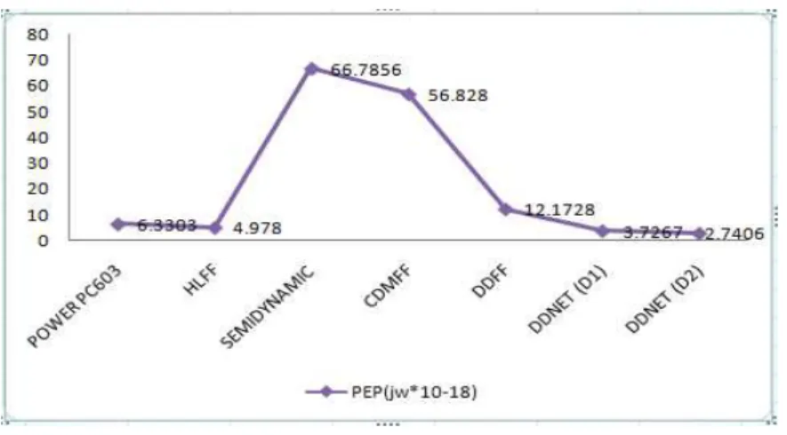
Fig.8. Comparison of Static PEP for various styles
But it may not be appropriate when the low power dissipation is priority. The three foremost sources of energy utilization in a flipflop is input energy, which represents the energy dissipated to drive the input of the
flipflop, clock energy, the energy dissipated at the internal nodes, internal energy the energy dissipated in the local clock buffer driving the clock. The most significant actuality about the energy dissipation of a flipflop is the function of input activity, besides also a function of clock activity. Energy can be saved by gating the clock, as is commonly done in proposed low-power designs. [17], [18]. But it may not be appropriate power dissipation.
Fig.9. Comparison of Optimized parameters various styles
Would be the major concern. This metric is more suitable when the performance is the main concern. If power is the higher priority than both EDP and PDP matrices may not provide better solutions.
It gives higher geometric weight to power than delay and produces lower power solution than the other two matrices. It is expressed as PEP = Power Energy; PEP = P×P×D. The three matrices are analyzed for proposed design. The timing element proposed here is power Efficient. For that the PEP is considered as a circuit optimization parameter. The proposed circuits were optimized for Power Energy Product (PEP). It is articulated in the Table. I and II and Fig.8.
Specifies that the proposed low-Power Dual dynamic node and edge triggered Designs are suitable for modern high-performance designs where power dissipation is of foremost Concern.
VI. CONCLUSION
In this work, a new low power timing element DDNET-D1 and DDNET-D2 were proposed. An analysis of the overlap period requisite in selecting proper switching activity of clock and data was provided in order to formulate the design process simpler. The proposed DDNET-D2 design which efficiently halves the switching activity of clock and data which results low power dissipation than DDNET-D1 and DDFF. A comparison of the proposed flip-flops with the conventional flip-flops showed that it exhibits lower power dissipation and static current along with comparable speed performances by reducing number of transistor count. The post-layout simulation results showed an improvement in PEP by about 30-34% compared to the DDFF design at 20-35% data activity. By eliminating the unwanted switching activity in, the revised structure of the proposed (DDNET-D2) flip-flop, is capable of efficiently incorporating complex logic in to the flip-flop. The presented DDNET-D2 outperforms the DDNET-D1 and DDFF in the CLK driving power and in internal power dissipation. The EDP and PDP variation performances of the flip-flops were studied in detail. The efficiency of the flip-flop was further highlighted by using divide-by-2 frequency divider which operated in 5MHz, respectively. It was verified that the proposed architectures are well appropriate for present high-performance designs where power dissipation is of foremost concern.
REFERENCES
[1] Kunwar Singh, Satish Chandra Tiwari, and Maneesha Gupta, “A Modified Implementation of Tristate Inverter Based Static Master-Slave Flip-Flop with Improved Power-Delay-Area Product”, Hindawi Publishing Corporation Scientific World Journal Volume 2014, Article ID 453675.
[2] Kalarikkal Absel, Lijo Manuel, and R.K.Kavitha, Member, IEEE Low-Power Dual Dynamic Node Pulsed Hybrid, IEEE transactions on very large scale integration (VLSI) systems, vol. 21, no. 9, Sep, 2013.
[3] A.Hirata, K. Nakanishi, M. Nozoe, and A. Miyoshi, “The cross charge-control flip-flop: A low-power and high-speed flip-flop suitable for mobile application SoCs,” in Proc. Symp. VLSI Circuits Dig. Tech. Papers, Jun. 2005, pp. 306–307.
[4] B. S. Kong, S. S. Kim and Y. H. Jun, Conditional-capture flip-flop for statistical power reduction IEEE J. Solid-State Circuits, vol. 36, no. 8, N pp. 1263–1271, Aug. 2001.
[5] C. K. Teh, M. Hamada, T. Fujita, H.Hara, N. Ikumi, and Y. Oowaki, Conditional data mapping flip-flops for low power & high-performance high-performance systems IEEE Trans. (VLSI) Syst., vol. 14, no. 12, pp.1379–1383, Dec. 2006.
[6] C. Cao, A power efficient 26-GHz 32:1 static frequency divider in 130-nm Bulk cmos IEEE Microw. Wireless compon. Lett., vol. 15, no. 11, pp.721–723, Nov. 2005.
[7] F. Klass, “Semi-dynamic and dynamic flip-flops with embedded logic,” in Proc. Symp. VLSI Circuits Dig. Tech. Papers, Honolulu, HI, Jun. 1998, pp. 108–109.
[8] F. Klass, N. Nedovic, M. Aleksic, and V. G. Oklobdzija, “Conditional pre-charge techniques for power-efficient dual-edge clocking,” in Proc. Int. Symp.Low-Power Electron. Design, 2002, pp. 56–59. “Semi-dynamic and dynamic flip-flops with embedded.
[9] G. Gerosa, S. Gary, C. Dietz, P. Dac, K. Hoover, J. Alvarez, H. Sanchez, P. Ippolito, N. Tai, S. Litch, J. Eno, J. Golab, N. Vanderschaaf and J. Kahle, “A 2.2 W, 80 MHz superscalar RISC microprocessor,” IEEE J. Solid-State Circuits, vol. 29, no. 12, pp. 1440–1452, Dec. 1994.
[10] Patrovi, R. Burd, U. Salim, F. Weber, L. DiGregorio, and D. Draper, “Flow-through latch and edge-triggered flip-flop hybrid elements,” in Proc. IEEE ISSCC Dig. Tech. Papers, Feb. 1996, pp. 138–139.
[11] J. Yuan and C. Svensson, “New single-clock CMOS latches and flipflops with improved speed and power savings,” IEEE J. Solid-State Circuits, vol. 32, no. 1, pp. 62–69, Jan. 1997.
[12] J. M. Rabaey, A. Chandrakasan, and B. Nikolic, Digital Integrated Circuits: A Design Perspective, 2nd ed. Englewood Cliffs, NJ: Prentice-Hall, 2003.
[13] M. Alioto, R. Mita, and G. Umbo, “Design of high speed MOS current Mode logic frequency dividers,” IEEE Trans. Circuits Syst. II, Exp. Briefs, vol. 53, no. 11, pp. 1165–1169, Nov. 2006.
[14] N. Nedovic, M. Aleksic, and V. G. Oklobdzija, “Conditional pre-charge techniques for power-efficient dual-edge clocking,” in Proc. Int. Symp. Low-Power Electron Design, 2002, pp. 56–59.
[15] P. Zhao, T. K. Darwish, and M. A. Bayoumi, “High-performance and low-power conditional discharge is flip-flop,” IEEE Trans. Very Large Scale Integr. (VLSI) Syst., vol. 12, no. 5, pp. 477–484, May 2004.
[16] V. Stojanovic and V. Oklobdzija, “Comparative analysis of master-slave latches and flip-flops for high-performance and low-power sys-tems,” IEEE J. Solid-State Circuits, vol. 34, no. 4, pp. 536–548, Apr.1999.
[17] P. Nagarajan, R. Saravanan & P. Thirumurugan 2014 “Design of register element for low power clocking system”, Information-An International Interdisciplinary Journal, vol.17, no.6(B), pp.2903-2913