Abstract—This paper presents a self-checking implementation for adder schemes using the dual duplication code. To prove the efficiency of the proposed method, the circuit is simulated in double pass transistor CMOS at 32nm technology and some transient faults are voluntarily injected in the layout of the circuit. This fully differential implementation requires only 20 transistors which mean that the proposed design involves 28.57% saving in transistor count compared to the implementation using standard CMOS technology.
Index Terms—full adder, double pass transistor technology, self-checking, faults
I. INTRODUCTION
Addition is one of the fundamental arithmetic operations. It is used extensively in many VLSI systems such as microprocessors and application specific DSP architecture. In addition to its main task, which is adding two numbers, it is the nucleus of many other useful operations such as, subtraction, multiplication, address calculation, etc [1, 2]. As a result, design of a high-performance full-adder is very useful and important [3, 4, 5-6] to ameliorate the performance of overall modules. This is the reason of many researchers trying to present different logics of 1-bit full adder [7-8].
The most conventional one is complementary CMOS full adder (C-CMOS) [9]. It is based on regular CMOS structure with pull-up and pull-down transistors and has 28 transistors.
Another conventional adder is the Complementary Pass-Transistor Logic (CPL) [10, 11, 12] with swing restoration which uses 32 transistors. CPL produces many intermediate nodes and their complement to make the outputs. The basic
Manuscript received December 09, 2011; revised 2012.
K. Chiraz and K. Mouna are with the Electronic & Microelectronics Laboratory, Monastir Tunis University, Tunisia. Email: {chirazkhedhiri, mouna.karmani}@yahoo.fr
H. Belgacem is with the Electronic & Microelectronics Laboratory, Monastir Tunis University and ISSAT, Sousse, Tunisia. Email: [email protected]
K.L. Man is with the Xi'an Jiaotong-Liverpool University, China, Myongji University, South Korea and Baltic Institute of Advanced Technology, Lithuania. Email: [email protected]
Yue Yang and Lixin Cheng are with the Suzhou Institute of Nano-Tech and Nano-Bionics, Chinese Academy of Science, China. Email: {yyang2010, lxcheng2011}@sinano.ac.cn
The research work presented in this paper is partially sponsored by SOLARI (HK) CO (www.solari-hk.com) and KATRI (www.katri.co.jp and www.katri.com.hk).
difference between the pass transistor logic and the complementary CMOS logic styles is that the source side of the pass logic transistor network is connected to some input signals instead of the power lines [13, 14]. A Transmission Gate Full-Adder (TGA) presented in [15] contains 20 transistors.
Double pass transistor full adder cell has 48 transistors and operation of this cell is based on the double pass transistor logic in which both NMOS and PMOS logic networks are used [16].
On the other hand, the design of a faster and highly reliable adder is of major importance. Thus, much effort has been invested in the research that has led to faster and more efficient ways to perform this operation [17, 18].
Fault tolerance allows a reliable system operation in the presence of errors [19, 20]. While classical fault tolerant architectures such as triple modular redundancy (TMR) are very costly, self-checking circuits provide an interesting alternative [21, 22]. Self-checking circuits consist of a functional unit encoded by means of an error detecting code and are continuously verified by the checker [23]. Typically, computed results are verified by using a self-checking design technique, primarily because the self-checking property allows both transient/intermittent and permanent faults to be detected, thus preventing data contamination.
That is why from the very early developments of fault tolerant computers, an important amount of effort had been done on designing self-checking arithmetic units. The first ones are based on arithmetic residue codes [24-25]. Then a parity prediction scheme has been proposed in [26] and [27]. A Berger code prediction scheme has been also developed in [28], and more recently self-checking fully differential design has been proposed [29].
In this paper, we present a self-checking full adder based on two-rail encoding scheme. To prove the efficiency of the proposed method, the circuit is simulated in double pass transistor CMOS 32nm technology and some transient faults are voluntary injected in the layout of the circuit. The proposed design involves 28.57% saving in transistor count compared to standard CMOS technology.
The paper is organized as follows. In Section II, we describe the proposed design. Section III shows the simulation results in 32nm double pass transistor process technology. Conclusions are given in Section VI.
A Self-checking CMOS Full adder in Double
Pass Transistor Logic
Chiraz Khedhiri, Mouna Karmani, Belgacem Hamdi, Ka Lok Man, Yue Yang and Lixin Cheng
Proceedings of the International MultiConference of Engineers and Computer Scientists 2012 Vol II, IMECS 2012, March 14 - 16, 2012, Hong Kong
ISBN: 978-988-19251-9-0
ISSN: 2078-0958 (Print); ISSN: 2078-0966 (Online)
II. PROPOSEDDESIGN
The blooming development of Computer Science has led to the growth of Integrated Circuit (IC) devices. Most of the Very Large Scale IC (VLSI) applications, such as digital-signal processing and microprocessors, use arithmetic operations extensively [30]. In addition, among these widely used operations, subtraction and multiplication are most commonly applied. The 1-bit full adder is the building block of these operation modules.
A full adder is a three-input two-output block, where the inputs are the two bits to be summed: a and b, and the carry input bit (Cin), which derives from the calculations of the
previous digits. The outputs are the result of the sum operation, Sum, and the resulting value of the carry output bit (Cout) [31].
Many full adders have been designed and published in literature. They are built upon different logic styles [32].
In this paper, we present a self-checking full adder based on the double pass transistor technology.
A. Double pass-transistor logic (DPL)
The basic difference of pass transistor logic compared to the CMOS logic style is that the source side of the logic transistor networks is connected to some input signals instead of the power lines. In the Double Pass Transistor Logic (DPL) style [33, 34, 35], both NMOS and PMOS logic networks are used in parallel.
Pass transistor logic is attractive as fewer transistors are needed to implement important logic functions, smaller transistors and smaller capacitances are required, and it is faster than conventional CMOS. However, the pass transistor gates generate degraded signals, which slow down signal propagation. This situation will be more critical when the output signals should be propagated to next stage as is the case for the carry gate in ripple carry adder.
To avoid this signal degradation, inverters are added in the outputs of the circuit.
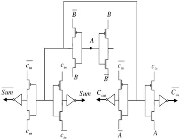
In Fig. 1, the schematic of the proposed static DPL logic circuit for a full adder is shown.
B
B B
B
A
in
c cin
in
c
in
c
Sum Sum
in
c cin
A A
out
C Cout
Fig. 1. The proposed self-checking full adder
Inverters are added to restore degraded signals generated by the differential SUM and carry gate.
This fully differential implementation requires only 20 transistors which mean that the proposed design involves 28.57% saving in transistor count compared to standard CMOS technology.
B. Self-checking design
Self-checking circuits are increasingly becoming a suitable approach to the design of complex VLSI circuits, to cope with the growing difficulty of on-line and off-line testing [36]. They are class of circuits in which occurrence of fault can be determined by observation of the outputs of the circuits.
Self-checking circuits are based on an appropriate coding of the inputs and outputs of the circuit. Code checkers are used to monitor whether the circuit responses are within the output code space. As long as this condition is fulfilled, the output is assumed to be correct. If the code checker reveals a non code word, an error is detected [37].
The checker determines whether the output of the circuit is a valid code word or not. It also detects a fault occurring within itself [38]. Double-rail checker is based on the dual duplication code as shown in Fig. 2. It compares two input words X and Y that should normally be complementary (
y
x
) and delivers a pair of outputs coded in dual-rail.Fig. 2. Dual rail checker cell
A self-testing dual-rail checker can be designed as a parity tree where each XOR gate is replaced by a dual rail checker cell. The resulting checker is also an easily testable circuit since only four code inputs are needed to test a dual rail checker of any length [39]. This checker is important in self-checking design since it can be used to check dual blocks (and duplicated blocks by inverting the outputs of one of them). However, its more significant use consists of the compaction of the error indication signals delivered by the various checkers of a complex self-checking circuit. Each checker delivers a pair of outputs coded in dual-rail. Thus, the dual-rail checker can compact the dual-rail pairs delivered by the various checkers of the system into a single dual-rail pair. This pair delivers the global error indication of the system.
III. SIMULATION RESULTS
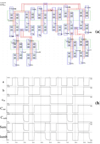
The full adder circuit is implemented in full-custom 32nm DPL technology [40]. SPICE simulations of the circuit extracted from the layout, including parasitic, are used to demonstrate that this adder has an acceptable and expected electrical behaviour.
The SPICE simulation of the differential full adder is as shown in Fig. 3.
Proceedings of the International MultiConference of Engineers and Computer Scientists 2012 Vol II, IMECS 2012, March 14 - 16, 2012, Hong Kong
ISBN: 978-988-19251-9-0
ISSN: 2078-0958 (Print); ISSN: 2078-0966 (Online)
a
b
cin
Cout
Coutb
Sumb Sum
Fig. 3. Differential full adder. (a): Layout and (b): Electrical simulation (SPICE)
As it is shown in Fig. 3(b), the differential outputs are complementary which proves that the circuit is fault free.
In order to verify the circuit’s capability with realistic circuit defects, we simulate the adder in the
presence of faults. Faults are voluntarily and manually injected into the physical layout of the circuit. In this case, the fault is injected in the primary input: (
a
a
). The SPICE simulations are shown in Fig. 4.a
b
cin
Cout
Coutb
Sumb Sum
Fig. 4. SPICE simulation of the adder in 32nm DPL technology with injection of primary fault (aa)
In order to show the importance of the dual rail checker in the detection of faults, we simulate a two bit of the full adder of Fig. 4.
Fig. 5 gives an example of these simulations.
Cout1
Cout2
Coutb1
Coutb2
fCout
fCoutb
fSum
fSumb
Sum1
Sum2
Sumb1
Sumb2
Fig. 5. SPICE simulation of the 2 bits full adder in 32nm DPL technology with injection of a primary fault (aa)
The above simulations show that when the fault is injected into the primary input (a), the duplicated outputs sum (Sum1/Sumb1 and Sum2/Sumb2) and carry (Cout1/Coutb1 and Cout2/Coutb2) do not remain complementary so that checkers (Sum checker and/or carry checker) indicate a non valid code.
In this case, the fault is detected by the outputs of the carry checker. We can see that fCout and fCoutb are not complementary and indicate a non valid code.
IV. CONCLUSION
In this paper, a self-checking full adder is proposed. The circuit is simulated using the double pass transistor logic. This technique involves 28.57% saving in transistor count compared to standard CMOS technology.
The presence of faults in the proposed design is detected using a double rail checker. In the presence of any fault, a non-valid code word is provided as input to the checker yielding a non-valid output code word, hence the fault is detected
.
REFERENCES
[1] Ko, U., P. Balsara and W. Lee, 1995. “Low-power design
techniques for high performance CMOS adders,” IEEE Trans.
Very Large Scale Integr. (VLSI) Syst., (2):327-333.
[2] Song, P.J. and G. De Micheli, “Circuit and architecture trade -offs for high speed multiplication,” IEEE J. Solid-Sate Circuit, 26(9): 1184-1198, 1991.
[3] Junming, L., S. Yan, L. Zhenghui and W. Ling, 2001. “A Novel
10-Transistor Low-Power High- Speed Full Adder Cell, In: Proceedings of IEEE 6th International Conf. Solid-State & Integrated-Circuit Technology, Shanghai Jiao Tong Univ., China, pp. 1155-1158.
[4] Shalem, R., E. John and L. K. John, “A novel low power energy
recovery full adder cell,” In: Proceedings of The Ninth Great
Lakes Symposium on VLSI, Ann Arbor, MI, USA, pp. 380–383, 1999.
[5] Khatibzadeh, A. and K. Raahemifar, “Study and comparison of
full adder cells based on the standard static cmos logic,” In:
IEEE Electrical and Computer Eng. Canadian Conference, pp. 2139-2142, 2004.
[6] Tzartzanis, G. L. S. o. V. N. and W. C. Athas, “Design and analysis of a low-power energy-recovery adder,” In: Proceedings of The Fifth Great Lakes Symposium on VLSI pp. 66- 69, 1995.
[7] H.T. Bui, Y. Wang, Y. Jiang, 2002. “Design and analysis of low power 10 -transistor Full Adders using novel XOR-XNOR
gates,” IEEE Transactions on Circuits & Systems II 49, pp.
25-30. (a)
(b)
Proceedings of the International MultiConference of Engineers and Computer Scientists 2012 Vol II, IMECS 2012, March 14 - 16, 2012, Hong Kong
ISBN: 978-988-19251-9-0
ISSN: 2078-0958 (Print); ISSN: 2078-0966 (Online)
[8] V. Foroutan, K. Navi.M. Haghparast, 2008. “A New Low Power
Dynamic Full Adder Cell Based on Majority Function,” World
Applied Sciences Journal 4, pp. 133-141.
[9] Y. Jiang, A. Al-Sheraidah, Y. Yang, E. Sha and J. G. Chung, “A novel multiplexer-Based Low-Power Full Adder,” in IEEE Trans. on circuits and system II, Vol. 51, No. 7, July 2004, pp. 345-348.
[10] A. Shams, T. Darwish, M. Bayoumi, “Performance Analysis of
Low Power 1-bit CMOS Full-adder Cells,” IEEE Transactions on Very Large Scale Integration (VLSI)Systems, 10(1), 2002 February, 20–29.
[11] C.H. Chang, J. Gu, M. Zhang, “A Review of 0.18 mm Full
adder Performances for Tree Structure Arithmetic Circuits,”
IEEE Transactions on Very Large Scale Integration (VLSI) Systems, 13(6), 2005 June.
[12] S. Issam, A. Khater, A. Bellaouar, M. I. Elmasry, “Circuit
Techniques for CMOS Low-power High-performance
Multipliers,” IEEE Journal of Solid-State Circuits, 31, 1996
October, 1535–1544.
[13] R. Zimmermann, W. Fichtner, “Low-power Logic Styles:
CMOS versus Pass-transistor Logic,” IEEE Journal of Solid -State Circuits, 32 (7), 1997, 1079–1089.
[14] M. M. Vai, “VLSI Design,” CRC, Boca Raton, FL, 2001.
[15] N. Weste, K. Eshraghian, “Principles of CMOS VLSI Design: A
System Perspective,” Addison Wesley, Reading, MA, 1993. [16] M. Suzuki, N. Ohkubo, T.Yamanaka, A. Shimizu, and K. Sasaki,
“A 1.5ns 32b CMOS ALU in double pass-transistor logic,” in Proc. 1993 IEEE Int. Solid-State Circuits Conf., Feb. 1993, pp. 90–91.
[17] Y. Jiang, A. Al-Sheraidah, Y. Yang, E. Sha and J. G. Chung, “A novel multiplexer-Based Low-Power Full Adder,” in IEEE Trans. on circuits and system II, Vol. 51, No. 7, July 2004, pp. 345-348.
[18] K. Navi, M. R. Saatchi and O. Dael, „A High-Speed Hybrid Full
Adder‟, in European Journal of Scientific Research, Vol .26. No.1, 2009, pp. 29-33.
[19] I. Koren and C. M. Krishna, “Fault-Tolerant Systems,” San
Francisco, CA, USA: Morgan-Kaufman Publishers, 2007.
[20] D. K. Pradhan, “Fault Tolerant Computer System Design,”
Prentice Hall, Upper Saddle River, NJ, USA, 1996.
[21] M. Goessel and F. Graf, “Error Detection Circuits,” McGraw -Hill, London, 1993.
[22] M. Nicolaids and Y. Zorian, “On-Line Testing for VLSI – A
Compendium of Approaches,” JETTA, Vol. 12, No. 1-2,
Feb.-Apr. 1998, pp. 7-20.
[23] Goran Lj Djordjevic, Mile K. Stojcev, Tatjana R. Stankovic,
“Approach to partially self-checking combinational circuits
design,” Microelectronics Journal 35 (2004) pp. 945–952.
[24] W. W. Peterson, “On checking an Adder,” IBM J. Res. Develop.
2, April 1958, pp. 166-168.
[25] Avizienis, “Arithmetic Algorithms for Error-Coded Operands,”
in IEEE Trans. on Computer, Vol. C-22, No.6, June. 1973, pp. 567-572.
[26] O.N. Garcia and T.R.Ν. Rao, “On the method of checking
logical operations,” in 2nd Annual Princeton Conf. Inform. Sci.
Sys., 1968, pp. 89-95.
[27] F. F. Sellers, M. Y. Hsiao and L. W. Bearson, “Error Detecting
Logic for Digital Computers,” Mc GRAW-HILL publishers,
New-York, 1968.
[28] M. Nicolaidis, „Efficient implementations of self-checking
adders and ALUs‟, in 23rd International Symposium on Fault-Tolerant Computing, June 1993, pp. 586-595.
[29] M. Lubaszewski., S. Mir, V. Kolarik, C. Nielsen and B.
Courtois, “Design of self-checking fully differential circuits and
boards,” in IEEE Transactions on Very Large Scale Integration
(VLSI) Systems, Volume 8, Issue 2, Apr 2000, pp. 113 -128. [30] J.D. Lee, Y.J. Yoony, K.H. Leez, B.-G. Park, “Application of
dynamic pass- transistor logic to an 8-bit multiplier,” Journal of the Korean Physical Society, Vol. 38, No. 3, March 2001, pp. 220_223.
[31] M. Aliotoa, G. Di Cataldob, G. Palumbob, “Mixed Full Adder
topologies for high-performance low-power arithmetic circuits,” Microelectronics Journal 38. pp. 130–139. 2007.
[32] Pooja Mendiratta & Garima Bakshi, “A Low-power Full-adder
Cell based on Static CMOS Inverter,” International Journal of
Electronics Engineering, 2(1), 2010, pp. 143-149.
[33] N. Ohkubo et al., “A 4.4 ns CMOS 54*54-b multiplier using pass transistor multiplexer,” IEEE J. Solid-State Circuits, vol. 30, pp. 251–257, Mar. 1995.
[34] M. S. Suzukiet a l . , “A 1.5-ns 32-b CMOS ALU in Double Pass-Transistor Logic,” IEEE J. Solid-State Circuits, v o l . 28, no. 11, pp. 1145-1151,November 1993. [35] A. Bellaouar and M. I. Elmasry, “Low-Power Digital VLSI
Design: Circuits and Systems”, Kluwer, Norwell, MA, 1995.
[36] M. Nicolaidis, “On-line testing for VLSI: state of the art and trends,” Integration, the VLSI Journal, Volume 26, Issues 1-2, 1 December 1998, pp. 197-209.
[37] Marc Hunger and Sybille Hellebrand, “Verification and Analysis of Self-Checking Properties through ATPG,” 14th IEEE International On-Line Testing Symposium, Rhodes, Greece, 6 - 9 July 2008.
[38] P. Oikonomakos and M. Zwolinski, “On the Design of Self
-Checking Controllers with Data path Interactions,” in IEEE Transactions on Computers, Volume 55, No 11, Nov 2006, pp. 1423 – 1434.
[39] D. A. Anderson, “Design of self-checking digital networks
using coding techniques”, Univ. Illinois Coordinated Sci. Lab.,
Urbana, IL, Tech. Rep. R-527, Sept. 1971.
[40] E. Sicard, “Microwind and Dsch version 3.1,” INSA Toulouse,
ISBN 2-87649-050-1, Dec 2006.
Proceedings of the International MultiConference of Engineers and Computer Scientists 2012 Vol II, IMECS 2012, March 14 - 16, 2012, Hong Kong
ISBN: 978-988-19251-9-0
ISSN: 2078-0958 (Print); ISSN: 2078-0966 (Online)