Ionically Modi
fied Cellulose Nanocrystal Self-Assembled Films with
a Mesoporous Twisted Superstructure: Polarizability and
Application in Ion-Gated Transistors
Paul Grey,
†,‡Susete N. Fernandes,
†Diana Gaspar,
†,‡Jonas Deuermeier,
†,‡Rodrigo Martins,
†,‡Elvira Fortunato,
†,‡Maria H. Godinho,
†and Luis Pereira
*
,†,‡†i3N/CENIMAT, NOVA School of Science and Technology (FCT-NOVA), Universidade NOVA de Lisboa, Campus de Caparica,
2829-516 Caparica, Portugal
‡CEMOP/UNINOVA, Campus de Caparica, 2829-516 Caparica, Portugal
*
S Supporting InformationABSTRACT: Mesoporous structures made of cellulose nanocrystals (CNCs) and their self-assembly into films are of great interest not only due to their abundancy and sustainability but also due to their ease of chemical modification and nanoscale biomimicry capabilities. However, their implementation in (opto)electronic devices requires further understanding on how these self-assembled twisted mesoporous superstructures respond to electrical stimulus. In this regard, this work focuses on the infiltration of solid CNC droplets with three distinct alkali ions (Li+, Na+, and K+) to
yield films with improved electrochemical response when
compared to pristine ones, while preserving their photonic character. Electrochemical characterization shows capacitances of up to 2.5 μF cm−2 allowing for their integration as solid-state gate electrolytes in amorphous indium−gallium−zinc−oxide transistors, resulting in low operating voltages (<2 V), on/off ratios of up to 6 orders of magnitude, and high saturation mobilities >10 cm2V−1s−1. Devices fabricated on Na+and K+infiltrated CNC films present the best characteristics, indicating pure capacitive charging of the semiconductor. The insights presented here contribute to applications in solid-state ionics in mesoporous structures or the combination of optically active electrolytes capable of providing unique functionalities in ion-gated transistors and circuitry.
KEYWORDS: cellulose nanocrystals, self-assembly, mesoporous structures, ion-gated transistors, photonics
■
INTRODUCTIONThe use of natural materials such as cellulose in electronic devices has shown to be of monumental importance to open up paths to not only cheap but also future-orientated electronic and optoelectronic devices.1,2 The attention gained for its integration as an active or passive component into a big variety of devices can be mainly attributed to its abundance and mass production possibilities, making it one of the cheapest alternatives to replace conventional plastics in the industry.3,4 However, challenges for the integration of conventional paper into optoelectronic devices, such as surface roughness, porosity and opaqueness, remain.5As a consequence thereof attention has shifted to substrates based on cellulose on the nanoscale, showing promising properties including transparency, low surface roughness, and high mechanical strength.6−9 One specific type of nanocellulose, namely cellulose nanocrystals (CNCs), stands out as they have shown intriguing properties for their use as substrates or solid-state electrolytes for electronic devices.10,11When dispersed in water CNCs behave like a lyotropic liquid crystal and give rise to either isotropic or anisotropic suspensions.12 Whereas drying an isotropic
suspension (low CNC concentration) yields transparent films, interesting photonic properties (structural color by iridescence) can be obtained by drying an anisotropic suspension (CNC concentration >2 wt %) because of a twisted ordering on the nanoscale.13This ordering is due to an evaporation-induced self-assembly (EISA) process and is termed a chiral nematic structure.12,14,15 These types of structural colors are ubiquitous in nature. They are found for instance in the characteristic blue wings of the morpho butterfly, certain types of scarab beetles, birds, or even seashells, and they offer potential for their use in highly engineered optical systems.16
The photonic properties that these chiral nematic films develop (such as iridescence and distinct reflection and transmission of left- and right-handed circular polarized light (CPL), respectively) are fascinating and could show potential to be used in exotic applications such as in CPL sensing and
Received: October 5, 2019 Accepted: November 15, 2019 Published: November 15, 2019
Article
pubs.acs.org/acsaelm Cite This:ACS Appl. Electron. Mater. 2020, 2, 426−436
This is an open access article published under a Creative Commons Attribution (CC-BY) License, which permits unrestricted use, distribution and reproduction in any medium, provided the author and source are cited.
Downloaded via 213.228.169.192 on February 27, 2020 at 16:17:02 (UTC).
processing.17A lot of attention has been devoted to the study and improvement of the self-assembly in suspensions, films, and especially microdroplets.18,19 The latter may promote considerable raw material reduction when considered for large area or printed electronics or photonics. However, the integration as an active electronic component such as in electrolyte gated transistors (EGTs) is still very challenging as pristine CNCfilms lack the electrolytic properties to drive such devices at low voltages. Chemical modification (pH, salts, or ionic content) in suspension heavily affects particle electro-static interactions and destroys chiral nematic ordering.20,21It is thus of great interest to enhance the electrolytic properties to implement CNC films into microelectronic devices while maintaining the photonic properties.
In this work we report on a method of enriching dry chiral nematic CNC droplets with alkali (Li+, Na+, and K+) ions through infiltration to produce highly polarizable photonic solid-state electrolytes. These films will be investigated on behalf of their photonic character with polarized optical microscopy (POM), chemical composition through X-ray photoelectron spectroscopy (XPS), and electrochemical behavior through electrochemical impedance spectroscopy (EIS), cyclic voltammetry (CV), and chronoamperometry. Finally, the solid droplets will be implemented as gate dielectrics into sputtered amorphous indium−gallium−zinc− oxide (a-IGZO) transistors and inverters as a proof-of-concept for microelectronic device integration.
■
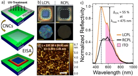
RESULTS AND DISCUSSIONPristine CNC Film Preparation and Optical Character-ization. The CNCs were obtained by chemically breaking down (sulfuric acid hydrolysis) microcrystalline cellulose into high aspect ratio nanorods, which remain stabilized in aqueous suspension due to sulfate groups on the CNCs’ surface.22,23A CNC suspension with 3 wt % and pH of 3 was used forfilm preparation.Figure 1a shows a schematicflow diagram of the technique used to achieve the square shaped photonicfilms. A poly(ethylene naphthalate) (PEN) mask, with a 1 cm× 1 cm opening, was used as a shadow mask during UV irradiation to define a hydrophilic area on the otherwise hydrophobic indium−tin-oxide (ITO) film, which functions as a reservoir
for 100 μL of CNC suspension. After EISA in a controlled environment (T = 23 °C and 25% relative humidity (RH)) until constant weight, iridescent square films are obtained, which selectively reflect LCPL and transmit RCPL as confirmed macro- and microscopically inFigure 1b. The area inside the dashed line marks the region of thefilm with highest uniformity, not only in thickness (around 10μm) and surface roughness but also in photonic response. These properties are strongly affected by the coffee ring effect when moving to the outer parts. POM images taken from the indicated area show a typical monodomain mosaic structure, evidencing a predom-inant blue coloration. Taken from the same area, Figure 1c shows the normalized reflectivity as a function of the visible light spectrum for LCPL (orange line) and for RCPL (black line). Because of the internal left-handed twisted structure, the films show a clear distinction between LCPL and RCPL (ΔCPL
≈ 55%). The reflected wavelength (λreflected) is calculated by
the de Vries equation24
λreflected =n P sinavg θi (1) where navg is the average refractive index of the medium, P
denotes the distance of a full nematic director rotation (see the Supporting Information S1), and θi represents the angle
between the incident light and the chiral nematic layers. The maximum reflected wavelength (λmax= 475 nm) fromFigure
1c results from the contribution of the average of coinciding pitch values in the measured area.25
Figure 1d shows a size distribution study of individual CNC rods on a mica surface by atomic force microscopy (AFM). It is possible to observe elongated ricelike nanorods with high aspect ratios of around L/d = 41. Additional surface topography measurements show that thefilms (seen inFigure 1b) obtained from these CNCs are characterized by a very low surface roughness due to excellent packing of the nanocrystals, yielding on average 36.5 nm rms, which is well below the surface roughness reported for conventional office paper (≈6.4 μm rms).26
Consequently, the obtained droplets of pristine CNC present photonic properties in the visible light spectrum and a very smooth surface for thin or thick film deposition. However, it was found that these droplets lack the necessary Figure 1.Film preparation and characterization. (a) Schematicflow diagram of the CNC deposition process. (b) Macro (taken by a camera) and micro (obtained by polarized optical microscopy (POM)) images of the photonic droplets under CPL illumination. Scale bars indicate 2 mm and 100 μm, respectively. (c) Distinct photonic response in normalized reflectivity as a function of the wavelength. The pink area indicates an underlying contribution to the reflectivity coming from the ITO thin film. (d) CNC lengths (L) and widths (d) as measured by atomic force microscopy (AFM). Scale bar indicates 500 nm.
electrolytic performance to induce conducting channels into semiconductors at low voltages through electric double layer (EDL) charging, when used as dielectrics in transistors. Therefore, an ionic infiltration procedure was adopted to enrich the pristine photonic films (from here on treated as CNC:0) with distinct alkali ions while maintaining their photonic character (from here on treated as CNC:Li, CNC:Na, and CNC:K, for the respective ions, or in general CNC:M). Another advantage of using chiral nematic films instead of their isotropic counterparts, where no nanoscale ordering or photonic bandgaps are observed, is the fact that ionic doping through infiltration (as described in the next section) is facilitated due to their mesoporous structure, arising from the EISA process. The self-assembly gives rise to micro-and nanopores, whereas isotropic CNC suspensions originate a more tightly packed matrix. Ionic infiltration is therefore more homogeneous into the porous chiral nematic network where ions diffuse with more facility. This can be observed in the Supporting Information S2, where cross-sectional EDS confirms this hypothesis for a potassium infiltration into an isotropic and a chiral nematic CNCfilm.
Ionic Doping of Photonic Films. To obtain the ion-enriched photonic electrolytes, thefilms were submersed 1 h in 10 mL of 0.5 M lithium, sodium, or potassium hydroxide solutions, depending on the desired ion and afterward dried under nitrogen flux until constant weight. Figure 2a shows photographs under LCPL illumination of the three infiltration stages: initial state, submersed, and final state after drying. During ion infiltration a visible red-shift is observed, indicating an increase of the pitch through swelling and refractive index matching, affecting P and navg of eq 1, increasing λreflected.
Interestingly, the red-shift decreases when moving from LiOH to KOH. This trend can be explained by the increase in
hydration shell and number when moving from Li+ to K+, which results in a higher amount of infiltrated water (Li > Na > K), increasing swelling and pitch.27 Visually, the final and initial states are identical, which shows that chiral nematic ordering is preserved inside the films. This is confirmed by POM imaging (see Figure S3a) and reflectance spectroscopy where Figure 2b plots ΔCPL and λmax against the films after
infiltration. On average, the films show similar behavior, not diverging beyond each other’s standard deviations with ΔCPL
laying on average between 55% and 60% andλmaxbetween 450
and 500 nm. The films are also suited for application in transparent electronics (seeFigure S3b) as they show a high transmittance of around 80% outside their photonic bandgap (forλ ≥ 450 nm seeFigure S3c).
The use of paper, or cellulose for that matter, as an electrolyte can be attributed to its inherent ability of water retention (either adsorbed or coordinated), which forms a three-dimensional network, aiding in the process of ionic conduction. Consequently, for a solid-state electrolyte with a fixed ionic concentration we would expect higher ionic conductivity when increasing the amount of water in its structure, resulting in enhanced properties for the envisioned application as a solid-state electrolyte in EGTs. Figure 2c shows the Fourier transform infrared spectroscopy (FTIR) spectra of thefilms, which help to trace the amount of water that is retained by thefilms. From the inset ofFigure 2c we can observe the typical absorption bands of cellulose, such as H-bond stretching of OH groups between 3600 and 3000 cm−1, C−H stretching at 2900 cm−1, or the characteristic cellulose bands between 1800 and 600 cm−1.28Additionally, two specific bands for water retention can be identified. These are connected to OH bending of the adsorbed water molecules (1635 cm−1) and their interaction with the OH groups of the Figure 2.Ion infiltration of chiral nematic droplets, and optical characterization. (a) Flow diagram of the adopted ion infiltration process visualized through LCPL light. Scale bars represent 5 mm. (b) Comparison of CPL response (ΔCPL) and photonic bandgap wavelength (λmax) for CNC:0 and
infiltrated films. Error bars shown are standard deviations of five independent measurements. (c) FTIR curves of pristine and infiltrated films.
cellulose chains (3600−3000 cm−1).29
The spectra can be normalized to the C−H stretching band at 2900 cm−1which forms a common baseline for the study of water content inside the films. We observe that the infiltrated films show higher water content when compared to CNC:0. The addition of species with considerable hydration enthalpies into the mesoporousfilms increases their hygroscopic behavior, which results in an increase of adsorbed water species. At the 1635 cm−1 band we observe that the trend of total amount of adsorbed water follows the hydration energies of the ions (Li > Na > K). This trend is also traceable during electrochemical characterization below, where CNC:Li shows the highest ionic conductivity.
X-ray Photoelectron Spectroscopy (XPS). XPS survey spectra (seeFigure S4.1) were run for each sample. Detailed spectra of carbon (C 1s), oxygen (O 1s), sulfur (S 1s), and the individual alkali metals (Li 1s, Na 1s, and K 2p) were recorded and used for proof of ionic doping and respective atomic quantification.Figure 3a depicts the deconvoluted O 1s, C 1s, and S 2p and alkali metal core level spectra of the surface. A similar set of spectra taken from the CNC:M/ITO interface can be found inFigure S4.2.
In Figure 3a clear differences in chemical activity are observed when comparing KOH to NaOH and LiOH treatments. Whereas the O 1s and C 1s peaks of CNC:K are basically identical to the CNC:0 ones, we see pronounced peak
changes for CNC:Li and CNC:Na. This indicates increased reactivity of the LiOH and NaOH species with both the cellulose and the sulfate groups, which shall be discussed in more detail in the following.
The O 1s emission before infiltration can be fitted with only one component, which is assigned to the CNC structure (OCNC). After ion infiltration, a second component arises at lower binding energies (OM). The ratio of the OMto the OCNC component directly reflects the atomic concentration of infiltrated ions, being highest for sodium, intermediate for lithium, and lowest for potassium. Additionally, the binding energy of OMdecreases with decreasing electronegativity of the
respective alkali metal. These two observations confirm that the OMcomponent corresponds to oxygen bonded to the alkali metal ions.
For the C 1s emission we obtained four peaks after deconvolution, corresponding to carbon with no oxygen bond (C1), carbon with a single oxygen bond (C2: corresponding mostly to ether groups and C−O), carbon with two oxygen bonds (C3: corresponding to carbonyl and anomeric carbons in cellulose), andfinally a high binding energy component for carbon with three oxygen bonds with a relative area below 2% (C4: for carboxyl or ester groups, not expected for this type of cellulose).30,31 The C 1s emissions indicate changes to the carbon bonds of the cellulose backbone which showed to be more pronounced with increased alkali ion reactivity, as has Figure 3.X-ray photoelectron spectroscopy and atomic quantification. (a) Core level spectra of O 1s, C 1s, S 2p, and alkali metals and the respective deconvoluted peaks. (b) Atomic concentration of sulfur (blue curves) and alkali metal ions (red curves) on the surface (solid line) and at the CNC:M/ITO interface (dashed line).
been reported for similar treatments of cellulose with alkaline solutions. The most pronounced decrease in oxygenated carbon species is observed for the CNC:Li and CNC:Na films compared to CNC:0 and CNC:K, the latter two being practically the same in this respect.
Furthermore, the S 2p binding energies confirm the presence of the sulfate groups that form on the surface of the CNCs during the hydrolysis with sulfuric acid.32 Moreover, the individual alkali emissions prove the success of the ionic doping process.33 The next important observation is the correlation between the amount of infiltrated ions and the sulfur content, represented in Figure 3b. It is known that NaOH is a strong candidate for desulfonation reactions on sulfuric acid-treated CNCs.32,34 A possible reaction during desulfonation is the replacement of the sulfate groups by either −OH or −ONa, the latter being confirmed by the intensity changes and the chemical shifts of the OM component, as described above. This modification to the CNCs not only results in a loss of anisotropy when in suspension but also decreases the S 2p peak intensity of suspensions and dryfilms. Consequently, and as observed in Figure 3b, for NaOH infiltration we trace such a desulfonation reaction. Notably, no bond changes for S 2p can be inferred as only a change in intensity but not in binding energy is measured. This confirms that the sulfate groups are simply washed out after
desulfonation. We see that LiOH has a similar effect with a decrease in sulfur concentration. However, it is noted that these reactions only occur partially, as the S 2p peaks do not disappear completely. With the occurrence of desulfonation we also see higher Li+and Na+concentrations (Figure 3b). On the
other hand, no significant desulfonation occurs for KOH, indicating a relatively low reactivity with the CNCs. Furthermore, when we compare the top surface concentrations with the ones at the CNC:M/ITO interface in Figure 3b (dashed line), a visible decrease in ionic concentration for Li+ and Na+ is observed (Li+ and Na+ atomic concentrations decrease throughout thefilm from 5% and 9.2% to 1.3% and 2%, respectively). As these ions react more strongly with the CNCs, they are not efficient for uniform infiltration. Potassium, on the other hand, is the only one that infiltrates thefilms homogeneously from top to bottom with an atomic concentration of around 1%.
Electrochemical Characterization. To assess electro-chemical behavior, electrolytic capacitors with the CNCfilms as solid-state electrolytes were fabricated as depicted inFigure 4a and investigated through electrochemical impedance spectroscopy (EIS), cyclic voltammetry (CV), and chronoam-perometry.
It was possible tofit the data by using the equivalent circuit model (ECM) depicted inFigure 4b, containing a double time Figure 4.Electrochemical impedance spectroscopy. (a) Electrochemical cell structure with a colored cross-section SEM image of a CNC:Mfilm, showing monodomains, distinct pitch values, and mesoporous structure. Arrows indicate the micropores described by the equivalent circuit model (ECM). Scale bar = 400 nm. Identification of the ECM elements (1, 2, and 3). (b) ECM used for data fitting (WE = working electrode and CE/RE = counter and reference electrodes). (c) Phase as a function of applied frequency and respectivefittings. (d) Nyquist plot of the obtained data and respectivefittings. Inset shows zoom of indicated area.
constant (two RC components), accounting for the porous character of the chiral nematic films. This ECM has been successfully used to fit coatings with pocket or pore formations.35 In the case these pockets or pores are filled with electrolyte they will contribute to the electrochemical behavior of the cell under study as additional solid/electrolyte interfaces are created, where EDLs form.36In our case we can imagine that through the chiral nematic character the resulting anisotropy gives rise to nanopores because of the repulsive forces between individual CNCs. Further investigations report on grooves and gaps even in the micrometer range, which are formed during the drying process.23,37Figure 4a also shows a cross-section SEM image of a CNCfilm. During drying initial tactoid formations at the gel state give rise to monodomains with distinct pitch values (indicated as pitch 1, 2, and 3). During the process these monodomains contract like springs that were left under extension, leaving behind pores in the micrometer range (yellow arrows in Figure 4a). These observations led us to the proposed ECM to describe the electrochemical data obtained during EIS. Comparing numeration from Figure 4a,b, the model is composed of an impedance Rc(1), taking into account the contact resistance of
the used electrodes, a RC circuit (2) describing jointly the resistance of the film (Rf) and interface double-layer
capacitance (Cdl), and finally a second RC circuit (3)
accounting for the mesopores and nanogaps throughout the CNCfilm with pore resistance and capacitance (Rpoand Cpo,
respectively).Figures 4c and4d show the resulting phase and Nyquist plots from EIS, where the used ECM describes the obtained data in both the high- and low-frequency regimes, accounting for dipolar and ionic relaxation modes, respectively.
The films show a capacitive regime between 10 Hz (for CNC:Li) and 1 Hz (for CNC:0). This gives already a hint about an increased ionic conductivity for CNC:Li when compared to CNC:Na, CNC:K, and CNC:0. This assumption however can be better analyzed by the Nyquist plots inFigure 4d, where thefilms show a compressed semicircle, indicating inhomogeneous charge distribution across the EDL at the CNC/electrode interfaces. This leads to the use of constant phase elements (CPE) as nonideal capacitors in the ECM. Qualitatively, we can identify a difference between the CNC:0 film and the infiltrated ones. The semicircles shorten through the addition of ions and water retention into thefilm, reflecting an increase in ionic conductivity.38 An increase in retained water promotes a higher chance of its dissociation to give OH− and H+that can migrate through the structure, as proposed by
other works.39−41 The increased amount of water thus increases not only ionic conductivity but also EDL formation leading to higher double-layer capacitances, as will be seen by CV measurements below. The inset ofFigure 4d zooms in on the marked area and reveals the individual semicircles of the infiltrated films. In Nyquist plots the width of the semicircle (indicated as Rf) characterizes the bulk resistance, which can
be extracted to yield the ionic conductivity (σi). The plots indicate that a decrease in ionic radius of the infiltrated cation leads to decreased Rfand thus an increase in ionic conductivity (Li+ > Na+ > K+). This shows again accordance with the increased water content observed via FTIR.
Double-layer capacitance (CDL) was measured by using CV
and considering a linear increase of the charging current (IC) with the scan rate (dv(t)/dt) at low voltages followingeq 2:
= − = I I I C v t t 2 d ( ) d C a b DL (2)
Figure 5.Cyclic voltammetry (CV) and chronoamperometry. (a) CV of thefilms with ±100 mV around open circuit potential (VOC) at different
scan rates. (b) Ionic conductivity and double-layer capacitance (CDL) as a function of samples. The orange box indicates capacitances usually
achieved for conventional office paper (around 100 nF cm−2).42(c) Chronoamperometry with an excitation potential of Vexc= 50 mV at 5 s. The
inset shows the peak capacitive current reached at excitation. (d) Capacitance retention over 4000 cycles. (e) CV for electrochemical cell with a-IGZO at the working electrode as indicated by the inset to measure faradaic and capacitive currents.
where Iaand Ibare the maximum and minimum currents at the
open circuit potential (VOC) for a specific CV curve. The CV
curves represented inFigure 5a show higher currents for the infiltrated films when compared to CNC:0, approaching also more ideal capacitor characteristics (more rectangular curve shape).
Figure 5b summarizes ionic conductivity and CDLobtained through EIS and CV, respectively (taking CNCfilm thickness ≈10 μm and electrode dimensions (1 mm × 1 mm) into account). We observe that both parameters are greatly enhanced through ionic doping, seeing an increase of 1 order of magnitude. For the ion-enriched films, we see a continuous decrease when moving from CNC:Li to CNC:K, which is again connected to the individual hydration enthalpy and the ability for water retention and its dissociation. The same trend was observed during chronoamperometry (Figure 5c) where an excitation potential of Vexc= 50 mV was applied to observe the exponential CDLdischarge over time. The inset
depicts the achieved peak currents ICpeakat excitation, and we observe again a decrease when moving from CNC:Li to CNC:K, which is directly related to the CDLof thefilms. The films were also cycled up to 4000 times (Figure 5d), evidencing excellent CDL retention. Interestingly, the ion-enrichedfilms seem to need some cycles to fully stabilize their capacitance which can be connected to charge redistribution inside the films from a pristine state during initial cycling. A property that was not observed for the CNC:0 films, as no infiltrated ions are present for redistribution.
In summary, our findings show that in an ideal electrolytic capacitor lithium is indeed a better ionic conductor for this type of solid-state electrolyte, as higher ionic conductivities and capacitances were consistently achieved with CNC:Li. These results show potential use in electrolytic capacitors or applications with ideally polarizable cells. However, the interest herein lays in their potential use in electric double-layer transistors (EDLTs), and thus electrochemistry at the electrolyte/semiconductor interface plays an important role. For pure EDL charging (desirable in EDLTs), capacitive charging should be maximized and faradaic currents, which are connected to mass transfer across the interface (desirable for electrochemical transistors, ECTs), should be minimized. To study the interaction between our photonic electrolytes and the employed semiconductor, a-IGZO was deposited between the CNC:M films and the working electrode as depicted in Figure 5e. CV curves for these test structures were run (depicted inFigure 5e) at identical gate potentials (between −0.5 and 2.0 V) and scan rates (500 mV s−1) used to turn the
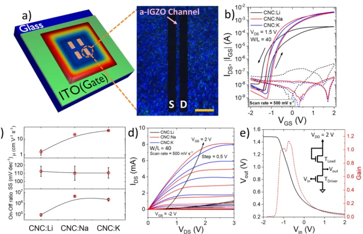
transistors to the on-state. From the curves we observe that considerable faradaic currents arise for CNC:Lifilms of up to 1 order of magnitude higher than for CNC:Na and CNC:K films. This indicates that a-IGZO is permeable to Li ions that diffuse into the semiconductor across the electrolyte/semi-conductor interface, which can be detrimental for transistor performance (see the Supporting Information S5). The electrochemical results are confirmed during transistor characterization below, where improved transistor parameters Figure 6.Transistor and inverter characterization. (a) Schematic device architecture with microscope image of a single transistor in reflection mode with LCPLfilter. Scale bar indicates 500 μm. (b) Transfer curves where IDSand IGSare represented by solid and dashed lines, respectively. (c)
Comparison of saturation mobility (μ) subthreshold swing (SS) and on/off ratios. All error bars shown are standard deviations of at least five different devices. (d) Output curves for a VDSsweep from 0 to 3 V and distinct VGSreaching from−2 to 2 V in 0.5 V steps. (e) Voltage transfer
curve of an inverter on CNC:Na with diode connected load. The inset shows a schematic of the circuit.
advantages when compared to planar types (where S/D and gate (G) lay in the same plane), namely, faster ionic movement due to a more uniform electric field distribution in the dielectric, leading to faster switching and lower operation voltages.44 The inset shows an amplification of a single transistor on top of a CNC:Na film. Here, the underlying photonic character becomes evident.
Figure 6b plots the drain and gate currents (IDS and IGS,
respectively) as a function of applied gate voltage (VGS) at S/D
voltage (VDS) of 1.5 V. The devices work at very low voltages
with high on−off ratios (Ion/Ioff≈ 6 orders of magnitude) and present a counter clockwise behavior with low hysteresis. The obtained results show the potential of the ionic doping of CNC films, as transistors on pristine CNC films showed very low current modulation for high VDS and VGS (Supporting Information S6). A negative turn-on voltage (Von) of about
−1 V is observed, conferring a depletion mode behavior. Observations made during EIS hold also true during transistor characterization. Despite CNC:Li showing highest ionic conductivity and CDL, Li+ions tend to diffuse into the
a-IGZO, which results in a collapse of the interface EDL and therefore charge accumulation in the channel of the transistor (observe inFigure 6b an increase in leakage current (IGS) and a
decrease in on current for CNC:Li). IGS is higher because of
the faradaic redox currents that were also observed during CV. On the other hand, increased capacitive charging for CNC:Na and CNC:K lowers IGS and greatly enhances transistor characteristics. Figure 6c plots the transistor parameters for the different CNC films, showing an increased channel mobility (μ) and on/off ratio when moving from Li+ to K+
(for data and equations see theSupporting Information S7), despite the curves of CNC:Na and CNC:K being almost identical. However, even with CNC:K having lowest CDL the
reached channel mobility is higher than for transistors on CNC:Na (seeFigure 6c). An explanation is that Na+might be more strongly bound at the CO− groups after desulfonation than K+, as discussed in theXPS section. This ultimately could
play a role in the ionic polarizability, and consequently the CNC:K films show higher mobility. Also, a more uniform infiltration throughout the film was confirmed by XPS which clearly improves the performance of CNC:K films as an electrolyte in these devices. It is important to note that the mobility calculated here (especially for CNC:K = 35.86 cm2 V−1 s−1) is quite high when compared to similar transistors employing IGZO in either electrolyte gated or conventional oxide dielectric transistors.45−48We have to be aware in this situation that this exceptionally high mobility might be due to
DS
An NMOS inverter circuit composed of two identical transistors on CNC:Na with a diode-connected load was fabricated as depicted schematically in the inset ofFigure 6e. The voltage transfer curve shows a clear inverting behavior with a logic swing around 1.25 V and unity gain, since the load and driver transistors have the same characteristics. If additional amplification is intended, either transistor sizing needs to be changed, to obtain disparities in transconductance between the two, or the load transistor needs to be replaced with a fixed resistance load. The inverter and transistors presented here are expected to work beyond the frequency where the ion-doped CNC films present a predominant capacitive regime, since the maximum on current remains in the range of hundreds of microamperes at 10 Hz, resulting in on/off current ratios still above 105 (see the Supporting
Information S8).
■
CONCLUSIONIn summary, we report on the integration of ion infiltrated twisted mesoporous photonic dried droplets based on cellulose nanocrystals (CNCs) into semiconductor devices and inverter circuits. The presented ionic doping technique infiltrates alkali metal ions into CNCfilms after they went through evaporation induced self-assembly and attained their final chiral nematic arrangement. This way the CNCs are locked in space and maintain anisotropy and thus specific photonic bandgaps. Distinct circular polarized light (CPL) reflection (up to 60% distinction between left- and right-handed CPL) in the visible region (475 nm) was measured through polarized optical microscopy. XPS evidences the presence of alkali metals in the CNCfilms after infiltration and shows significant changes to C 1s, O 1s, and S 2p peaks for lithium and sodium infiltrated films, whereas potassium infiltrated films remain like the pristine ones. Desulfonation and changes to the carbon bonds of the cellulose backbone are registered for LiOH and NaOH treatment, whereas KOH does not affect the CNCs as much. Nevertheless, XPS confirms the ionic doping with atomic concentrations of 5%, 9%, and 1% for Li+, Na+, and K+,
respectively. Electrochemical characterization shows a consid-erable increase in capacitance and ionic conductivity when comparing the infiltrated with the pristine films. CNC:Li films show the highest CDLand ionic conductivity. However, when in contact with a-IGZO, Li ions start to diffuse into the semiconductor, giving rise to faradaic currents. Pure capacitive charging (favorable for electric double-layer transistor implementation) was observed for CNC:Na and CNC:K films. This observation is confirmed during transistor
characterization, where devices on CNC:Na and CNC:K showed better performances. The devices work in depletion mode (VOn < 0 V) with on−off ratios up to 6 orders of
magnitude and saturation mobilities of up to 35 cm2V−1s−1,
which might, however, be conditioned by an underestimated CDL. Additionally, steep subthreshold swings of 100 mV dec−1 were achieved conferring fast on−off transitions. An inverter circuit was implemented to show the potential use in logic microelectronic circuitry. As future perspectives it would be interesting to applyfirst-principles calculations, taking kinetic and thermodynamic parameters into account, to model the double-layer and electronic structure at the electrolyte/ semiconductor interface.49
The results are intriguing as previous works concentrated mostly on the smallest possible ions (Li+) with highest ionic
conductivity for their use in electrolyte gated transistors. Especially for paper gated transistors, this work might give a push into the direction of more abundant ionic conductors such as sodium or potassium, which were not expected to yield improved electrochemical characteristics in combination with nanocellulose and the employed amorphous IGZO as semiconductor. The types of cellulose-based solid-state electrolytes presented here with directional anisotropy and photonic bandgaps mightfind use in a vast field of applications ranging from batteries to supercapacitors and optoelectronic devices for light or electrochemical sensing or even in the printing technology area.
■
METHODSCNC Preparation. CNCs were obtained as described elsewhere.10
The CNC suspension with a 3.00 ± 0.05% w/w (gravimetrically determined) was used in its acid form (pH = 3). Nanoparticles with 137.30± 39.81 and 3.33 ± 1.01 nm of length and width, respectively, and an aspect ratio 41.23± 17.30 were obtained (determined from 50 measures with ImageJ, version 1.45 s, of the nanoparticles observed by AFM). These particle dimensions are in accordance with the ones described in the literature for similar hydrolysis times.50
CNC Film and Infiltration. To produce the pristine CNC films from suspension a hydrophobic ITO surface on glass was irradiated with UV for 20 min (PSD Series, Digital UV Ozone System by NOVASCAN). A rectangular mask with an opening of 1 cm was used, which left the central area exposed to the treatment, while the rest of the substrate remained protected and hydrophobic. Post-UV exposure the CNC suspension only spread inside the treated area, which gave rise to rectangularfilms. The films were left for 24 h to dry in a controlled environment (SICCO, 25% RH, T = 21 °C). Ion infiltration was performed in a round polystyrene Petri dish with a diameter of 3 cm. The used solutions for infiltrations were 10 mL of 0.5 M hydroxide solution (LiOH, NaOH, or KOH). The glass/ITO substrates with thefilms were placed in the solution facing up and left for infiltration for 1 h, after which the samples were removed and rinsed off in ultrapure water for 3 s for washing, followed by nitrogen drying.
Profile and AFM. Thickness measurements were performed using a XP-200 profilometer from AMBIOS Technology. Surface scanning was performed with a speed of 0.1 mm s−1and a stylus force of 1 mg. Atomic force microscopy was performed on an Asylum Research MFP-3D Stand Alone system operated in alternate contact mode. Commercially available silicon AFM probes (Olympus AC160TS; f0
= 300, k = 26.1 N m−1) were used to generate the surface images, which were then plane-fitted.
Optical Characterization (Macroimaging, POM, and FTIR). Macroimages were taken in reflectance mode by a LEICA IC80 HD camera with a LEICA magnifying lens. An Edmund Optics plastic circular polarizer (with T > 40% forλ between 400 and 800 nm) was used for LCPL and RCPL images. POM images were obtained in
reflection mode by using an Olympus BX51 microscope, coupled with an Olympus DP73 CCD camera, and acquired with the Stream Basic v.1.9 Olympus software. A cold illumination source generated by a halogen lamp (KL 2500 LCD, Olympus) was used. The images were obtained with×10 objectives (Olympus, MPlanFL N). To detect the reflection of right- and left-handed circularly polarized light, a quarter-wave plate (U-TP137, Olympus) coupled with a polarizer was inserted in the optical path. The reflective wavelengths detected for LCPL and RCPL channels were recorded with a Jobin Yvon monochromator H10 Vis, equipped with a photomultiplier mounted onto the microscope, and acquired with the Jobin Yvon Autoscan v 1.22 software. Fourier-transform infrared (FTIR) spectroscopy acquisitions were performed at room temperature by using an attenuated total reflectance (ATR) sampling accessory (Smart iTR) equipped with a single-bounce diamond crystal on a Thermo Nicolet 6700 spectrometer, with the following conditions: incident angle of 45°, 4000−650 cm−1range, 4 cm−1resolution, and 32 scans.
X-ray Photoelectron Spectroscopy (XPS). An Axis Supra spectrometer by Kratos Analytical was used with monochromatic Al Kα radiation. Because of the insulating character of the samples, charge neutralization with an electron flood gun and charge referencing of the C1 component to 284.8 eV were employed. The top surfaces were analyzed with a pass energy of 5 eV, giving rise to an energy resolution better than 0.45 eV. For the interface surfaces, an aperture of 55μm and a pass energy of 80 eV were used. Detaching the CNCfilms from the substrates was achieved by peeling off using double-sided carbon tape attached to the top surface.
Electrochemical Characterization. Electrochemical character-ization was performed using a Gamry Instruments Reference 600 potentiostat at room temperature (23± 2 °C, ≈40% RH) in a typical capacitor structure with evaporated gold contacts with an active area of 1 mm2 and ITO as the bottom electrode. For electrochemical
impedance spectroscopy, measurements were performed with a 10 mV ac signal in a frequency range between 0.1 and 106Hz. Cyclic
voltammetry was performed at different scan rates (50, 100, 250, and 500 mV s−1) and±100 mV around open-circuit potential (VOC). The
stability was evaluated with CV over 4000 cycles at a frequency of 500 mV s−1. For CV with the semiconductor,first a-IGZO was deposited at the working electrode and on top gold contacts. CV was performed between −0.5 and 2 V at a fixed scan rate of 500 mV s−1. Chronoamperometry was performed with an excitation potential of Vexc= 50 mV, and the charging current was recorded for 100 s.
Transistor Fabrication and Characterization. The transistors were fabricated at room temperature without any substrate heating or postprocess annealing. The ITO-coated glass substrate served as the common bottom gate electrode (Xin Yan Technology Limited, XY15s, 15Ω sq−1, polished with T > 85% at 550 nm and thickness of 155 ± 20 nm). The CNC films served as gate dielectric with the sputtered amorphous indium−gallium−zinc−oxide (a-IGZO: In2O3−
Ga2O3−ZnO; 2:1:2 mol % using an AJA ORION system) as the
active oxide semiconductor on top, followed by titanium/gold (Ti/ Au−electron beam evaporated 6 and 65 nm, respectively) source and drain contacts. Everything was patterned by using shadow masks with a channel width (W) of 2000μm and length (L) of 50 μm (W/L = 40). Electrical characterization of the devices was performed at room temperature by using a Keithley 4200-SCS and a JANIS ST-500 probe station. Transfer curves were conducted with a VGSsweep of 0.1 V
steps from−2 to 2 V with VDS= 1.5 V. Time interval between VGS
points was 0.1 s. Output curves were run with VDSranging from 0 to 3
V in 0.1 V steps with VGSbetween−2 and 2 V in 0.5 V steps.
■
ASSOCIATED CONTENT*
S Supporting InformationThe Supporting Information is available free of charge at https://pubs.acs.org/doi/10.1021/acsaelm.9b00652.
S1: SEM cross-section image of a CNC film with indication of nematic director rotation; S2: ionic infiltration into isotropic and anisotropic (chiral
Notes
The authors declare no competingfinancial interest.
■
ACKNOWLEDGMENTSP.G. acknowledges the support from FCT − Portuguese Foundation for Science and Technology through the Ph.D. scholarship SFRH/BD/125191/2016. The authors acknowl-edge the European Commission under project NewFun (ERC-StG-2014, GA 640598) and BET-EU (H2020-TWINN-2015, GA 692373). This work was also supported by the FEDER funds through the COMPETE 2020 Program and the National Funds through the FCT− Portuguese Foundation for Science and Technology under Project POCI-01-0145-FEDER-007688, Reference UID/CTM/50025, project PapEl, ence PTDC/CTM-NAN/5172/2014, project CHIHC, refer-ence PTDC/NAN-MAT/32558/2017, project PTDC/CTM-BIO/6178/2014, M-ERA-NET2/0007/2016 (CellColor), and POR Lisboa2020 through project PTDC/CTM-REF/30529/ 2017. D.G. acknowledges the support from FCT− Portuguese Foundation for Science and Technology through the AdvaMTech PhD program scholarship PD/BD/52627/2014. J.D. acknowledges funding received from the European Union’s Horizon 2020 research and innovation program through the project HERACLES (Project No. 700395).
■
REFERENCES(1) Ha, D.; Fang, Z.; Zhitenev, N. B. Paper in Electronic and Optoelectronic Devices. Adv. Electron. Mater. 2018, 4 (5), 1700593.
(2) Gaspar, D.; Martins, J.; Bahubalindruni, P.; Pereira, L.; Fortunato, E.; Martins, R. Planar Dual-Gate Paper/Oxide Field Effect Transistors as Universal Logic Gates. Adv. Electron. Mater. 2018, 4 (12), 1870059.
(3) Hon, D. N.-S. Cellulose: A Random Walk along Its Historical Path. Cellulose 1994, 1 (1), 1−25.
(4) Tobjörk, D.; Österbacka, R. Paper Electronics. Adv. Mater. 2011, 23 (17), 1935−1961.
(5) Siegel, A. C.; Phillips, S. T.; Dickey, M. D.; Lu, N.; Suo, Z.; Whitesides, G. M. Foldable Printed Circuit Boards on Paper Substrates. Adv. Funct. Mater. 2010, 20 (1), 28−35.
(6) Celano, U.; Nagashima, K.; Koga, H.; Nogi, M.; Zhuge, F.; Meng, G.; He, Y.; De Boeck, J.; Jurczak, M.; Vandervorst, W.; Yanagida, T. All-Nanocellulose Nonvolatile Resistive Memory. NPG Asia Mater. 2016, 8, e310.
(7) Wu, J.; Lin, L. Y. Ultrathin (<1Μm) Substrate-Free Flexible Photodetector on Quantum Dot-Nanocellulose Paper. Sci. Rep. 2017, 7, 43898.
(8) Gao, L.; Chao, L.; Hou, M.; Liang, J.; Chen, Y.; Yu, H.-D.; Huang, W. Flexible, Transparent Nanocellulose Paper-Based Perov-skite Solar Cells. Npj Flex. Electron. 2019, 3 (1), 4.
(4686), 632−633.
(14) Lagerwall, J.; Schütz, C.; Salajkova, M.; Noh, J.; Park, J. H.; Scalia, G.; Bergström, L. Cellulose Nanocrystal-Based Materials: From Liquid Crystal Self-Assembly and Glass Formation to Multifunctional Thin Films. NPG Asia Mater. 2014, 6 (1), e80.
(15) Wilts, B. D.; Dumanli, A. G.; Middleton, R.; Vukusic, P.; Vignolini, S. Invited Article: Chiral Optics of Helicoidal Cellulose Nanocrystal Films. APL Photonics 2017, 2 (4), 040801.
(16) Tadepalli, S.; Slocik, J. M.; Gupta, M. K.; Naik, R. R.; Singamaneni, S. Bio-Optics and Bio-Inspired Optical Materials. Chem. Rev. 2017, 117 (20), 12705−12763.
(17) Grey, P.; Fernandes, S. N.; Gaspar, D.; Fortunato, E.; Martins, R.; Godinho, M. H.; Pereira, L. Field-Effect Transistors on Photonic Cellulose Nanocrystal Solid Electrolyte for Circular Polarized Light Sensing. Adv. Funct. Mater. 2019, 29, 1805279.
(18) Gray, D. Recent Advances in Chiral Nematic Structure and Iridescent Color of Cellulose Nanocrystal Films. Nanomaterials 2016, 6 (11), 213.
(19) Parker, R. M.; Frka-Petesic, B.; Guidetti, G.; Kamita, G.; Consani, G.; Abell, C.; Vignolini, S. Hierarchical Self-Assembly of Cellulose Nanocrystals in a Confined Geometry. ACS Nano 2016, 10 (9), 8443−8449.
(20) Dong, X. M.; Gray, D. G. Effect of Counterions on Ordered Phase Formation in Suspensions of Charged Rodlike Cellulose Crystallites. Langmuir 1997, 13 (8), 2404−2409.
(21) Dong, X. M.; Kimura, T.; Revol, J.-F.; Gray, D. G. Effects of Ionic Strength on the Isotropic-Chiral Nematic Phase Transition of Suspensions of Cellulose Crystallites. Langmuir 1996, 12 (8), 2076− 2082.
(22) Cranston, E. D.; Gray, D. G. Morphological and Optical Characterization of Polyelectrolyte Multilayers Incorporating Nano-crystalline Cellulose. Biomacromolecules 2006, 7 (9), 2522−2530.
(23) Fernandes, S. N.; Almeida, P. L.; Monge, N.; Aguirre, L. E.; Reis, D.; de Oliveira, C. L. P.; Neto, A. M. F.; Pieranski, P.; Godinho, M. H. MindtheMicrogap in Iridescent Cellulose Nanocrystal Films. Adv. Mater. 2017, 29 (2), 1603560.
(24) de Vries, H. Rotatory Power and Other Optical Properties of Certain Liquid Crystals. Acta Crystallogr. 1951, 4, 219.
(25) Dumanli, A. G.; van der Kooij, H. M.; Kamita, G.; Reisner, E.; Baumberg, J. J.; Steiner, U.; Vignolini, S. Digital Color in Cellulose Nanocrystal Films. ACS Appl. Mater. Interfaces 2014, 6 (15), 12302− 12306.
(26) Pereira, L.; Gaspar, D.; Guerin, D.; Delattre, A.; Fortunato, E.; Martins, R. The Influence of Fibril Composition and Dimension on the Performance of Paper Gated Oxide Transistors. Nanotechnology 2014, 25 (9), 094007.
(27) Mähler, J.; Persson, I. A Study of the Hydration of the Alkali Metal Ions in Aqueous Solution. Inorg. Chem. 2012, 51 (1), 425−438. (28)Łojewska, J.; Miśkowiec, P.; Łojewski, T.; Proniewicz, L. M. Cellulose Oxidative and Hydrolytic Degradation: In Situ FTIR Approach. Polym. Degrad. Stab. 2005, 88 (3), 512−520.
(29) Olsson, A. M.; Salmén, L. The Association of Water to Cellulose and Hemicellulose in Paper Examined by FTIR Spectros-copy. Carbohydr. Res. 2004, 339 (4), 813−818.
(30) Vipin, A. K.; Fugetsu, B.; Sakata, I.; Isogai, A.; Endo, M.; Li, M.; Dresselhaus, M. S. Cellulose Nanofiber Backboned Prussian Blue Nanoparticles as Powerful Adsorbents for the Selective Elimination of Radioactive Cesium. Sci. Rep. 2016, 6, 37009.
(31) Östenson, M.; Järund, H.; Toriz, G.; Gatenholm, P. Determination of Surface Functional Groups in Lignocellulosic Materials by Chemical Derivatization and ESCA Analysis. Cellulose 2006, 13 (2), 157−170.
(32) Lin, N.; Dufresne, A. Surface Chemistry, Morphological Analysis and Properties of Cellulose Nanocrystals with Gradiented Sulfation Degrees. Nanoscale 2014, 6 (10), 5384−5393.
(33) Moulder, J. F.; Chastain, J. Handbook of X-Ray Photoelectron Spectroscopy: A Reference Book of Standard Spectra for Identification and Interpretation of XPS Data; Physical Electronics Division, Perkin-Elmer Corporation: 1992.
(34) Lizundia, E.; Nguyen, T.-D.; Vilas, J. L.; Hamad, W. Y.; MacLachlan, M. J. Chiroptical, Morphological and Conducting Properties of Chiral Nematic Mesoporous Cellulose/Polypyrrole Composite Films. J. Mater. Chem. A 2017, 5 (36), 19184−19194.
(35) Yang, M.; Wu, J.; Fang, D.; Li, B.; Yang, Y. Corrosion Protection of Waterborne Epoxy Coatings Containing Mussel-Inspired Adhesive Polymers Based on Polyaspartamide Derivatives on Carbon Steel. J. Mater. Sci. Technol. 2018, 34, 2464−2471.
(36) GAMRY. Basics of Electrochemical Impedance Spectroscopy. Appl. Note AC 2010, No. 1, 1−17.
(37) Gray, D. G.; Mu, X. Chiral Nematic Structure of Cellulose Nanocrystal Suspensions and Films; Polarized Light and Atomic Force Microscopy. Materials 2015, 8 (11), 7873−7888.
(38) Vélez, J. F.; Procaccini, R. A.; Aparicio, M.; Mosa, J. Epoxy-Silica Hybrid Organic-Inorganic Electrolytes with a High Li-Ion Conductivity. Electrochim. Acta 2013, 110, 200−207.
(39) Yang, J.-T.; Ge, C.; Du, J.-Y.; Huang, H.-Y.; He, M.; Wang, C.; Lu, H.-B.; Yang, G.-Z.; Jin, K.-J. Artificial Synapses Emulated by an Electrolyte-Gated Tungsten-Oxide Transistor. Adv. Mater. 2018, 30 (34), 1801548.
(40) Ge, C.; Liu, C.-X.; Zhou, Q.-L.; Zhang, Q.-H.; Du, Y.; Li, J.-K.; Wang, C.; Gu, L.; Yang, G.-Z.; Jin, K.-J. A Ferrite Synaptic Transistor with Topotactic Transformation. Adv. Mater. 2019, 31 (19), 1900379.
(41) Huang, H.-Y.; Ge, C.; Zhang, Q.-H.; Liu, C.-X.; Du, Y.; Li, J.-K.; Wang, C.; Gu, L.; Yang, G.-Z.; Jin, K.-J. Electrolyte-Gated Synaptic Transistor with Oxygen Ions. Adv. Funct. Mater. 2019, 29 (29), 1902702.
(42) Grey, P.; Gaspar, D.; Cunha, I.; Barras, R.; Carvalho, J. T.; Ribas, J. R.; Fortunato, E.; Martins, R.; Pereira, L. Handwritten Oxide Electronicson Paper. Adv. Mater. Technol. 2017, 2 (6), 1700009.
(43) Dehm, S.; Kruk, R.; Hahn, R.; Stoesser, G.; Dasgupta, S.; Hahn, H.; Schweikert, N. Printed and Electrochemically Gated, High-Mobility, Inorganic Oxide Nanoparticle FETs and Their Suitability for High-Frequency Applications. Adv. Funct. Mater. 2012, 22 (23), 4909−4919.
(44) Grey, P.; Pereira, L.; Pereira, S.; Barquinha, P.; Cunha, I.; Martins, R.; Fortunato, E. Solid State Electrochemical WO 3 Transistors with High Current Modulation. Adv. Electron. Mater. 2016, 2 (9), 1500414.
(45) Kumar, N.; Kumar, J.; Panda, S. Back-Channel Electrolyte-Gated a-IGZO Dual-Gate Thin-Film Transistor for Enhancement of PH Sensitivity Over Nernst Limit. IEEE Electron Device Lett. 2016, 37 (4), 500−503.
(46) Chae, M.-S.; Park, J. H.; Son, H. W.; Hwang, K. S.; Kim, T. G. IGZO-Based Electrolyte-Gated Field-Effect Transistor for in Situ Biological Sensing Platform. Sens. Actuators, B 2018, 262, 876−883.
(47) Park, S.; Lee, S.; Kim, C.-H.; Lee, I.; Lee, W.-J.; Kim, S.; Lee, B.-G.; Jang, J.-H.; Yoon, M.-H. Sub-0.5 V Highly Stable Aqueous Salt Gated Metal Oxide Electronics. Sci. Rep. 2015, 5, 13088.
(48) Nomura, K.; Ohta, H.; Takagi, A.; Kamiya, T.; Hirano, M.; Hosono, H. Room-Temperature Fabrication of Transparent Flexible Thin-Film Transistors Using Amorphous Oxide Semiconductors. Nature 2004, 432, 488.
(49) Han, B.; Viswanathan, V.; Pitsch, H. First-Principles Based Analysis of the Electrocatalytic Activity of the Unreconstructed Pt(100) Surface for Oxygen Reduction Reaction. J. Phys. Chem. C 2012, 116 (10), 6174−6183.
(50) Revol, J.-F.; Godbout, L.; G. Gray, D. Solid Self-Assembled Films of Cellulose with Chiral Nematic Order and Optically Variable Properties. J. Pulp Pap. Sci. 1998, 24, 146−149.