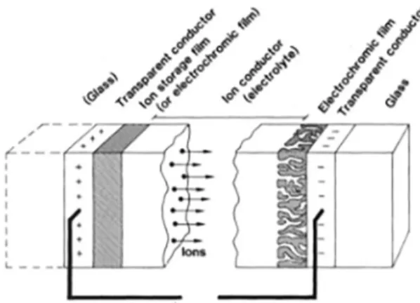
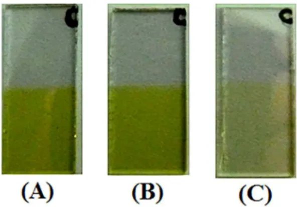
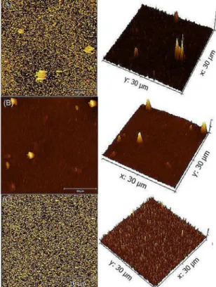
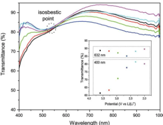
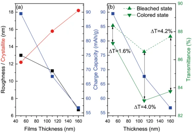
Commitment Between Roughness and Crystallite Size in the Vanadium Oxide Thin Film opto-electrochemical Properties
Texto
Imagem
Documentos relacionados
Representative fluorescent micrographs showing Bone Marrow derived Osteoclast Lineage Cells (BMC) after 3 days of culture and upon 3 hours of incubation with
In this study, the tumors with 5C ploidy lower than 3.15 showed associa- tion with better survival rates when compared to tumors with an elevated percentage of 5C cells, with
incorporation of the TPA group on chalcone structure has been performed and the photophysical and electrochemical properties of TPA-chalcone derivatives have been
Conclui que se trata de um tributo, em especial uma contribuição social, posto que o artigo 4º do Código Tributário Nacional ensina que a destinação é
Then, the LiFePO 4 /PAni composite was synthesized by chemical synthesis and its electrochemical properties as cathode material in lithium ion batteries were
The role played by the firing process in the film preparation and the crystallite size of HA and BTO on the dielectric constant and structural properties of the films are discussed..
➢ Melhorar a capacidade de exaustão do edifício 1 da fábrica com vista a assegurar as condições exigidas de exaustão para cada máquina, assim como preparar o sistema de
Em Jean-Luc Godard, Cinema Historian, Michael Witt procura demonstrar que muitos dos temas, metodologias e preocupa- ções expressas por Godard no projeto das Histoire(s) –
