circular polarized light (LCPL and RCPL, respectively) is reported. The CNC films with a left-handed internal long-range order are infiltrated with sodium ions to yield solid-state electrolytes with photonic properties capable of LCPL reflection and RCPL transmission. They are employed as gate dielectrics in sputtered amorphous indium–gallium–zinc oxide (a-IGZO) transistors. The obtained devices operate in depletion mode at low voltages (<2 V) with On–Off ratios of up to 7 orders of magnitude, subthreshold swings around 80 mV dec−1, and saturation mobilities up to 9 cm2 V−1 s−1. Combining the
photonic character of the CNC films with the light sensitivity of a-IGZO, the devices are capable of discrimination between LCPL and RCPL signals in the blue region. These type of devices can find application in photonics, emis-sion, converemis-sion, or sensing with CPL but also imaging or spintronics.
DOI: 10.1002/adfm.201805279
P. Grey, Dr. S. N. Fernandes, D. Gaspar, Prof. E. Fortunato, Prof. R. Martins, Prof. M. H. Godinho, Prof. L. Pereira CENIMAT/I3N
Departamento de Ciência dos Materiais Faculdade de Ciências e Tecnologia, FCT
Universidade NOVA de Lisboa and CEMOP-UNINOVA Campus da Caparica, 2829-516 Caparica, Portugal E-mail: [email protected]
The ORCID identification number(s) for the author(s) of this article can be found under https://doi.org/10.1002/adfm.201805279.
circuitry is still a challenge, which has been tackled by the use of chiral organic semiconductors, plasmonic metamate-rials, or anisotropically grown heterochiral metal–oxide structures.[12–14]
Recently, bioinspired films have shown similar properties with, for instance, cellulose, where macroscopic photonic effects can be achieved due to proper-ties connected to structural order on the nanoscale.[15] Through acid hydrolysis native cellulose can be broken down into high aspect ratio (≈10) cellulose nanocrys-tals (CNCs). Cholesteric nematic ordering of CNCs in aqueous suspension that can be preserved upon drying, was discov-ered over 50 years ago.[16] This process is referred to as evaporation-induced self-assembly (EISA) and is the basis for structural order in CNC films. Since then, CNCs have been in the spotlight, owing to properties such as iridescence and selective reflection and transmission of CPL, attributed to the inherent chirality of individual CNCs, which self-assemble into left-handed twisted superstructures.[17] Con-sequently, LCPL is reflected, whereas RCPL is transmitted. The reflected wavelength (λreflected) is expressed through the de Vries equation as a function of the average refractive index (navg), the
pitch or distance of a full cholesteric rotation (P), and the angle
between the incident light and the cholesteric layers (θi).
λreflected=navgPsinθi (1)
Films from dried CNCs thus present distinct photonic band-gaps for specific CPL. To access, control, and explore these proper-ties, a reliable integration into electronic devices is vital. However the active use of CNCs as a CPL transducer in microelectronics has been left to speculation and research is needed in this field.
One route of integration resides in the area of field-effect transistors (FETs) where paper can be applied as the transistor’s dielectric layer.[18] This approach is promising for the pre-sent work as the CNC films function simultaneously as the transistor’s dielectric and as a photonic filter for CPL. In this work, we therefore take advantage of two properties of cellulose, which is its proven dielectric properties in paper transistors and its inherent capability to form chiral nematic photonic films when broken down into crystalline nanorods.[19,20] Combining
1. Introduction
these two properties, we report on the integration of a bioin-spired superstructured photonic film from CNCs into a tran-sistor device capable of distinct CPL detection.
2. Results and Discussion
2.1. Device Fabrication
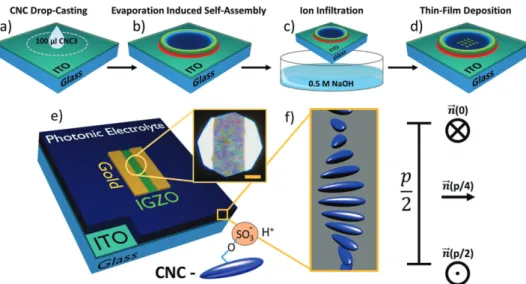
The CNCs used to prepare the photonic droplets were obtained through acid hydrolysis, as reported elsewhere.[21] The acid hydrolysis treatment reduces cellulose microcrys-tals into CNCs and additionally promotes a functionalization with sulfate half ester surface groups, which stabilizes the nanocrystals in suspension (as exemplified by one sulfate group in the inset in Figure 1e).[22] To enhance the volume fraction of the anisotropic phase, the resulting CNC suspen-sion was concentrated by centrifugation to 3 wt% with a pH of around 3 (CNC3).[23]
Figure 1 depicts schematically the fabrication process and the aspect of the final device. In order to fabricate the transistors on the CNC-based photonic electrolytes, an indium tin oxide (ITO)-coated glass serves as the substrate and common gate electrode, onto which 100 µL of the CNC suspension was drop-casted (see Figure 1a). After drop-casting, the circular films (d≈ 1.5 cm) are left to dry for one day in a controlled
environ-ment (25% relative humidity (RH), T= 21 °C) for EISA until
constant weight (see Figure 1b). The dry films were subse-quently subjected to an ion infiltration step, through submer-sion in 10 mL of 0.5 M NaOH for 1 h (see Figure 1c). Finally, after nitrogen drying, the amorphous indium-gallium-zinc-oxide semiconductor (a-IGZO), as well as the source and drain gold contacts (W/L = 2000 µm/50 µm), are deposited on top
of the films by physical vapor deposition (PVD) techniques, using shadow masks (Figure 1d). A schematic of the transistors is given in Figure 1e with a microscopic view on the channel
region. Figure 1f gives insight into the chiral nematic helicoidal superstructure of the solid-state photonic electrolyte.
Cellulose fibers naturally retain water in their structure, which serves as a protonic conductor through the Grotthuss mechanism, conferring electrolytic properties to it.[24] Conse-quently, paper can be used in FETs, taking the role of a solid-state electrolyte. Similarly CNCs can employ the same function to gate oxide thin-film transistors (TFTs).[21] One of the major drawbacks associated to these types of transistors is their need for high electric fields to promote ion polarization. This turns the transistors not only into high power dissipation devices but might also damage the deposited thin films, as was observed for our initial transistors with untreated CNC membranes (see Section S1 in the Supporting Information). Recently, low-voltage operation was achieved through alkali metal ion incorporation into cellulosic structures, serving as ion storage hosts.[25] In this study, we take advantage of this phenomenon by incorporating sodium ions from NaOH solutions into the chiral photonic CNC films through an ion infiltration process (as depicted in Figure 1c).
2.2. Photonic Solid-State Electrolyte Film
Chirality in CNC suspensions and dry films is believed to be imparted at mainly three distinct length scales; first at molec-ular scale from the cellulose chains (chiral glucose), second from the morphology of the CNC rods, and third by the long range order of the chiral nematic self-assembly.[26] The twisting with an intrinsic left handedness is therefore not only due to the inherent chirality of the individual cellulose chains but is also caused by morphological and liquid crystalline properties.[27]
The chiral nematic phase of the CNC suspensions is strongly related to interparticle electrostatic interactions, which have a substantial effect on the free energy of the system. The addition of salts or any form of ions to a CNC suspension destabilizes Figure 1. Schematic representation of device fabrication. a–d) The fabrication flow diagram is shown, whereas e) the final device structure with a microscopic view on the channel region of the transistor (scale bar indicates 25 µm) below an individual CNC nanoparticle and its negatively charged surface sulfate group is shown. f) The internal CNC superstructure with a twisted long-range order is illustrated, giving the droplet its photonic properties. The director (n
Supporting Information) until constant weight, regaining their initial thickness of 10 ± 1 µm (measured in the central region – see Section S4 in the Supporting Information). Chiral order is maintained and ion rich photonic electrolytes are obtained (atomic Na concentration in CNC:Na films of (0.99 ± 0.06)%, measured by energy-dispersive X-ray spectros-copy – EDS). For simplification, the Na-incorporated films will be treated as CNC:Na, whereas pristine films as CNC:0.
2.3. Optical Characterization
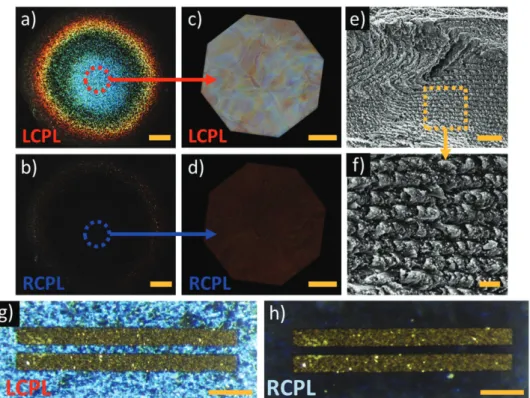
Both, the CNC:0 as well as the CNC:Na show a typical coffee-ring effect where the highest uniformity in thickness is obtained
ment of the CNCs. Upon solvent evaporation, the radial out-ward flow to the edge of the coffee ring induces CNC alignment which directly competes with the chiral nematic phase forma-tion and its kinetics.[34] Thus, the chiral nematic order increases when moving to the center of the droplet.[27] Having this phe-nomenon in mind together with film uniformity (Section S4, Supporting Information), the transistors were always deposited in the center regions of the photonic films in order to obtained strongest CPL response from the devices. Figure 2g,h depicts a microscopic view of one of the devices on top of a CNC:Na film in reflection mode for LCPL and RCPL, respectively.
The final devices showed an increased response when oper-ated in transmission mode, i.e., the highest CPL response was achieved when light passed first through the CNC:Na film
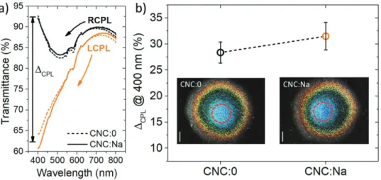
before reaching the photoactive a-IGZO layer of the transis-tors. In this mode, the CNC:Na films thus act as a photonic filter for CPL, blocking LCPL and transmitting RCPL. Thus, in order to quantify the spectral CPL response of the films, transmission spectrophotometry coupled with a circular polar-izer (EdmundOptics Plastic Circular Polarpolar-izer) was used. To decrease influences from the sin(θi) term from Equation (1), spectra were taken normal to the planar central region of the films. Figure3a shows a CPL transmission spectrum of a CNC:0 and a CNC:Na film for 400 nm ≤ λ≤ 800 nm, where the black and orange curves represent RCPL and LCPL, respectively. As expected, RCPL exhibits increased transmittance in the range between 80% and 90% for the investigated wavelength range. LCPL follows a similar trend starting from 800 nm until roughly 600 nm, from where it starts to diverge significantly from the RCPL data, indicating the start of the photonic bandgap.
The observed broad band transmission region (starting from 600 nm) is due to monodomains inside the film that form during the drying process (see Section S6 in the Sup-porting Information). These monodomains present distinct pitch values (P) which effectively influence the reflected
LCPL (Equation (1)) and thus the transmitted RCPL.[35] The maximum observed transmission however is centered at the average of coinciding domain orientation and pitch values. In the studied case (with the used CPL filters) the maximum distinction (∆CPL) between RCPL and LCPL lays at 400 nm. This value would be expected to further increase in the region
λ < 400 nm, which was not investigated (the used CPL filters are not superachromatic and thus going below 400 nm does not make sense – see Section S7 in the Supporting Informa-tion for data). Figure 3b plots and compares the achieved
∆CPL for each one of the films at maximum distinction. Here, we observe a maximum CPL distinction of around 30%, where no significant influence was measured between the pristine CNC:0 and the infiltrated CNC:Na, laying on average in the standard deviations of the measurements. These results show that the photonic properties and film anisotropies are retained during ion infiltration and the films can be used as
solid-state photonic electrolytes in FETs, yielding, what is com-monly known as electrolyte-gated transistors (EGTs).
2.4. EGTs on Solid-State Photonic Electrolyte
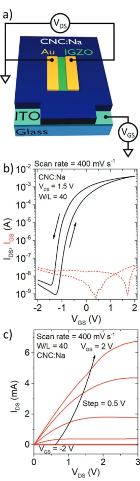
As stated beforehand, the ion incorporation has a variety of positive effects on the electrochemical activity but most impor-tantly, it was essential for the final devices, as with CNC:0 films, the EGTs showed no current modulation whatsoever. Transistors were deposited in the central regions of the films, where the highest uniformity in thickness and photonic proper-ties were achieved. The chosen staggered bottom-gate transistor architecture type (as depicted in Figure 4a) has considerable advantages when compared to planar types (where S/D and G lay in the same plane). Namely, faster ionic movement due to a vertical and thus more uniform electric field distribution in the CNC:Na film, leading to faster switching and lower opera-tion voltages.[36]
Figure 4b shows the transfer curves of the devices on CNC:Na which exhibit a typical n-type behavior at very low oper-ation voltages (VDS= 1.5 V for a symmetric VGS between −2 and
2 V), a counterclockwise hysteresis (indication for ionic charge accumulation at the interfaces) and a negative turn-on voltage (VOn). The screening of the negative charges of the pristine
CNC:0 from the Na+ ions shifts V
On to negative values, leading to a depletion mode (normally On) behavior. The devices show current On-Off ratios (IOn/IOff) of up to 7 orders of magnitude,
have never been achieved in paper-gated transistors. A possible explanation for this might lay in the structural order of the CNC membranes. For instance, activated, mesoporous, templated, or carbide-derived carbons with high specific surface area and ani-sotropy greatly increase electrolytic capacitance parameters.[37] However, there is little known on how mesoporosity or struc-tural order in the electrolyte itself might influence dielectric performance. Kim et al. worked with mesoporous silica as a single ion conducting solid-state electrolyte with directional anisotropy.[38] Their results show that ionic transport is facili-tated owing to the ordered structure. A similar effect could be in play here where the intrinsic chiral nematic order of the CNC:Na membranes enhances ionic polarizability. This positive “side effect” greatly enhances transistor performance, giving rise to these paper FETs with never before seen characteristics.
2.5. Circular Polarized Light Sensing
The photonic properties of the solid-state electrolyte in these devices confers an extra degree of freedom when it comes to information technology where now in addition to electric fields, CPL can influence distinct logic states. As already depicted in Figure 2g,h, the devices, when observed through CPL filters, exhibit very distinct microscopic aspects. A striking visible phe-nomenon, where successful sensing by means of an electronic device has yet to be achieved.
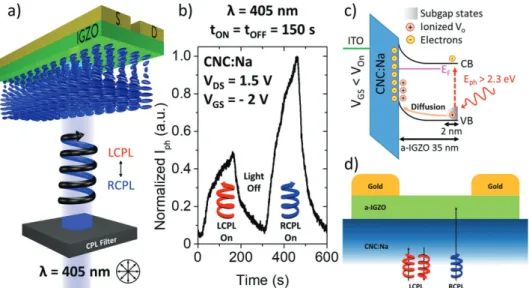
Figure 5a shows the employed setup for CPL detection
using the a-IGZO transistors on the CNC:Na photonic elec-trolytes. A blue light-emitting diode (LED) (λ = 405 nm) emits unpolarized light that attains circular polarization when transmitted through one of the CPL filters – LCPL for left-handed and RCPL for right-handed polarized light (see Section S7 in the Supporting Information for trans-mittance of the CPL filter). The CPL then travels through the glass/ITO substrate (for simplification not represented in the schematic), an isotropic medium that does not interfere with the polarization state. When reaching the CNC:Na film, the light, depending on the polarization state is either reflected back (LCPL) or transmitted (RCPL) to the semiconductor,
Figure 4. Electrical characterization of EGT on CNC:Na. a) Schematic representation of device architecture and applied voltages. b) Transfer
curves where continuous and dashed lines represent IDS and IGS,
respec-tively. c) Output curves for a VDS sweep from 0 to 3 V and distinct VGS
resulting in photoexcitation. Consequently, we expect a low current state for LCPL and a high current state for RCPL. In Figure 5b, we thus monitor subthreshold conduction of the devices with an applied VGS=−2 V < VOn when illuminated for
150 s either with LCPL or RCPL. A clear difference between the currents for LCPL and RCPL of up to 50% can be identified. Again, devices on CNC:0 showed slow response and only very low distinction of CPL, as efficient sensing is directly connected to transistor performance.
With the employed a-IGZO we face a wide bandgap (Eg≈ 3 eV ≈ 413 nm) semiconductor with excellent
photorespon-sivity in the visible to blue light spectrum, as confirmed by var-ious reports.[39,40] Photoexcitation in a-IGZO relies on the density of states (DOS), photoresponsive energies for sub-bandgap pho-tons and oxygen vacancies that create surface acceptors for holes. Even with photon energies (Eph) below Eg, electron–hole pairs
are photogenerated,[41] where the holes ionize oxygen vacancies to give Vo+ or Vo++ (which diffuse to the CNC:Na/a-IGZO inter-face) and the electrons remain in the conduction band (CB), yielding a photocurrent – Iph (see Figure 5c for a schematic
of the process). With transistors working in depletion mode (being the case of our devices), a negative bias stabilizes these photocurrents as no additional electrons flow into the semicon-ductor to deionize the defect states.
A response to the light stimulus is observed with similar rise and fall times for both polarization states. Interestingly, no persistent photoconductivity (PPC) is observed as IDS falls
back to the initial value after removal of the stimulus. A feat not observed during negative VGS measurements in n-type
amor-phous oxide semiconductors (AOS).[42] In our case, the leakage current at the CNC:Na/a-IGZO interface compensates the positive oxygen vacancies, minimizing PPC.
As confirmed by spectrophotometry, the highest ∆CPL for the investigated films was measured at λ= 405 nm (see Figure 3a), laying clearly in the order of subgap states of unpassivated
a-IGZO.[43] As an underlying phenomenon we can examine the optical paths through the CNC:Na layer for LCPL and RCPL. Figure 5d schematically illustrates distinct reflection or transmis-sion inside the CNC:Na film for LCPL and RCPL, respectively. In the LCPL case a portion of the light (ideally around 35% as con-firmed by spectrophotometry) will be reflected by the CNC:Na layer. Clearly, the photogenerated current for LCPL is nonzero as we are not dealing with a filter with perfect extinction coef-ficients owing to defects in the chiral nematic structure. On the other hand, for RCPL, around 90% of the light is transmitted and reaches the a-IGZO layer. This increases electron–hole pair photogeneration (especially for sub-bandgap states at the surface of the semiconductor), which in turn increases Iph.
It is noted that Iph doubles when comparing LCPL to RCPL.
This is surprising as ∆CPL was measured well below 50%. Fac-tors that might increase efficient distinction between the two states are for instance internal reflections of RCPL at interfaces, resulting in polarization inversion RCPL → LCPL which is then more easily reflected by the CNC:Na back into the light absorbing layers. An opposite effect might occur for the inverse case, where LCPL is polarization inversed upon reflection and then transmitted through the CNC:Na layer as RCPL light. We therefore might face a light trapping effect that can be an inter-esting point of study for future investigation.
3. Conclusion
In summary, we report on the integration of bioinspired pho-tonic films based on cellulose nanocrystals into transistor devices capable of sensing distinct polarization states of CPL.
To produce the final devices, an ion infiltration method was necessary to enrich the photonic CNC films with sodium ions from a sodium hydroxide solutions. It was shown that the infil-tration procedure does not disrupt chiral nematic ordering, Figure 5. CPL detection. a) A schematic representation of the implemented CPL detection setup. For simplification reasons the glass/ITO substrate is omitted. b) Normalized photogenerated current for a 150 s LCPL, 150 s off, and 150 s RCPL cycle. c) Band diagram of ITO/CNC:Na/a-IGZO. Sub-bandgap photons excite electrons from the valence band (VB) to the conduction band (CB) above the Fermi energy (EF) and ionize oxygen
information processing, where now not only light and electrons carry information but also distinct polarization states. The inte-gration of the presented devices into electronic circuitry with suited signal amplification could lead to an increase in sensi-tivity and a platform for logic CPL signal processing. Applica-tions range from spintronic devices (CPL spin induction into electrons), fiber optics, communication, imaging, or emission to sensing applications with CPL.
4. Experimental Section
CNC Preparation: CNCs were prepared by sulfuric acid hydrolysis (Sigma-Aldrich, 95–97%) of microcrystalline cellulose (Avicel PH-101, Sigma-Aldrich, 10 g).[21,23] Consecutive centrifugation steps were used
to obtain the final CNC suspension for certain pH values (1.9 and 3.9). Dialysis was used (Spectra/Pro 4 membrane) during 4 weeks to increase the final pH of the suspension until around 3.5. The obtained CNCs show 152 ± 65 and 17 ± 7 nm of length and width, resulting in an aspect ratio of 10 ± 3. These values are similar to previous works from the literature, which use the same experimental conditions.[44,45] Before drop-casting, to increase
anisotropy, the suspension was sonicated at least 3 times for 45 min.
CNC Film: To increase uniform spreading of the CNC suspension on the hydrophobic ITO surface, a UV/ Ozone exposure for 45 min was performed (PSD Series, Digital UV Ozone System by NOVASCAN). A mask with a circular opening of 1.5 cm was used, leaving the central area exposed to the treatment, while protecting the rest of the substrate. This way, after the UV exposure, the deposited CNC suspensions only spread until the limit of the treated area, forming the desired circular films. The films were left to dry for 24 h in a controlled environment (SICCO, 25% RH, T= 21 °C, measured by a TFA Dostmann/Wertheim humidity sensor) until constant weight. Ion infiltration was done in a Petri dish (diameter of 3 cm) using 10 mL of 0.5 M sodium hydroxide
solution from Sigma-Aldrich without any further purification. The samples with the films showing up were submersed in the solution and left for infiltration. After 1 h, the samples were extracted from the solution and rinsed off in ultrapure water for 3 s to remove residual hydroxide solution. Afterward, they were dried until constant weight using nitrogen flux. Thickness measurements were performed using a XP-200 profilometer from AMBIOS Technology. Surface scanning was performed with a speed of 0.1 mm s−1 and a stylus force of 1 mg over a
line length of 17 mm.
Macroimaging: For photographs of the films, a LEICA M80 magnifying lens was used with 0.25 × amplification. The software to obtain images from the LEICA IC80 HD camera was LEICA Microsystems Application Suite V4. Conventional plastic circular polarizing lenses (T > 40% for 400 nm < λ< 800 nm) from Edmund Optics were used to obtain images in RCPL or LCPL mode.
by the CNCs as gate dielectric, a-IGZO, working as the active oxide semiconductor and then titanium/gold (Ti/Au) source and drain electrodes deposited on top. The electrical contacts, double layer of Ti/Au with 6 and 65 nm, respectively, were deposited on the substrate by e-beam evaporation. The 35 nm IGZO (In2O3–Ga2O3–ZnO; 2:1:2 mol%)
layer was deposited by radio-frequency magnetron sputtering, at room temperature (RT), in an AJA ORION system. The semiconductor channel and the electrodes were patterned by shadow masks with a channel width (W) of 2000 µm and length (L) of 50 µm (W/L= 40).
Electrical Characterization and CPL Detection: Electrical characterization of the devices was conducted at RT using a Semiconductor Parameter Analyzer (Keithley 4200-SCS) and a manual probe station (JANIS ST-500). For the transfer curves, VGS was initially held at −2 V for 10 s
for stabilization and then swept in 0.1 V steps, from −2 to 2 V with a sweep delay (time interval between VGS points) of 0.25 s, with VDS= 1 V.
For output curves, VDS was swept from 0 to 3 V in 0.1 V steps for distinct
VGS between −2 and 2 V in 0.5 V steps, without sweep delay. For CPL
detection, the devices were illuminated from underneath by a λ= 405 nm LED from ThorLabs. Voltages were applied using microprobes.
Supporting Information
Supporting Information is available from the Wiley Online Library or from the author.
Acknowledgements
The authors acknowledge the support from the FCT – Portuguese Foundation for Science and Technology through the Ph.D. scholarship SFR H/BD/125191/2016. The authors would like to acknowledge the European Commission under project NewFun (ERC-StG-2014, GA 640598) and BET-EU (H2020-TWINN-2015, GA 692373). This work was also supported by the FEDER funds through the COMPETE 2020 Program, Portugal2020 project CelSmartSense number 17862 and the National Funds through the FCT – Portuguese Foundation for Science and Technology under the Project No. POCI-01-0145-FEDER-007688, Reference UID/CTM/50025, project FunPaper, reference EXPL/CTM-NAN/1184/2013, project PapEl, reference NAN/5172/2014, project PTDC/CTM-BIO/6178/2014 and M-ERA-NET2/0007/2016 (CellColor). S.N.F. acknowledges the MCTES, the European Social Funds, and the FCT for fellowships SFRH/BDP/78430/2011. D.G. acknowledges the support from the FCT – Portuguese Foundation for Science and Technology through the AdvaMTech PhD program scholarship PD/BD/52627/2014.
Conflict of Interest
Keywords
cellulose nanocrystals, circular polarized light, electrolyte-gated transistors, light sensing, photonic crystals
Received: July 31, 2018 Revised: September 11, 2018 Published online:
[1] G. F. Joyce, G. M. Visser, C. A. van Boeckel, J. H. van Boom, L. E. Orgel, J. van Westrenen, Nature1984, 310, 602.
[2] J. Cohen, Science1995, 267, 1265.
[3] J. Bailey, Origins Life Evol. Biosphere2001, 31, 167. [4] J. Podlech, Angew. Chem., Int. Ed.1999, 38, 477.
[5] T. H. Chiou, S. Kleinlogel, T. Cronin, R. Caldwell, B. Loeffler, A. Siddiqi, A. Goldizen, J. Marshall, Curr. Biol.2008, 18, 429. [6] Y. K. Takahashi, R. Medapalli, S. Kasai, J. Wang, K. Ishioka, S. H. Wee,
O. Hellwig, K. Hono, E. E. Fullerton, Phys. Rev. Appl.2016, 6, 1. [7] M. Grell, M. Oda, K. S. Whitehead, A. Asimakis, D. Neher,
D. D. C. Bradley, Adv. Mater.2001, 13, 577.
[8] J. Gilot, R. Abbel, G. Lakhwani, E. W. Meijer, A. P. H. J. Schenning, S. C. J. Meskers, Adv. Mater.2010, 22, E131.
[9] E. Ogut, G. Kiziltas, K. Sendur, Proc. IEEE2009, 160. [10] S. Richtberg, R. Girwidz, Phys. Teach.2017, 55, 406.
[11] K. Miyamoto, H. Wortelen, T. Okuda, J. Henk, M. Donath, Sci. Rep.
2018, 8, 10440.
[12] S. H. Lee, D. P. Singh, J. H. Sung, M. H. Jo, K. C. Kwon, S. Y. Kim, H. W. Jang, J. K. Kim, Sci. Rep.2016, 6, 1.
[13] W. Li, Z. J. Coppens, L. V. Besteiro, W. Wang, A. O. Govorov, J. Valentine, Nat. Commun.2015, 6, 1.
[14] Y. Yang, R. C. Da Costa, M. J. Fuchter, A. J. Campbell, Nat. Photonics
2013, 7, 634.
[15] J. P. F. Lagerwall, C. Schütz, M. Salajkova, J. Noh, J. H. Park, G. Scalia, L. Bergström, NPG Asia Mater.2014, 6, 1.
[16] R. H. Marchessault, F. F. Morehead, N. M. Walter, Nature1959,
184, 632.
[17] Y. Habibi, L. A. Lucia, O. J. Rojas, Chem. Rev.2010, 110, 3479. [18] E. Fortunato, N. Correia, P. Barquinha, L. Pereira, G. Goncalves,
R. Martins, IEEE Electron Device Lett.2008, 29, 988.
[19] L. Pereira, D. Gaspar, D. Guerin, A. Delattre, E. Fortunato, R. Martins, Nanotechnology2014, 25, 094007.
[20] S. N. Fernandes, P. L. Almeida, N. Monge, L. E. Aguirre, D. Reis, C. L. P. de Oliveira, A. M. F. Neto, P. Pieranski, M. H. Godinho, Adv. Mater.2017, 29, 1603560.
[21] D. Gaspar, S. N. Fernandes, A. G. De Oliveira, J. G. Fernandes, P. Grey, R. V. Pontes, L. Pereira, R. Martins, M. H. Godinho, E. Fortunato, Nanotechnology2014, 25, 094008.
[22] J.-F. Revol, L. Godbout, D. G. Gray, J. Pulp Pap. Sci.1998, 24, 146. [23] J. F. Revol, H. Bradford, J. Giasson, R. H. Marchessault, D. G. Gray,
Int. J. Biol. Macromol.1992, 14, 170.
[24] C. J. T. Grotthuss, Mémoire sur la décomposition de l’ eau et des corps, qu’ elle tient en dissolution a’ l’ aide l’ électricite galvanique; Vol 1, Rome 1805.
[25] I. Cunha, R. Barras, P. Grey, D. Gaspar, E. Fortunato, R. Martins, L. Pereira, Adv. Funct. Mater.2017, 27, 1606755.
[26] G. Chu, X. Wang, T. Chen, W. Xu, Y. Wang, H. Song, Y. Xu,
J. Mater. Chem. C2015, 3, 3384.
[27] A. G. Dumanli, H. M. van der Kooij, G. Kamita, E. Reisner, J. J. Baumberg, U. Steiner, S. Vignolini, ACS Appl. Mater. Interfaces
2014, 6, 12302.
[28] T. Furuta, E. Yamahara, T. Konishi, N. Ise, Macromolecules1996, 29, 8994.
[29] C. D. Edgar, D. G. Gray, Cellulose2001, 8, 5.
[30] X. M. Dong, T. Kimura, J.-F. Revol, D. G. Gray, Langmuir1996, 12, 2076.
[31] N. Lin, A. Dufresne, Nanoscale2014, 6, 5384.
[32] R. D. Deegan, O. Bakajin, T. F. Dupont, G. Huber, S. R. Nagel, T. A. Witten, Nature1997, 389, 827.
[33] J. H. Park, J. Noh, C. Schütz, G. Salazar-Alvarez, G. Scalia, L. Bergström, J. P. F. Lagerwall, ChemPhysChem2014, 15, 1477. [34] D. Gray, Nanomaterials2016, 6, 213.
[35] P. X. Wang, W. Y. Hamad, M. J. MacLachlan, Nat. Commun.2016,
7, 1.
[36] P. Grey, L. Pereira, S. Pereira, P. Barquinha, I. Cunha, R. Martins, E. Fortunato, Adv. Electron. Mater.2016, 2, 1500414.
[37] P. Simon, Y. Gogotsi, Nat. Mater.2008, 7, 845.
[38] Y. Kim, S. J. Kwon, H. K. Jang, B. M. Jung, S. B. Lee, U. H. Choi,
Chem. Mater.2017, 29, 4401.
[39] K. Ghaffarzadeh, S. Lee, A. Nathan, J. Robertson, S. Jeon, S. Kim, C. Kim, U.-I. Chung, J.-H. Lee, SID Symp. Dig. Tech. Pap.2011, 42, 1154. [40] A. Kiazadeh, H. L. Gomes, P. Barquinha, J. Martins, A. Rovisco,
J. V. Pinto, R. Martins, E. Fortunato, Appl. Phys. Lett. 2016, 109, 051606.
[41] K. Jeon, C. Kim, I. Song, J. Park, S. Kim, S. Kim, Y. Park, J. H. Park, S. Lee, D. M. Kim, D. H. Kim, Appl. Phys. Lett.2008, 93, 4.
[42] K. Ghaffarzadeh, A. Nathan, J. Robertson, S. Kim, S. Jeon, C. Kim, U. I. Chung, J. H. Lee, Appl. Phys. Lett.2010, 97, 2012.
[43] K. Nomura, T. Kamiya, H. Hosono, Appl. Phys. Lett.2011, 99, 2011. [44] W. Y. Hamad, T. Q. Hu, Can. J. Chem. Eng.2010, 88, 392.