A FEM Punch-Through IGBT Model
Using an Efficient Parameter Extraction Method
Rui Chibante
Armando Araújo, Adriano Carvalho
Instituto Superior de Engenharia do Porto (ISEP) Faculdade de Engenharia da Universidade do Porto (FEUP) Rua Dr. António Bernardino de Almeida, 431 Rua Dr. Roberto Frias, s/n
4200-072 Porto 4200-465 Porto
Portugal Portugal
[email protected] {asa, asc}@fe.up.pt
Abstract - A Finite Element physics-based punch-through
IGBT model is presented. The model’s core is based on solving the Ambipolar Diffusion Equation (ADE) trough a variational formulation, resulting in a system of ODEs. The approach enables an easy implementation into a standard circuit simulator SPICE by means of an electrical analogy with the resulting system of ODEs, solved as a set of current controlled RC nets that describes charge carrier distribution in low-doped zone. The issue of parameter extraction for physics-based IGBT models is also addressed. An optimisation-based algorithm enabling an efficient parameter extraction method for IGBT model is discussed. Model is validated comparing experimental and simulated results.
I. INTRODUCTION
Modeling charge carrier distribution, in low-doped zones, shown in all bipolar power semiconductor devices, is known as the most important issue for accurate description of dynamic behavior of these devices. Some accurate and complex models have been proposed but due to cumbersome implementation, models like those have been incorporated in powerful, but also very expensive ones, simulation programs (like SABER). Generalized use of physics based models by power circuit designers requires accurate device models running on inexpensive simulators, like those of standard SPICE family. So, in recent years several SPICE models have been reported in literature, with an interesting trade-off between accuracy and computation time. Besides Hefner’s reference model [1], the ADE Fourier based solution [2, 3] have shown interesting results. Although they are adequate for most circuit simulations conditions they present some inaccuracies in predicting dynamic carrier distribution. In Hefner’s model, calculation of redistribution current assumes a linear carrier distribution over n- region which causes some
problems at describing switching behavior at high blocking voltages [4]. In Fourier solution, series truncation can give rise to oscillations in carrier concentration which can affect voltage drop estimation [5, 6].
A new approach that overcomes the above limitations has been proposed recently [7, 8]. The core of this new model is based on Finite Element solution of ADE. The approach allows at solving ADE using a variational formulation and Finite Element Method (FEM) solution with one-dimensional simplex elements. The main advantage of the approach is an easy implementation of physics based models into general circuit simulators through electrical analogy with the
resulting system of ODEs, solved as a set of variable RC nets, describing hole/electron behaviour in low doped zone.
The success of this method has already been proved for PIN diodes, BJTs [9, 10] and non-punch-through (NPT) IGBTs [7, 8] and the aim of this paper is to extend the practice of this approach to punch-through (PT) structures.
Using standard models for other zones of the device (emitter, junctions, space charge and MOS) and with the knowledge of hole/electron time/space distribution and instantaneous base width, device’s currents and voltages are accurately determined. With this hybrid approach it is possible to describe device dynamic behaviour with high accuracy while maintaining low execution times.
Development and implementation into the standard circuit simulator SPICE of this new physics-based PT-IGBT model is presented in section 2.
The main drawback of physics based models is that they require extraction of numerous parameters. Model developers have recognized that an extraction scheme is crucial in order to design power circuits easily through simulation. Different papers in literature have addressed this issue for past decade.
Usually, proposed extraction methods are based on extrapolation of datasheet information and equations relating some parameters [2, 11, 12]. With this method they are not expected excellent results. Alternatively, some extraction procedures based on experimental measurements [13, 14] can give accurate results but they are very complex and require so precise measurements that they are not useful for needs of simulation [11, 13, 15]. As pointed out by Kraus et al. [16] probably the best approach is to combine previous methods to get an initial satisfying guess and then use parameter optimisation to extract optimum parameter set.
In recent publications parameter optimisation has been used successfully but with some drawbacks. In [17] parameters are extracted using an optimisation procedure by means of a relaxation algorithm. The algorithm is fast but requires a satisfying initial guess for model parameters and still some quite large errors are observed. In [18] a direct search technique is used to extract some parameters of the Fourier model. However, optimisation is neither based on current/voltage waveforms nor switching parameters. It is oriented to produce accurate power loss estimates by analyzing instantaneous power dissipation but it could happen that inaccuracies in voltage and current waveforms are mutually compensated.
optimisation algorithm (simulated annealing) described in [19] is further validated. This method is extremely simple to implement and has the advantage to converge to minimum even without a good initial guess. The method is theoretical computationally costly but results obtained so far show it is suitable for required purposes.
The algorithm requires only a few lines of code and can be implemented with any standard programming language. Optimisation procedure discussed in [19] is enhanced through a new cooling schedule developed in MATLAB. Finally, the FEM physics-based PT-IGBT model is implemented in IsSPICE.
The extraction procedure and IGBT (NPT and PT) model are validated with experimental and simulated results at different operating conditions.
II. FEM PHYSICS-BASED PT-IGBT MODEL
A. Finite Element approach of ADE
An implementation of a physics-based NPT-IGBT SPICE model was presented in [7, 8]. The core of this model is based on ADE solution, describing hole/electron behaviour in low doped IGBT base, trough a variational formulation. Application of Finite Element Method (FEM) to minimize the functional associated with ADE and boundary conditions results in a system of ODEs with symmetric matrices. So it is enabled a direct implementation of ADE solution, in time and space, in a standard circuit simulator like SPICE as a set of variable RC nets (Fig. 1) where current sources I1 and I2
implement boundary conditions. Because of moving boundary condition, resistors and capacitors in each RC net are a function of the effective base width WB(t).
As each RC net is associated with one part of the domain (the low-doped zone), that corresponds to FEM formulation for one element, voltages in each node of the net represent time evolution of hole/electron concentration in space.
Fig. 1 – RC network with n-1 one-dimensional elements.
A few sub circuits, based on classical approaches, modelling emitter, junctions, space charge and MOS regions of the device are developed in order to complete the IGBT model.
Details about implementation can be found in [7, 8, 10].
B. n- region modeling
Assuming a high-level injection condition for low-doped base zone the charge carrier distribution is given by the
well-known Ambipolar Diffusion Equation (ADE):
2 2 p p p D t
τ
x ∂ = − + ∂ ∂ ∂ (1)The general boundary condition associated with (1) is: 1 2 p n n p I I p x qA D D ⎛ ⎞ ∂ = − ⎜⎜ ∂ ⎝ ⎠⎟⎟ 2 (2)
where In/Ip are the electron/hole currents at the borders of the
n- region. Bipolar part of a one-dimensional PT-IGBT model
indicating the most important variables is presented in Fig. 2. Since from the current continuity equation:
0 0 1 1 2
T n p n p n p
I =I +I =I +I =I +I (3)
it is only necessary to define one current component for each side of the n+ zone and n- zone.
Fig. 2 – Bipolar diagram of PT-IGBT.
For an NPT-IGBT the electron current at the p+ emitter is
defined as: (4) 2 0 n p I =qAh pL0
where hp is the recombination parameter and electron current
at collector side (In2) is the channel current from MOS part of
the device.
C. Buffer layer modeling
Several papers in literature address this issue proposing several approaches. Effect of buffer layer is taken into account trough ADE boundary conditions but ADE solution depends mostly on n- region parameters [11] rather than on
n+ region parameters. On the other hand, buffer layer
parameters are generally extracted based on their empirical value range, so a simple description of the n+ region will not
compromise global model’s accuracy, avoiding possible convergence problems with a more complex solution, while
maintaining fast computation times.
The approach used here follows the model presented in [6] with minor modifications.
1) Boundary conditions
For a PT-IGBT model the existence of a buffer layer modifies the left (x = 0) boundary condition of ADE. Since buffer layer is a very high doped region, low-injection conditions are always valid and minority carrier current is obtained from integrating the continuity equation for holes, resulting in: 1 0 H H p p H Q dQ I I dt
τ
= − − (5)Ip0 is determined using again the current continuity condition and the h parameter theory:
2
0 0
p T p H
I =I −qAh N pH (6)
Assuming a linear distribution, the charge stored in buffer layer (QH) is determined by:
0 2 H HW H H p p Q =qAW + (7)
Hole concentrations in (7) can be related assuming that hole current flows only by diffusion. Following the linear approximation: 0 H HW H p p dp dx W − = (8)
and using the hole density equation:
0 p pH dp I qAD dx = (9)
hole concentration pH0 is expressed as
0 0 p H H HW pH I W p p qAD = + (10)
Finally, pHW is obtained using the quasi-equilibrium
approximation for n+/n- junction under high-level conditions
in the n- base: 2 0 L WH H p p N = (11)
Substituting (6), (7), (10) and (11), in (5) Ip1 is just a
function of pLO as in the NPT case. Buffer layer is completely
modelled using (5) in left boundary condition equation:
1 1 0 1 2 T p p x n p I I I p x = qA D D ⎛ − ⎞ ∂ = ⎜⎜ ∂ ⎝ − ⎠⎟⎟ (12) 2) Voltage drops
Using Boltzmann’s approximation, voltage drops at buffer layer’s junctions read:
0 2 ln H H T p n i p N V V n + + ⎛ ⎞ = ⎜ ⎝ ⎠⎟ (13) 0 ln B T n n L N V V p + − ⎛ ⎞ = ⎜ ⎝ ⎠⎟ (14)
III. PARAMETER EXTRACTION PROCEDURE
The PT-IGBT model requires 13 parameters from NPT structure plus 3 describing buffer layer (Table I).
TABLE I – PT-IGBT MODEL PARAMETER LIST Symbol Unit Description
A cm² Device active area
Agd cm² Gate-drain overlap area
WB cm Metallurgical base width
NB cm-³ Base doping concentration
hp cm4.s-1 Recombination parameter
τ s Base lifetime
Vtd V Gate-drain overlap depletion threshold
Cgs F Gate-source capacitance
Coxd F Gate-drain overlap oxide capacitance
Kf - Triode region MOSFET transconductance factor
Kp A/V² Saturation region MOSFET transconductance
Vth V MOSFET channel threshold voltage θ V-¹ Transverse field transconductance factor
WH cm Buffer layer base width
NH cm-³ Buffer layer doping concentration
τH s Buffer layer lifetime
The approach proposed in this paper uses an optimisation algorithm to perform the extraction: the simulated annealing algorithm. For the initial guess it is recommended to extract some parameters using techniques published in literature, for instance, gate charge curve given in datasheets to extract capacitances or some electrical measurements for MOS parameters (see [19] for details).
Because of large number of parameters a two-step strategy is used by dividing parameters in two groups: a first set of parameters is extracted using DC characteristics while second set is extracted using transient time waveforms with optimum parameters from DC extraction.
Optimisation is carried out by comparing simulated and experimental results from which an error value results. A
new parameter set is then generated and iterative process continues until parameter set converges to global minimum error.
A. Simulated annealing algorithm
Application of the annealing strategy is very simple and requires definition of two major steps:
• Objective function – a scalar equation to measure the goodness of each trial vector, that is, how good simulated data fits experimental data;
• Cooling schedule – a method that controls how
temperature decreases. Temperature is the main control
parameter and determines the algorithm’s evolution and performance.
Objective function is defined by comparing the error between simulated and experimental data. For DC optimisation it is measured the square relative error of each data point using at least 3 static curves of DC characteristics. For transient optimisation the influence of several error expressions as well as which waveforms to use were studied and better performance was obtained using absolute relative error of VCE and IC waveforms:
( ) ( ) ( ) s e i obj e c i i i g x g x f g x − =
∑∑
(15)where gs(xi) is the simulated data, ge(xi) is the experimental
data and c is the number of curves being optimised.
Note that this method requires only one simple set of experimental waveforms which can be obtained from a simple test circuit in a hard-switching configuration.
One disadvantage of simulated annealing is that definition of some control parameters (initial temperature, cooling rate, …) is somewhat subjective and must be defined from an empirical basis. The algorithm should be initially tested with several sets of control parameters to evaluate how they influence algorithm’s performance.
After this stage cooling schedule strategy was established with 5 iterations at each temperature and a constant rate for temperature cooling was adopted:
(16)
1 i
T+ =sTi
with s ranging from 0.90 to 0.99. Algorithm’s termination was done by setting a maximum number of iterations (300 to 500).
B. Optimisation results
IGBT models and parameter extraction procedure validation were carried out using a BSM200GA100D module
for NPT structure and a IRG4PC50U device for PT structure. As referred initial parameter estimates were done using techniques described in [19]. Tables II to V list starting conditions and optimum values found for DC and transient optimisation for both IGBTs.
TABLE II – CONDITIONS AND FINAL RESULT DC OPTIMISATION - BSM200GA100D Parameter (cm²) A Kf Kp (A/V²) Vth (V) τ (μs) (e-5θ V-¹) Initial value 2.67 1.6 39.5 5.45 25 3.3 Optimum value 2.76 0.87 32.7 5.51 29.8 1.15
TABLE III – CONDITIONS AND FINAL RESULT TRANSIENT OPTIMISATION - BSM200GA100D
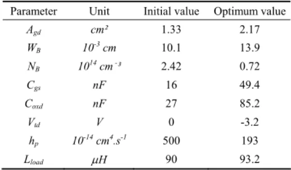
Parameter Unit Initial value Optimum value
Agd cm² 1.33 2.17 WB 10-3 cm 10.1 13.9 NB 1014 cm -³ 2.42 0.72 Cgs nF 16 49.4 Coxd nF 27 85.2 Vtd V 0 -3.2 hp 10-14 cm4.s-1 500 193 Lload μH 90 93.2
TABLE IV – CONDITIONS AND FINAL RESULT DC OPTIMISATION - IRG4PC50U Parameter (cm²) A Kf Kp (A/V²) Vth (V) τ (μs) (Vθ -¹) Initial value 0.27 1.8 7.5 5.00 1 0.050 Optimum value 0.283 1.93 7.5 5.25 0.57 0.049
TABLE V – CONDITIONS AND FINAL RESULT TRANSIENT OPTIMISATION - IRG4PC50U Parameter Unit Initial value Optimum value
Agd 10-2 cm² 6.75 7.8 WB 10-3 cm 8.7 7.6 NB 1014 cm -³ 1.95 1.94 Cgs nF 4 3.13 Coxd nF 7.1 5.26 Vtd V 0 -1.9 hp 10-14 cm4.s-1 5 6.2 Lload μH 90 91.2
Note that although procedure can be easily modified to take into account buffer layer parameters, they were not optimised and were set base on their empirical value range, since they do not have a significant effect on model accuracy [11].
IV. IGBT MODEL AND PARAMETER EXTRACTION VALIDATION
A. NPT validation
FEM NPT-IGBT SPICE model and parameter extraction procedure validation is performed by comparing experimental and simulated results using a BSM200GA100D module. Fig. 3 shows results for gate-emitter and collector-emitter voltages and anode current, using a test circuit in a hard-switching configuration, with VCC = 300 V, RL ≈ 30 Ω
and Rgate = 100 Ω. Bold lines represent experimental results.
0 2 4 6 8 10 12 (10 μs/div) Ic ( A ) 0 50 100 150 200 250 300 350 Vc e ( V) 0 2 4 6 8 10 12 (2 μs/div) Ic ( A ) 0 100 200 300 400 500 600 700 800 Vc e ( V)
Fig. 3 - Experimental and simulated transient curves at turn-on/off (top/bottom) (BSM200GA100D).
Simulated results at turn-on intentionally shifted for legibility.
For transient optimisation, although optimisation using only VCE produces good results, a better global fit of three
waveforms is obtained optimising both VCE and IC. Note that although curves are optimised only at turn-off a good agreement is obtained for whole switching cycle. This makes waveforms synchronisation a simple task.
The average relative error of some switching parameters values at turn-off is 5%. It is interesting to point out that an excellent error (2.9%) for turn-off losses is achieved without the need to optimise directly power losses.
B. PT validation
FEM PT-IGBT SPICE model validation is performed by comparing experimental and simulated results using a IRG4PC50U device in a test circuit with a hard-switching configuration, with VCC = 200 V, RL ≈ 30 Ω and Rgate = 100
Ω. Fig. 4 shows results for gate-emitter and collector-emitter
voltages and anode current. Bold lines represent experimental results.
Overall agreement is good and device’s behaviour is correctly captured. 0 2 4 6 8 (25 μs/div) Ic ( A ) 0 50 100 150 200 250 Vc e ( V) 0 2 4 6 8 (5 μs/div) Ic ( A ) 0 100 200 300 400 500 Vc e ( V)
Fig. 4 - Experimental and simulated transient curves at turn-on (top) and turn-off (bottom) (IRG4PC50U).
V. CONCLUSIONS
This paper presents a new hybrid PT-IGBT model based on a FEM formulation that accurately predicts charge carrier distribution in IGBT low doped base. Buffer layer effects are included using a quasi-static description.
An optimisation based procedure for parameter extraction of physics based power devices is reviewed.
Obtained results allow at concluding that:
1) Proposed method enables quick and efficient implementation of complete IGBT models in SPICE like circuit simulators.
2) It will be easy to apply the method to devices with similar structures, such as those presented in latest IGBT generations, like field stop [20] and CSTBT [21]), or thyristor-type devices like IGCT [22].
3) The used extraction algorithm is efficient for a large number of parameters needed for physics based IGBT models.
4) An accurate power loss prediction (Fig. 5) is possible optimising output voltage and current only at turn-off.
0 1000 2000 3000 4000 5000 (2 μs/div) P ( W ) 0 500 1000 1500 (2 μs/div) P ( W )
Fig. 5 - Experimental and simulated instantaneous turn-off power losses.
BSM200GA100D (top) ; IRG4PC50U (bottom). So converter design through simulation can be done with great flexibility and confidence.
VI. ACKNOWLEDGEMENT
This paper is partially supported by PRODEP III (Programa
de Desenvolvimento Educativo para Portugal) of Portuguese
Ministry of Education.
VII. REFERENCES
[1] C. S. Mitter, A. R. Hefner, D. Y. Chen, and F. C. Lee, "Insulated gate bipolar transistor (IGBT) modeling using IG-SPICE", IEEE
Transactions on Industry Applications, vol. 30, no. 1, pp. 24-33, 1994.
[2] P. Leturcq, J. Debrie, and O. Berraies, "A distributed model of IGBTs for circuit simulation", Proceedings of 7th European Conference on
Power Electronics and Applications (EPE'97), pp. 494-501, 1997.
[3] P. R. Palmer, J. C. Joyce, P. Y. Eng, J. Hudgins, E. Santi, and R. Dougal, "Circuit simulator models for the diode and IGBT with full temperature dependent features", Proceedings of 32th Annual IEEE
Power Electronics Specialists Conference (PESC'01), vol. 4, pp.
2171-2177, 2001.
[4] G. Busatto, F. Iannuzzo, and P. Grimaldi, "Lumped Charge PSPICE Model for High-Voltage IGBTs", Conference Record of the 35th IAS
Annual Meeting, vol. 5, pp. 2896-2902, 2000.
[5] X. Kang, X. Wang, L. Lu, E. Santi, J. L. Hudgins, and P. R. Palmer, "Physical modeling of IGBT turn on behavior", Conference Record of
the 38th IAS Annual Meeting, vol. 2, pp. 988-994, 2003.
[6] P. M. Igic, P. A. Mawby, M. S. Towers, W. Jamal, and S. Batcup, "Investigation of the power dissipation during IGBT turn-off using a new physics-based IGBT compact model", Microelectronics Reliability, vol. 42, no. 7, pp. 1045-1052, 2002.
[7] R. Chibante, A. Araújo, and A. Carvalho, "A new physics based SPICE subcircuit model for insulated gate bipolar transistors (IGBTs)",
Proceedings of 10th European Conference on Power Electronics and Applications (EPE'03), Toulouse, France, 2003.
[8] R. Chibante, A. Araújo, and A. Carvalho, "A new physics based SPICE model for NPT IGBTs", 29th Annual Conference of the IEEE Industrial
Electronics Society (IECON'03), pp. 1156-1161, Roanoke, United
States, 2003.
[9] A. Araújo, "Modelação de semicondutores bipolares - formulação de um novo método para simulação em circuitos electrónicos de potência," in Faculdade de Engenharia da Universidade do Porto. Porto, Portugal, 1998.
[10] A. Araújo and A. Carvalho, "SPICE implementation of a FEM based model for bipolar power semiconductors", Proceedings of 10th
European Conference on Power Electronics and Applications (EPE'03), Toulouse, France, 2003.
[11] X. Kang, E. Santi, J. L. Hudgins, P. R. Palmer, and J. F. Donlon, "Parameter extraction for a physics-based circuit simulator IGBT model", 18th Annual IEEE Applied Power Electronics Conference and
Exposition (APEC'03), vol. 2, pp. 946-952, Miami Beach, FL, United
States, 2003.
[12] J. Sigg, P. Turkes, and R. Kraus, "Parameter extraction methodology and validation for an electro-thermal physics-based NPT IGBT model",
Conference Record of the 32nd IAS Annual Meeting, pp. 1166-73 vol.2,
New Orleans, LA, USA, 1997.
[13] A. R. Hefner and S. Bouche, "Automated parameter extraction software for advanced IGBT modeling", 7th Workshop on Computers in Power
Electronics (COMPEL'00), pp. 10-18, 2000.
[14] A. Claudio, M. Cotorogea, and M. A. Rodriguez, "Parameter extraction for physics-based IGBT models by electrical measurements",
Proceedings of 33th Annual IEEE Power Electronics Specialists Conference (PESC'02), vol. 3, pp. 1295-1300, Cairns, Australia, 2002.
[15] P. O. Lauritzen, G. K. Andersen, and M. Helsper, "A basic IGBT model with easy parameter extraction", Proceedings of 32nd Annual IEEE
Power Electronics Specialists Conference (PESC'01), vol. 4, pp.
2160-2165, Vancouver, BC, Canada, 2001.
[16] R. Kraus and H. Mattausch, "Status and Trends of Power Semiconductor Device Models for Circuit Simulation", IEEE Trans.
Power Electron., vol. 13, no. 3, pp. 452-465, 1998.
[17] B. Allard, H. Morel, W. Mi, G. Hatem, K. Ammous, and D. Bergogne, "Systematic procedure to map the validity range of insulated-gate device models", Proceedings of 10th European Conference on Power
Electronics and Applications (EPE'03), Toulouse, France, 2003.
[18] A. T. Bryant, P. R. Palmer, J. L. Hudgins, E. Santi, and X. Kang, "The use of a formal optimisation procedure in automatic parameter extraction of power semiconductor devices", Proceedings of 34th
Annual IEEE Power Electronics Specialists Conference (PESC'03),
vol. 2, pp. 882-827, United States, 2003.
[19] R. Chibante, A. Araújo, and A. Carvalho, "A simple and efficient parameter extraction procedure for physics based IGBT models",
Proceedings of 11th International Power Electronics and Motion Control Conference (EPE-PEMC'04), Riga, Latvia, 2004.
[20] T. Laska, M. Munzer, F. Pfirsch, C. Schaeffer, and T. Schmidt, "The Field Stop IGBT (FS IGBT). A new power device concept with a great improvement potential", Proceedings of the 12th International
Symposium on Power Semiconductor Devices and ICs (ISPSD'00), pp.
355, 2000.
[21] Y. Tomomatsu, S. Kusunoki, K. Satoh, J. Yamada, Y. Yu, J. F. Donlon, H. Iwamoto, and E. R. Motto, "Characteristics of a 1200 V CSTBT optimized for industrial applications", Conference Record of the 36th
IAS Annual Meeting, vol. 2, pp. 1060, 2001.
[22] S. Bernet, E. Carroll, P. Streit, O. Apeldoorn, P. Steimer, and S. Tschirley, "Design, test and characteristics of 10 kV IGCTs",
Conference Record of the 38th IAS Annual Meeting, vol. 2, pp. 1012,