Direct Current Control of an Active Power Filter for Harmonic
Elimination, Power Factor Correction and Load Unbalancing
Compensation
Helder J. Azevedo, José M. Ferreira, António P. Martins, Adriano S. Carvalho
FACULTY OF ENGINEERING OF THE UNIVERSITY OF PORTO
Rua Dr. Roberto Frias, s/n, 4200-465, Porto, Portugal
Phone: +351 22 5081816; Fax: +351 22 5081443
e-mail: [email protected], [email protected]
Keywords
«Active filters, Converter control, Harmonics, Power factor correction»
Abstract
An active power filter is designed, simulated, implemented, and tested. It can work in different modes: active power filtering, power factor correction, and load unbalance compensation. It is based on a current controlled voltage-source inverter with fixed carrier PWM. The control algorithm generates the source reference currents based on the controlled DC link voltage. The dimensioning criteria of the inductive and capacitive power components is discussed. The implementation is validated with simulated and experimental results obtained in a 5 kVA prototype.
Introduction
Different solutions to minimize the effects of nonlinear loads in electric distribution systems (nonsinusoidal voltages, harmonic currents, nonbalanced conditions) have been proposed. However, it is desirable to achieve flexible AC power transmission systems, [1], [2], so incorporating power electronics circuits and other static compensators envisaging the increasing controllability and power transmission capacity.
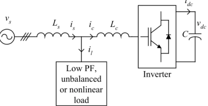
Different types of compensators have been proposed to increase the electric system quality, [1], [2], [3]. One of those compensators is the active power filter. Usually, the voltage-source is preferred to implement the parallel active power filter since it has some advantages, [1]. In this paper it is used the parallel topology, schematically shown in Fig. 1.
vs L s C idc vdc ic Low PF, unbalanced or nonlinear load Lc is il Inverter
Fig. 1. Diagram of a voltage source active power filter.
The filter generates currents in the connection point in order to cancel the harmonic content in the AC system, to correct the power factor, and to balance loads. So, the AC distribution system only carries the active fundamental component of the load current. A 5 kVA prototype of an active filter is designed, and tested in dynamic and stationary operation with different load types.
Active Filter Operating Modes
Very different control algorithms can be applied to the active filter, [4], [5], [6], [7]. The developed control system is based on a direct current control strategy that generates the reference waveform for the source current. It requires a low processing time and allows the calculation of the current reference with one of two strategies:
1- power factor correction, harmonic elimination, and load unbalance compensation or
2- voltage regulation, harmonic elimination, and load unbalance compensation, in the active filter connection node.
In this paper it was not implemented the voltage regulation since it is a concurrent objective faced to the power factor compensation. However, the control algorithm has enough flexibility to be configured, in real-time, to either objectives or for the two, in a weighted form. This flexibility is one the algorithm advantages. The current-controlled pulse width modulation with a 5 kHz fixed carrier ensures enough bandwidth to implement the active filtering.
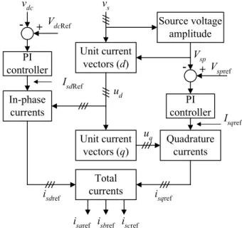
The control algorithm needs the measurement of several variables like the three phase AC source voltages and the DC link voltage. In order to impose sinusoidal currents in the source it is needed to low pass filter the AC voltage, so obtaining the fundamental component. The active power balance in the DC link determines the reference current of the AC source and the use of a PI controller allows a smooth control of the filter current and improves the system dynamic response. The main block diagram of the system operation is shown in Fig. 2. It implements the two referred control strategies being capable of dealing with load harmonics elimination, power factor correction, load unbalancing compensation, and/or voltage regulation.
vdc VdcRef IsdRef ud isdref vs Vsp Vspref Unit current vectors (q) Isqref uq isqref isaref isbref iscref
Total currents Unit current vectors (d) In-phase currents Source voltage amplitude Quadrature currents PI controller PI controller + -+
-Fig. 2. Diagram of the active power filter control modes.
Harmonic Elimination and Unbalance Compensation
As referred, in this paper it is implemented the first operating mode: power factor correction, harmonic elimination, and load unbalance compensation. So, the source power factor will be aproximately one, and there in no need to control the voltage at the connection point. In this case, the schematic in Fig.3 represents the essential block diagram of the current reference. The error in the DC voltage is transformed in active power to be controlled in the AC source.
VdcRef PI controller vdc vs Current controller isRef is + - + -icRef Gating pulses
Fig. 3. Block diagram for the calculation of the reference current.
Reference Current Determination
The rms source voltage amplitude, Vsp, is calculated from the source phase voltages, , , , as
expressed in (1). sa
v
v
sbv
sc 2 2 2 2( 3 ) sp sa sb s V = v +v +vc (1)The direct (or in-phase) unit current vectors are obtained from the source phase voltages and the rms amplitude of the source voltage,
V
sp./ / / sa sa sp sb sb sp sc sc sp u v V u v V u v V = = = (2)
The amplitude of the active component of the reference currents of the AC source, , , , is calculated through a PI controller with anti-windup as shown in Fig. 3. The proportional and integral gains determine the controller behavior in dynamic and static operation, [5], [7], [8], [9]. As stated before the correct active component,
* sad
i
* sbdi
* scdi
* spI , of the AC source current is determined from the power balance in the DC link. The current reference is then scaled with the unit current vectors in phase with the source voltage.
* * * * * * . . . sa sp sa sb sp sb sc sp sc i I u i I u i I u = = = (3)
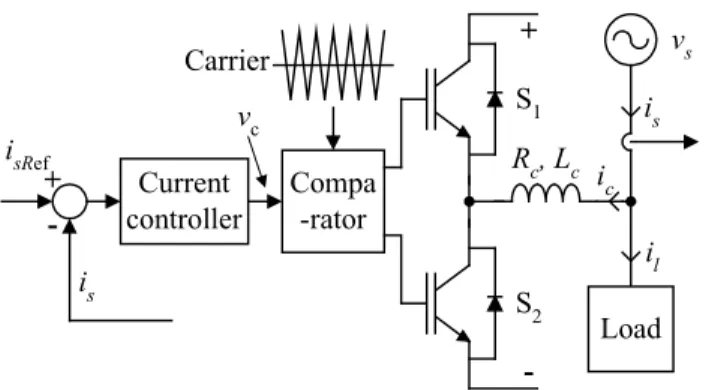
In the modulation stage (Fig. 4) the total reference currents are subtracted from the source current, obtaining a current error adapted according to the amplitude of the triangular carrier. The purpose of introducing the triangular waveform is to stabilize the converter switching frequency by forcing it to be constant and equal to the frequency of the triangular reference signal. Since the current error signal is alwyas kept within the the negative and positive peaks of the triangular waveform, the system has an inherent overcurrent protection. The PWM output is completed with the introduction of an appropriate dead time to the control signals of the inverter transistors.
Control Board Characteristics
The TERN 586-Engine, [10], is a module with a C++ programmable microprocessor. With a 32-bit CPU operating at 100 MHz it includes a math coprocessor for floating point operations. Several I/O interfaces are available, including 8 channel, 12-bit A/D converter; series D/A converter; 32 I/O lines; 15 external interrupts, and seven 16-bit timers.
S1 + -vc Rc, Lc Carrier isRef + -is Current controller Compa -rator S2 vs Load is il ic
Fig. 4. Current control and PWM stage.
Inductive and Capacitive Components
The selection of the AC link inductance and the DC capacitor values affects directly the performance of the active power filter performance. Static var compensators and active filters implemented with voltage-source inverters present the same power topology, but hte criteria used to select the values of
L and C are different.
Inductive Filter Design
One possibility to design the inductance is to consider the maximum current, Imax , that the filter must
supply in order to compensate a totally inductive load, which results in (4):
min 1 max. V L I ∆ = ω (4)
∆V is the difference between the source voltage and the inverter voltage, which depends on the values of the DC link voltage and the modulation index, and ω1 is the value of the source frequency. In order
to keep the ripple current at a reduced level, the used inductance value should not be less than this. As an active filter, the inductance value should be decreased to be capable of higher surge currents and harmonic currents. In this condition, another criteria can be evaluated, like the one referred in [11]. Imposing a fixed switching frequency, fc, the maximum di/dt of the current to be compensated, and the
ripple current, ∆i, the inductance value is now given by (5):
max max 4 c V L if ∆ = ∆ (5)
If the ripple can be reduced through an increasing in the switching frequency or an increasing in the controller dynamics the design of inductance value would not be so influent in the global filter performance. The connecting inductances also decouple the output inverter voltage from the AC source voltage. Considering, designing, and ranking all the referred factors, an indicative value for the inductance can be obtained.
DC Link Capacitor Design
In transient operation, some of the active power to be redirected by the filter is stored in the DC capacitor, corresponding to a high or low voltage variation in a more or less long charge or discharge periods. These variations are caused by transient regimes coming from changes in the instantaneous power absorved by the load. In the worst case of a totally inductive to totally capacitive compensation change, and considering the instantaneous power equal in both sides of the filter, Bojrup, [12], proposes a dimensioning criteria given by (6):
1 1 . 2 n dc dc S C V V = ∆ ω (6)
In (6), Sn is the filter nominal power, Vdc is the average DC voltage, ∆Vdc the predicted ripple voltage
and ω1 the AC frequency. The over/under voltage in limited, keeping the filter operating in good
conditions, namely maintaining the decoupling between the inverter output voltage phase and amplitude, and the output current. The value of the DC capacitor can also be designed in order to supply active power to the load during a defined time interval in case of AC source absence.
Simulation and Experimental Results
The SABER simulation software package was used to design, simulate, and test the filter control algorithm. In order to implement the algorithm in the TERN hardware platform it was built a simulation microcontroller model. So, the C code written and validated in SABER can be easily transferred to any hardware target.
Simulation Results
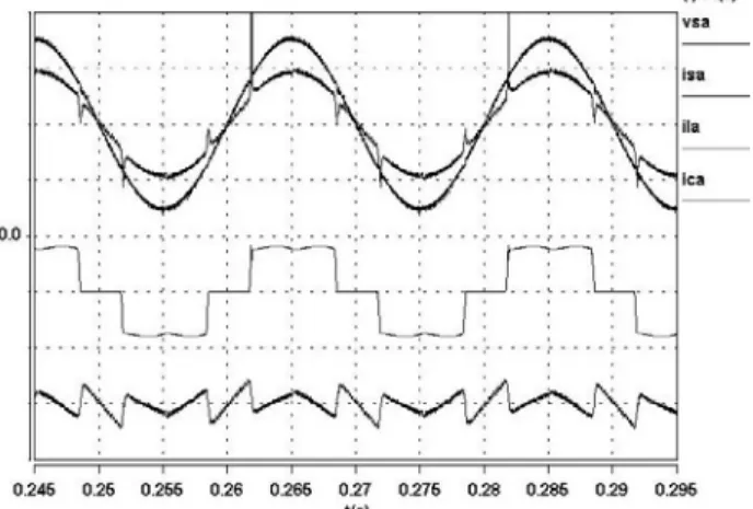
Different active filtering tests, power factor compensation, and load balancing tests have been done, in transient and static operation and for linear and nonlinear loads. The static operation tests were made putting the active filter in operation when the load was already connected to the AC source voltage. In Fig. 5 the nonlinear load is a three phase diode rectifier, with a DC current of 7 A and a DC voltage of 250 V.
Fig. 5. Static compensation of a three phase diode rectifier. Traces from top to bottom (phase A): source voltage, vsa , (100 V/div); source current, isa ,
(10 A/div); load current, ila , (10 A/div); filter current, ica , (10 A/div).
As can be seen, except for the high di/dt intervals, the active filter completely compensates the rectifier harmonic currents. A small inductance would produce a better compensation but with high ripple current.
The transient operation tests were made first connecting the filter and then connecting the load under test. In the case of Fig. 6 the load is again a three phase diode rectifier. It can be noted a short interval where the AC source current is out of phase with the voltage but it quickly gets in phase.
The simulation of the filter operation in load unbalance compensation is shown in Fig. 7. The load is a single phase diode rectifier bridge, connected between two phases; the third phase is an open circuit. Due to several factors the unbalance compensation is not perfect. It should be referred the DC voltage fluctuation caused by the unbalanced filter currents (if this condition would be the most important in the filter operation the DC capacitor value could be increased), and the effects of the assymetries in the AC inductances.
Fig. 6. Dynamic compensation of a three phase diode rectifier. Traces from top to bottom (phase A): source voltage, vsa , (100 V/div); source current, isa ,
(10 A/div); load current, ila , (10 A/div); filter current, ica , (10 A/div).
Fig. 7. Load unbalance compensation. Traces from top to bottom (phase A): source voltage, vsa , (100 V/div); source current, isa , isb , isc , (10 A/div); load
current, ila , (10 A/div); filter current, ica , (10 A/div).
Experimental Results
An experimental three phase active filter prototype has been designed for a nominal power of 5 kVA. It is based on a voltage source inverter with MOSFET transistors and a switching frequency of 5 kHz. Almost the same tests have been conducted and the results can be viewed in two perspectives: validation of the global simulation model, and measure of the active filter performance.
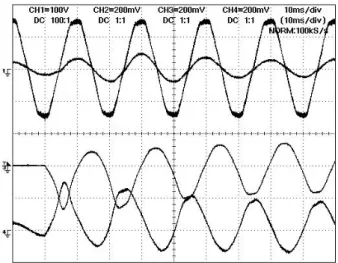
In Fig. 8 it can be seen the active filter behavior in a no-load induction motor magnetization. The filter quickly compensates the load power factor. The transient response is also dependent on the time interval where the load current has a non zero DC value.
The experimental tests were conducted in a laboratory with an important distortion in the mains voltage, due to the proximity of a large number of nonlinear loads. However, the mains current waveform after compensation is almost a sinewave due to the extraction of the fundamental component of the mains voltage through low pass filters. This filter action allows the imposition of sinewave references for the source current; it could be possible to impose non sinewave references “in phase” with the mains voltage.
Fig. 8. No-load induction motor magnetization. Traces from top to bottom (phase A): source voltage, vsa , (100 V/div); source current, isa , (20 A/div);
load current, ila , (20 A/div); filter current, ica , (20 A/div).
The nonlinear load shown in Fig. 9 is again a three phase diode rectifer. It can be seen that the mains current gets a sinewave form, being only slightly distorted in the instants of the diode switchings. This is due to the high di/dt occuring in these points, which is impossible to compensate unless with a very high DC voltage or a very low AC inductance. There should be a compromise between the active filter dimensioning and the characteristics of the load current to be compensated.
Fig. 9. Compensation of a three phase diode rectifier. Traces from top to bottom (phase A): source voltage, vsa , (100 V/div); source current, isa , (20
A/div); load current, ila , (10 A/div); filter current, ica , (10 A/div).
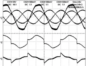
In Fig. 10 it is presented the symmetrical action of the active filter compensating an unbalanced load (a single phase diode rectifier bridge, connected between two phases; the third phase is an open circuit.).
Conclusions
The implemented active power filter has high performance characteristics, operating in active filtering, power factor compensation, and load unbalance compensation. It estimates and imposes sinewave current references even in the case of highly distorted mains voltage. In transient operation the unity power factor is obtained immediatly. The presented implementation has been validated and can be applied in different operating modes: harmonic active filtering, power factor correction, and balancing
of linear or nonlinear loads, single or grouped, which cause great perturbation and performance degradation in the power quality of an electrical distribution system.
Fig. 10. Load unbalance compensation. Traces from top to bottom (phase A): source voltage, vsa , (100 V/div); source current, isa , isb , isc , (10 A/div);
load current, ila , (10 A/div); filter current, ica , (10 A/div).
Appendix
Nominal power: 5 kVA
Mains voltage: 110/190 V, 50 Hz DC voltage: 500 V
Switching frequency: 5 kHz; dead time: 7 µs
Ls, Rs: 10 mH; 0.7 Ω
Lc, Rc: 2 mH; 0.2 Ω
DC capacitor: 1.6 mF
KP, KI: 0.5; 1.0
References
[1]. M. H. Bollen, “Understanding Power Quality Problems: Voltage Sags and Interruptions”, Wiley-IEEE Press, 1999.
[2]. N. G. Hingorani, L. Gyugyi, “Understanding Facts: Concepts and Technology of Flexible AC Transmission Systems”, Wiley-IEEE Press, 1999.
[3]. H. Fujita, H. Akagi “The Unified Power Flow Conditioner: The Integration of Series- and Shunt-Active Filters”, IEEE Transactions on Power Electronics, Vol.13, Nº2, pp.315-322, 1998.
[4]. J. W. Dixon, G. Venegas, L. Morán, "A Series Active Power Filter based on a Sinusoidal Current-Controlled Voltage-Source Inverter", IEEE Transactions on Industrial Electronics, Vol.44, Nº5, pp.612-620, 1997.
[5]. A. Chandra, B. Singh, B. N. Singh, K. Al-Haddad, “An Improved Control Algorithm of Shunt Active Filter for Voltage Regulation, Harmonic Elimination, Power Factor Correction and Balancing of Nonlinear Loads", IEEE Trans. on Power Electronics, Vol.15, Nº3, pp.495-507, 2000.
[6]. P. Verdelho, G. D. Marques, “An Active Power Filter and Unbalanced Current Compensator”, IEEE Transactions on Industrial Electronics, Vol.44, Nº3, pp.321-328, 1997.
[7]. S. Buso, L. Malesani, P. Mattavelli, “Comparison of Current Control Techniques for Active Filter Applications”, IEEE Transactions on Industrial Electronics, Vol.45, Nº 5, pp.722-729, 1998.
[8]. C. Schauder, H. Mehta, “Vector Analysis and Control of Advanced Static VAR Compensators”, IEE Proceedings, Part C, Vol.140, Nº4, pp.299-306, 1993.
[9]. A. P. Martins, A. S. Carvalho, A. S. Araújo, “Modelling and Simulation of a Voltage Source Three Phase Active Power Filter”, Proceedings of the European Simulation Congress, EUROSIM ‘95, Vienna, pp.735-740, 1995.
[10]. TERN Inc., “586-Engine – Technical Manual”, Davis, USA, 2000.
[11]. L. A. Morán, J. W. Dixon, R. R. Wallace, “A Three-Phase Active Power Filter Operating with Fixed Switching Frequency for Reactive Power and Current Harmonic Compensation”, IEEE Transactions on Industrial Electronics, Vol.42, Nº4, pp.402-408, 1995.
[12]. M. Bojrup, “Advanced Control of Active Filters in a Battery Charger Application”, Lund University, Sweden, 1999.