Marian Gaiceanu, Cristian Nichita
dSPACE I mplementation of the Third Harmonic
I nsertion based Modulation on the Three Phase
Pow er I nverter
This paper shows the implementation of real-time modulation based on the third order harmonic insertion in three-phase power inverter. Two methods of implementation have been proposed. As a working methodology the mathematical model of the duty cycles of the
three-phase power inverter have been designed and implemented in
Mat-lab/ Simulink® . By an adequate design the appropriate ControlDesk interface send the adequate signals to power inverter and collect all the necessay data to be viewed. Harmonic analysis has been performed. The advantages of using this type of modulation are highlighted.
Keyw ords: power inverter, Matlab Simulink, dSpace, third harmonic insertion
1. I ntroduction
Modern energy conversion systems are based on power converters [ 1] -[ 3] . The efficiency of the power converters can be improved by using adequate modu-lation techniques [ 1] , [ 2] , [ 4] . The advantages of the third harmonic insertion as modulating signal of power inverters are shown in this paper. The Sinusoidal PWM technique conducts to low DC bus utilization, therefore low efficiency. By adding a triple frequency term the DC link voltage usage increase; in this way boosting the drive efficiency.
Two methods of third harmonic insertion have been developed [ 2] , [ 5] by deducting the maximum amplitude of the signal. Taking into account the limit of the modulating signal, t he feasible solution has been selected.
2. First approach
By inserting the third–harmonic PWM the modulating waveform becomes:
t
sin
θ
K
sin
3
θ
y
(1)where: -the phase, K- the unknown parameter, has to maintain the limits of the
y
t
signal up to 1.Through the optimization process t he Kparameters will be found. By deriva-ting the signal
y
t
respect to angle θand equating to zero, the maximumampli-tude of the
y
t
signal can be found.
0
3
cos
3
cos
θ
θ
θ
θ
d
t
dy
K
d
t
dy
(2)
To develop the
cos
3
θ
in terms ofcos
θ
, it could be considerate:
θ
θ
θ
cos
2
3
cos
, (3)and taking into account that
θ
θ
θ
θ
cos
sin
2
2
sin
1
cos
2
2
cos
2
x
, (4)
the following useful expression can be found:
θ
θ
θ
4
cos
3
cos
3
cos
3
(5)By introducing (5) in (2) and equating to zero, after some elementary calculus the following expression should be found:
1
3
4
cos
3
0
cos
θ
K
2θ
(6)or in the final form:
12
cos
9
1
0
cos
2
K
K
θ
θ
(7)The above deducted equation (7) has two solutions:
0
9
1
0
cos
12
2
K
K
θ
orK
K
12
1
9
cos
θ
(8)I n order to find the solutions in terms of
sin
θ
, the following equation has to be considered:θ
θ
2cos
1
sin
. (9)I n this way, two conditions in
sin
θ
expressions could be found:1
sin
θ
(10)K
K
12
3
1
sin
θ
.
(11)
I n the same manner with eq. 5:
θ
θ
θ
2sin
4
3
sin
3
sin
. (12)From eq. (1), by introducing (5) results:
y
t
K
θ
θ
θ
2sin
4
3
sin
3
sin
(13)or in the form
K
K
θ
y
t
θ
3sin
4
3
1
sin
(14)According to the first solution (10), sinθ 1, by replacing it into (14), the maximum value of the signal y(t) is obtained for
K
yˆ1 (15)
By using the second solution (11), the maximum value of the y signal (14) could be
312
3
1
8
ˆ
K
K
K
t
y
(16)I n order to find the optimum value of the Kparameter, the first derivative of the maximum value of the
y
ˆ
(t) signal is computed:
0
ˆ
dK
t
y
d
i.e.
0
3
1
2
12
3
1
21
K
K
K
. (18)
The first solution
3
1
K
(19)conduct to the maximum amplitude signal,
1
ˆ
t
y
. (20)Therefore, only the second solution
6
1
K
(21)will maintain the maximum amplitude of the signal
y
ˆ
t
1
, i.e.
θ
sin
3
θ
6
1
sin
t
y
. (22)By replacing (21) in (8), the following result is obtained:
2
1
cos
θ
or3
π
θ
n
,n
1
,
. (22a)I ntroducing
3
π
θ
n
in (22), the maximum value of they
ˆ
t
amplitude isfound:
2
3
ˆ
t
y
. (23)According to (23) the maximum value of the modulating waveform decreased
by
2
3
, while the amplitude of the fundamental is unity.
I n order to increase the efficiency of the power inverter, the utilization of the DC link voltage can be increased:
θ
sin
3
θ
6
1
sin
R
t
y
, (24)where R has to be determined.
The amplitude of the modulating signal is increased at unity by introducing the condition:
1
ˆ
t
y
, (25)which means
3
Considering n= 1 and combining the above mentioned conditions (25), from eq. 24 becomes the value of the R parameter can be found:
1= R
2
3
or3
2
R
(26)By introducing the third harmonic, the obtained three phase modulating sig-nals are as follows:
θ
sin
3
θ
6
1
sin
3
2
*
t
u
A
θ
π
sin
3
θ
6
1
3
2
sin
3
2
*
t
u
B (27)
θ
π
sin
3
θ
6
1
3
4
sin
3
2
*
t
u
CThe advantages of using the three phase modulating signals (27) are: in-creased DC link voltage utilization and the inin-creased amplitude of the modulating signals while the amplitude of the fundamental is increased by 15,5 % .
3. Second approach
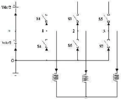
I n the Fig. 1 the basic power inverter schematic, supplying a three-phase load, is shown. I t consists of six power switching devices (I GBTs), S1, S3, S5 makes the upper bridge, and S4, S6, S2 the lower bridge. There are three arms, the power semiconductor devices on one arms cannot conduct simultaneously.
The most common modulation used method is sinusoidal pulse width modula-tion (PWM). The PWM method introduces an important advantage: generates the high order harmonics, therefore the lower filter inductance is obtained in order to compensate them.
Figure 1.Three-phase power inverter schematic.
*
,10 ,1 ,1 ,2 ,3 ,1 ,2 ,3
1
max
,
,
min
,
,
2
2
dc
s s n s n s n s n s n s n s n
V
v
v
v
v
v
v
v
v
(28)
*
,20 ,2 ,1 ,2 ,3 ,1 ,2 ,3
1
max
,
,
min
,
,
2
2
dc
s s n s n s n s n s n s n s n
V
v
v
v
v
v
v
v
v
(29)
*
,30 ,3 ,1 ,2 ,3 ,1 ,2 ,3
1
max
,
,
min
,
,
2
2
dc
s s n s n s n s n s n s n s n
V
v
v
v
v
v
v
v
v
(30) Considering phase 1, during on one sampling period Tc, the DC voltage, Vdc,
is applied when S1 switch is ON, during ton= t +, and a zero voltage is applied
dur-ing toff =t -, S4 being ON, such that
* ,10
0
dc s c
V t
t
v
T
(31) By taking into consideration the voltage symmetry:
,1 ,2 ,3
0
s n s n s n
v
v
v
(32)
From the eq. (31) the adequate duty factor on phase 1 is obtained:
,1 *
1 ,1 ,2 ,3 ,1 ,2 ,3
1
1
max
,
,
min
,
,
2
2
s n
s n s n s n s n s n s n
dc dc
v
d
v
v
v
v
v
v
V
V
(33)
Similarly, the duty factors for the other two phases are obtained:
,2 *
2 ,1 ,2 ,3 ,1 ,2 ,3
1
1
max
,
,
min
,
,
2
2
s n
s n s n s n s n s n s n
dc dc
v
d
v
v
v
v
v
v
V
V
(34)
,3 *
3 ,1 ,2 ,3 ,1 ,2 ,3
1
1
max
,
,
min
,
,
2
2
s n
s n s n s n s n s n s n
dc dc
v
d
v
v
v
v
v
v
V
V
(35)
4. Simulation results
I nitial data: DC-link voltage Vdc= 310V; sample time tA= 0.0001s; commutation
cycle Tc= 2* tA; PWM frequecy fPWM= 1/ (2* tA); inductive load Ls= 0.03 H; Rs= 50 ;
Rf= 10.
Simulink implementation
0 0.005 0.01 0.015 0.02 0.025 -400 -200 0 200 400 time [s] v s 1 N P W M , v s 1 N [ V ]
0 0.005 0.01 0.015 0.02 0.025 0 100 200 300 400 time [s] v s N O P W M , v s N O [ V ]
0 0.005 0.01 0.015 0.02 0.025 0 100 200 300 400 time [s] v s 1 O P W M , v s 1 O [ V ]
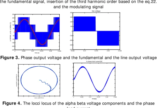
Figure 2.The output phase voltage of the three-phase power inverter and
the fundamental signal, insertion of the third harmonic order based on the eq.22. and the modulating signal
0 0.005 0.01 0.015 0.02 0.025 -250 -200 -150 -100 -50 0 50 100 150 200 250 time [s] v s 1 N P W M , v s 1 N , v s 1 N fi lt e r [V ]
0.005 0.01 0.015 0.02 0.025 -400 -300 -200 -100 0 100 200 300
400 line voltage
Figure 3.Phase output voltage and the fundamental and the line output voltage
-4 -3 -2 -1 0 1 2 3 4 -4 -3 -2 -1 0 1 2 3 4
isalfa, isalfaPWM [A]
is b e ta P W M , is b eta P W M [ A ]
0 0.005 0.01 0.015 0.02 0.025 -4 -3 -2 -1 0 1 2 3 4
A phase load current [A]
time[s]
Figure 4.The locci locus of the alpha beta voltage components and the phase
load current
0.005 0.01 0.015 0.02 0.025 -400
-200 0 200
400 Phase load voltage va
0.005 0.01 0.015 0.02 0.025 -400
-200 0 200
400 Phase load voltage vb
0.005 0.01 0.015 0.02 0.025 -400
-200 0 200
400 Line RL load voltage vab
0 5 10 15 20 25 30 35 40 45 50 0
50 100 150
200 vao
0 5 10 15 20 25 30 35 40 45 50 0
50 100 150
200 vbo
0 5 10 15 20 25 30 35 40 45 50 0
100 200
300 vab
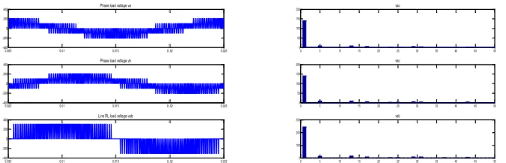
Figure 5.Three phase output modulated voltage and the harmonic spectrum
of the three phase load current
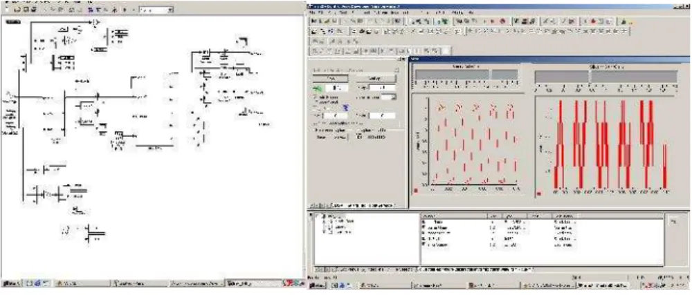
5. I mplementation on the dSPACE platform
I n the Fig. 3 the imposed dut y cycle for generating PWM waveform is shown. According to Fig.4, the imposed duty cycle for generating PWM waveform with third order harmonic insertion is shown
PWM duty cycle re fe re nce
3 d3*
2 d2*
1 d1*
Saturation 0 1 Saturation
-0.5 0.5 1/Vdc
1/Vdc 1/Vdc
emu
0.5*[1 1 1] 3
vs3N 2 vs2N
1 vs1N
duty_cycle*= vs1O/Vdc=(vs1N+Vdc/2)/Vdc
Figure.6PWM implementation by using the imposed duty-cycle d*1, d*2,d*3
duty_cycle1*=v1O/Vdc=
[vs1N+Vdc/2-(max(vs1N,vs2N,vs3N)+min(vs1N,vs2N,vs3N))/2]/Vdc
DUTY CYCLE - Third harm onic ins e rtion
3 d3*
2 d2*
1 d1*
Tc Tc
Tc
Saturation 0 1
Saturation -1/sqrt(3) 1/sqrt(3)
max min
1/Vdc 1/Vdc 1/Vdc
.5
emu
0.5*[1 1 1]
3 vs3N
2 vs2N
1 vs1N
Figure.7 Third harmonic insertion by using the imposed duty-cycle
d*1,d
* 2,d
* 3
Taking into consideration a DC link voltage Vdc= 10V, RL load with Ls= 0.03H;
Rs= 50; filter Rf= 10 and a sample time of 0.1ms, based on the Fig.3 an
Figure 8.ControlDesk interface for the third harmonic implementation
Adequate harmonic analysis of the load current reveals the influence on the phase and line voltages (Fig.5). The most important harmonics are 5th, 13th and 17th. Therefore a low size RL filter should be designed in order to decrease the harmonics content.
6. Conclusions
The third harmonic insertion increases the power converter efficiency by in-creasing the DC link voltage utilization and the amplitude of the fundamental is increased by 15,5 % .
Two implementation methods of the third harmonic insertion have been con-siderate.
By using the dSpace platform, the adequate duty cycle has been implemented through the ControlDesk.
Acknow ledgment
This work was supported by a grant of the Romanian National Authority for Scientific Research, CNDI –UEFI SCDI , project number PN-I I -PT-PCCA-2011-3.2-1680.
References
[ 1] Kazmierkowski M.P., Krishnan R., Blaabjerg F., Control in Power
Elec-tronics: Selected Problems, Academic Press Series in Engineering, 2003
[ 2] Keliang Zhou, Danwei Wang, Relationship between Space-Vector
Mod-ulation and Three-Phase Carrier-Based PWM: A Comprehensive Analysis,
I EEE Transactions on I ndustrial Electronics, VOL. 49, NO. 1, FEBRUARY 2002, pp. 186-196
[ 3] Stumpf P., Jardan R.K., Nagy I ., Comparison of Naturally Sampled
PWM Techniques in Ultrahigh Speed Drives, I SI E 2012, pp.246-251
[ 4] Pereira I ., Martins A., Experimental Comparison of Carrier and Space
Vector PWM Control Methods for Three-Phase NPC Converters, I
nterna-tional Conference on Renewable Energies and Power Quality (I CREPQ’09), Valencia, Spain, 15th to 17th April, 2009.
[ 5] Satputaley R.J., Borghate V.B., Bharat Kumar, M. A. Chaudhari, Third
Harmonic I njection Technique for Dynamic, Voltage Restorer with
Repeti-tive Controller, ASAR I nternational Conference, Bangalore Chapter- 2013,
pp.28-34
Addresses:
Assoc. Prof. Dr. Eng. Marian Gaiceanu, “Dunarea de Jos” University of Galaţ i, Domneasca Street, nr. 47, 800008, Galaţ i,
Prof. Dr. Eng. Cristian Nichita, University of Le Havre, 25 rue Philippe Lebon, BP 1123, 76 063 Le Havre CEDEX, FRANCE,