Automatic Generation of Cellular Automata on FPGA
Andr´e Costa Lima
Faculdade de Engenharia
Universidade do Porto
[email protected]
Jo˜ao Canas Ferreira
INESC TEC and Faculdade de Engenharia
Universidade do Porto
[email protected]
Abstract
Cellular automata (CA) have been used to study a great range of fields, through the means of simulation, owing to its computational power and inherent characteristics. Fur-thermore, CAs can perform task-specific processing. Spa-cial parallelism, locality and discrete nature are the main features that enable mapping of CA onto the regular archi-tecture of an FPGA; such a hardware solution significantly accelerates the simulation process when compared to soft-ware. In this paper, we report on the implementation of a system to automatically generate custom CA architectures for FPGA devices based on a reference design. The FPGA interfaces with a host computer, which initializes the sys-tem, downloads the initial CA state information, and con-trols the CA’s operation. The user interface is are provided by a user-friendly graphical desktop application written in Java.
1. Introduction
Cellular automata have already been studied for over half a century. The concept was introduced by John von Neumann in the late forties when he was trying to model autonomous self-replicating systems [1]. Since then, CA-based architectures have been extensively explored by the scientific community for studying the characteristics, pa-rameters and behaviour through simulation of dynamic complex systems, natural and artificial phenomena, and for computational processing [2]. Specific-application ar-eas are, e.g., urban planning, traffic simulation, pseudo-RNG, complex networks, biology, heart modeling, image processing, sound waves propagation and fluid dynamics. Furthermore, CA is also a possible candidate for future al-ternative computer architectures [3].
Nowadays, the need for creating simulation environ-ments of a high degree of complexity to describe rigorously the complete behaviour of a system, and for developing al-gorithms to process data and perform thousands of calcu-lations per second, typically incurs a high computational cost and leads to long simulations. Taking advantage of multi-core architectures, with parallel programming, to as-sign multiple task execution to different threads, enables significant software optimizations and accelerated execu-tion. However, parallel programming in software is a
com-plex task, as several aspects such as concurrency must be taken into account, and may be time-consuming. CA of-fer simplicity when it comes to define each cell’s func-tionality and owing to its inherent massive spacial paral-lelism, locality and discrete nature, such systems are natu-rally mapped onto the regular architecture of an FPGA, or-ganized in reconfigurable logic blocks; it is possible to per-form complex operations with efficiency, robustness and, most importantly, decrease drastically the simulation time with high-speed parallel processing. Thus, as a reconfig-urable hardware device, FPGA platforms are a very good candidate for CA architecture implementations on hard-ware: each cell functionality can be implemented in look-up tables, its state stored in flip-flops or block-RAM, and it is possible to update the state of a set of cells in parallel every clock cycle.
In this paper, we report on the implementation of a sys-tem to automatically generate CA architectures on a tar-get FPGA technology, a Spartan6, the characteristics and rules of which are specified by the user through a software application, that also allows controlling the operation, ini-tializing and reading the state of the CA. The implementa-tion results show that it is possible to achieve a speed-up of 168, when comparing to software simulations, for a lattice size of 56×56 cells for the Game of Life [4] [5]. Further-more, we achieved lattice dimensions of 40×40 and 72×72 cells for the implementation of a simplified version of the Greenberg-Hastings [6] and lattice gases automata [7], re-spectively.
The remainder of the paper is organized as follows. Sec-tion 2 introduces the key characteristics and properties of CA. Section 3 presents some of the existing work related to implementations of CA in FPGA platforms. Section 4 describes the overall system architecture, its features and specification. In section 5 the implementation results are summarized and discussed. Finally, section 6 concludes this paper and future developments are proposed.
2. Cellular automata
Cellular automata are mathematical models of dynamic systems that evolve autonomously [8]. They consist in a set of large number of cells with identical functionality with local and uniform connectivity, and organized in a regular lattice with finite dimensions [9], for e.g., an array a matrix
or even a cube for the multidimensional scenario; bound-ary conditions, that can be fixed null or periodic (the lattice is wrapped around), define the neighbourhood of the cells located at the limits of the lattice. For square-shaped cells, the neighbourhood is typically considered to be of Moore [10] or von Neumann [11] types which are applicable to 2D and 3D lattices; considering a single cell, the local neigh-bourhood is defined by the adjacent cells surrounding it, i.e. the first order or unit radius neighbourhood. Thus, for 2D lattices, the Moore-type neighbourhood includes all the 8 possible in a square shape and the von Neumann-type neighbourhood includes 4 cells in a cross shape. Each cell has a state that can be discrete or real-valued and the up-date occurs in a parallel fashion in discrete time steps, i.e. every cell in the lattice update its state simultaneously; at the time instant ti, the cell states in the local
neighbour-hood of a cell c are evaluated, and the next state for c, at ti+1, is determined according to its deterministic state
tran-sition rule that is a function combining arithmetic or logical operations. However, this rule can be probabilistic if it de-pends on a random nature variable; in this case, the CA is considered to be heterogeneous as the cells has no longer a homogeneous functionality.
3. Related work
Vlassopoulos et al. [6] presented a FPGA design to implement a stochastic Greenberg-Hastings CA (GHCA), which is a model that mimics the propagation of reaction-diffusion waves in active media. The architecture is orga-nized in group, block and cell partitions in a hierarchical way across the FPGA. Each group contains a set of blocks and is processed in parallel as a top-level module; within a group, blocks are processed sequentially. Each block contains a set of cells that are distributed around BRAM-type memory resources, to maximize its usage, and con-trol logic. Each cell contains a random event generator cir-cuit (LFSR), which is a requirement of the GHCA model, state control logic and registers. Additional BRAMs are used to handle boundary cells data, which are shared with a subset of groups’ blocks. The FPGA environment inter-faces with an external host machine to initialize the CA, collect results and control its operation. A Xilinx Virtex 4 (XC4VLX100-10FF1513) FPGA device was used operat-ing at a frequency of 100 MHz; with a lattice of maximal dimensions of 512×512 cells, 26 % of the total slides avail-able and 136 out of 240 were required for implementation. As for the benchmark platform, an Intel Core 2 Quad CPU Q9550 machine running at 2.83 GHz was used; with a lat-tice size of 256 256 cells and a simulation period of 104
time steps, it was obtained a speed-up of approximately 1650. However, as the effective parallelism of the solution is 128 cells per cycle it means that it takes 512 clock cy-cles to perform a single iteration of the CA with 4 bits per cell. Considering that a several number of memory write and read operations are required per iteration, especially with regards to reading and storing boundary data, this has a negative impact on the total simulation time.
Shaw et al. [7] presented a FPGA design to implement
a lattice gas CA (LGCA) to model and study sound waves propagation. LGCA are models that allow to emulate fluid or gas dynamics, i.e. particle collisions, and are conve-niently implemented with digital systems; thus, the real-world physics are described in discrete interactions. The authors describe the behaviour of each cell with a simple set of collision rules. For simplicity, they consider unit ve-locity and equal mass for every particle and four distinct di-rections, i.e. a typical von Neumann neighbourhood. The current state of each cell indicates the direction in which existing particles are traveling according to the collision logic implemented by them; thus, 4 bits are required to represent the outgoing momentum for each direction with the 9 possible combinations: a pair (vx,vy)of integer
val-ues from (−1,−1) to (1,1). The collision logic function that evaluates a particle stream and outputs those that carry on in the next cycle is defined as follows. A particle trav-els to the east if a) a particle arrives from the west except if there is an east-west head-on collision and b) if there is a north-south head-on collision. An head-on collision involves only 2 particles traveling in opposing directions. This definition is analogous to the remaining directions.
The design was implemented in a SPACE (Scalable Par-allel Architecture for Concurrency Experiments) machine [12] which is an array of Algotronix CAL FPGAs whose technology is outdated by now. Results showed that it was possible to reach 3 ×10⁷cell updates per second, 2.2 times
lower than two CAM-8 modules. CAM (CA-machine) [13] [14] is a dedicated machine whose architecture is optimized for high-scale CA simulation; it was developed by Tom-maso Toffoli and Normal Margolus and it received a lot of attention.
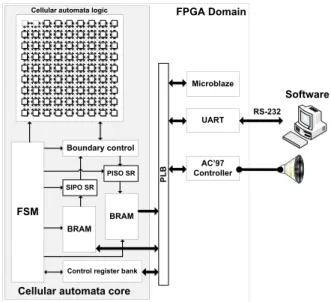
4. System architecture
The overall architecture of the system described in this work consists of a digital system design for a FPGA device and software desktop application, which is a graphical tool for the system user that provides an interface to control the hardware operation, a representation of the CA to initialize and read its state map, and the generation of bitstream files each one equivalent to a single custom CA specification. Thus, our approach allows the system user to parameter-ize the hardware architecture according to its needs. Pre-built templates, that describe in Verilog the circuits of sep-arate modules, are used as a reference to integrate complete CA specifications in the design. The CA characteristics are template configuration parameters, i.e. lattice dimensions, neighbourhood type and number of bits per cell, and the state evolution rule is the body of the cell modules that de-termine its functionality.
Currently, the architecture of the hardware system is flexible enough to support the following features: multidi-mensional lattices (1D and 2D), Moore and von Neumann neighbourhoods, periodic or null lattice boundary condi-tions and unconstrained number of state resolution bits per cell; the lattice width is, however, constrained to multiples of 8. The state evolution rule can be specified with logical and arithmetic operations at the bit level. Furthermore, it is
Boundary control
FSM BRAM
BRAM
Control register bank
Microblaze
UART
AC’97 Controller
FPGA Domain
Cellular automata logic
SIPO SR PISO SR
Cellular automata core
RS-232
Software
PLB
Figure 1. System architecture
also possible to provide different rules to different rows of cells in the lattice, which is an advantage to simulate mul-tiple 1D CAs in parallel. Two operation modes are sup-ported: run-through for n iterations or step-by-step.
4.1. Hardware specification
4.1.1. Global architecture
The overall hardware architecture is shown in figure 1. The FPGA domain it is further divided in two distinct sub-systems: the CA core and the soft-core processor MicroB-laze. The MicroBlaze is used to transfer via RS-232 the cells state data, by accessing data stored in BRAM in the CA core, from and to the host software application and im-plements a simple protocol to do so. Moreover, the audio codec AC’97 is used for demonstration purposes to gen-erate melodies according to the state map of the CA. The melody generator function receives the state data of a row of cells and determines the bit density, i.e. the number of bits equal to 1 over the total number of cell bits in the row. The function output is the note frequency to be played gen-erating a square wave. This frequency is as high as the bit density; on a typical piano setup (88 keys), 100 % bit den-sity is equivalent to approximately 4 kHz.
Our development platform, the Atlys board from Dig-ilent, has, in addition to the Spartan-6 FPGA, numerous peripherals, including the audio codec chip that is used as a sound output. The hardware controllers for the audio codec and the UART are provided by Digilent and Xilinx, re-spectively; both already implement an interface to the PLB (bus). For simplicity, the corresponding available software drivers were used with the MicroBlaze CPU.
4.1.2. CA core architecture
The CA core is our custom hardware and contains the necessary modules to control the CA operation, initialize, read and hold its current state. The CA logic module
con-tains all the generated cells for a custom specification and it is not run-time configurable, i.e., it not possible to change the CA characteristics, structure or rules. Thus, every sin-gle specification is final until a newer one is provided and its corresponding bitstream generated.
Every single row of cells is generated independently as each one is constructed from a different Verilog module. Even though the top-level description and reference logic of every single cell is identical, for each row of cells the functionality is not necessarily the same, as mentioned in the architecture features. However, all the cells in the lat-tice are interconnected with each other and the number of interconnects of each cell depends on the neighbourhood type: 4 for von Neumann and 8 for Moore types. The inter-connects are buses whose width is defined by the number of bits per cell. Therefore, a single cell can have 4 or 8 inputs and always one output to pass its state to its neighbours. In case of 1D CA, each cell always has 4 inputs. The cell architecture is described in detail in section 4.1.3.
To initialize and read the state of the CA, as well as to pass cell data from one boundary to the opposite bound-ary, input (IB) and output (OB) external buses, connected to the cells on the edge of the lattice, exist. Each bus has a different width, regardless of the number of bits per cell, and it may only depend on the neighbourhood type and lat-tice structure. Each bus is indexed b by b bits, from IB and OB, forming a neighbour boundary interconnect that corre-spond to the state data of different cells along it. For exam-ple, in a 2D scenario with a von Neumann neighbourhood each boundary cell has one boundary interconnect, except the corner cells that require two. On the other hand, for a Moore neighbourhood each boundary cell has three bound-ary interconnects but the corner cells require five. Both IB and OB are connected to each other, in case of a periodic boundary, and are redirected by the boundary control mod-ule whenever needed. For a null boundary, IB is connected to the ground. This is explained with more detail in the operation modes below.
Figure 2 shows a more detailed view of the internals of the CA core with focus on the modules interconnects, bus widths and operation modes.
The cell state data is written and read to and from two dual-port BRAMs, one used as an input memory and an-other as an output memory. A 32-bit port is used to inter-face with the PLB (bus) and a 8-bit port is used internally by the core. Two shift-register (SR) modules are used in or-der to parallelize (SIPO) chunks of c × b bits and serialize (PISO) chunks of 8 bits of cell state data to be read from and written to memory, respectively, where c is the num-ber of lattice columns and b the numnum-ber of bits per cell. The SIPO SR has an 8-bit input to read data from the in-put BRAM and a outin-put of c × b bits, which is the total width in state bits of a row of lattice cells. Each stage of the SR has a 8-bit depth and such amount of data should be shifted whenever a read from memory and a write in the SR are performed. The PISO SR has an input of c × b bits and a 8-bit output to write data to the output BRAM; the functionality and structure are identical to prior SR. The length of both SRs depends on the lattice dimensions and it
SIPO Shift-register PISO Shift-register
FSM
rule shift load shift shift load select select b x c b x c b x c BRAM BRAM enable address enable write enable 8 8 12 address 12 32 32 load_ca step start stop fetch_row perform_iter n_iter 32 load_done row_read rows_read max_iterFigure 2. Detailed view of the cellular automata core is given by (c × b)/8. Thus, the number of columns of the
lattice is constrained to multiples of 8. The reason for this is to make it easier to manipulate data transfers and organi-zation for this memory configuration and processing.
The boundary control module consists of several multi-plexers to redirect boundary data buses, the IB and the OB, depending on the CA operation mode, i.e., reading, initial-izing or iterating. In the first two modes, the lattice rows are shifted in a circular fashion, from top to bottom, as state data is read from or written to the cell’s memory and, at the same time, to the I/O memories, accordingly, via SRs. After the reading operation, the state map of the CA re-mains as it was before. In the latter mode, the multiplexers redirect the OB to the IB wrapping around the lattice and, every clock cycle, a new state for every cell in the lattice is computed. In the iteration mode, the next state is always computed until the simulation time reaches n time steps; if the step-by-step mode is active, the simulation halts af-ter every iaf-teration until further order is given to continue, however it is limited as well to n time steps. In the step-by-step mode, the state map is read every iteration overwriting the previous data that was stored in memory; in the run-through mode, the state map is only read at the end of the simulation. A finite state machine (FSM) is responsible for controlling all the core modules, register operation re-sponses and listen to user command signals from a control register bank (CRB). The bank is used to synchronize op-erations between the Microblaze and the FSM as shown in Figure 1.
4.1.3. Cell architecture
The module that describes the cell architecture is unique but it is replicated c×r times, where c and r are the number of columns and rows of the lattice, respectively. It consists of a sequential circuit to hold the cell’s state and a com-binatorial circuit that implements the state transition rule. Again, an input bus and an output bus exist to receive the neighbour cells state data and pass the next state to them, respectively. The input bus has a width of 4 × b or 8 × b bits for a Moore and von Neumann neighbourhood,
respec-tively. Each b bits are the state bits of the cells adjacent to a central one. For controlling, two additional 1-bit signals are provided and are common to every single cell. One of them enables the state transition rule (iteration mode) and the other controls the direct loading of the state data from the cell located north (reading and initializing modes). Both signals are fed to two multiplexers; when neither of them is active, the cell is idle and its state remains as it is.
4.2. Software specification
The software application was written in Java, provides a simple and friendly GUI and acts as the front-end to the user of the hardware system with a high-level of abstrac-tion of technical details. This tool is capable of running a typical FPGA Design Flow to produce a bitstream file equivalent to the custom CA specification. This process is automatic and transparent to user as it occurs in back-ground by executing existing scripts. Each bitstream file is saved in a separate directory; an existing bitstream can be programmed any time. However, the current version of the tool, besides providing the features mentioned in section 4, can only generate bitstream files for a Spartan6 as the ref-erence design was built for that FPGA device in specific. However, the number of generated bitstreams is unlimited. The GUI of the software tool is shown in figure 3. The characteristics of the CA can be specified by filling in the text fields with the desired values and check box marks. On the other hand, the state transition rule must be described textually with Verilog HDL and two text areas are used for this purpose. The main one is used to explicitly indicate the state register update rule of a cell, and the other one is provided for additional optional supporting logic. To avoid knowing the input and output buses names from the Verilog module, the tool provides a simple set of tags that allow to reference quickly b bits of any neighbour interconnect. Upon saving the specification, each tag string that is found is replaced by its interconnect reference in the module de-scription, and the specification is integrated in a copy of the pre-built cell template module file located in the work-ing directory. This copy is then included in the directory
Figure 3. Graphical user interface of the software tool where all the system module files are kept; each one of
these files describe the functionality of a row of lattice cells. As for the CA characteristics, these are saved directly in the header files that are included in the core modules.
The serial communication parameters that are config-urable are the COM port and the baudrate. However, the baudrate is fixed in the design at 460800 bps which is lim-ited by the UART controller. A set of buttons in the GUI allow to interact with the FPGA once a connection is estab-lished. These buttons call functions that implement the op-erations modes and the protocol defined, that the Microb-laze implements as well, to send commands, transmit and receive cell’s state data.
To initialize and represent the state map of the CA, a graphical editor that maps cell states to colours, accord-ing to a custom palette, is provided. This utility is capable of representing a lattice with a dimension up to 200×200 cells, which is the maximum supported by the zooming function. Given that the representation area was chosen to be limited, a dragging capability was added. In addi-tion to that, the editor supports a fast paint mode that al-lows switch a cell state quickly by just dragging the mouse over the selected area instead of clicking. Nevertheless, to change a cell state with the fast paint mode disabled re-quires a click. For easier navigation when dragging the lattice, the coordinates of the cell pointed by the cursor are indicated aside. Finally, a custom palette builder enabled the representation of any given state with a RBG-specified colour; colour palettes can be saved for future use.
5. Results
5.1. Implementation and benchmarking
The architecture was implemented on a Xilinx Spartan-6 (XC6SLX45) FPGA running at 66 MHz. For initial bench-marking, we used the Game of Life algorithm which is a bidimensional CA model to simulate life. Each cell is ei-ther dead or alive, ei-therefore a single bit is required to repre-sent the state; a cell that is alive remains so if either two or three neighbours are alive as well; a dead cell with exactly three neighbours alive is born; otherwise, the cell state re-mains unchanged. A Moore neighbourhood with a periodic
boundary condition is used.
Tables 1 and 2 show the running times on several lat-tices for two different numbers of iteration. Iteration char-acteristics are summarized in tables 3 and 4. The hardware simulation time is given by tHW =n/ fCLK, where n is the
number of iterations and fCLK the clock frequency, which
is the equal to the effective computation time, tc.
The implementation results refer to the Post-PAR imple-mentation which means that the presented values are not an estimation. The percentage of the resources occupied in-clude not only our custom CA core, but the Microblaze and the UART controller as well; the audio codec controller is not included in these implementation results as it is an ex-tra feature. The computer has an Intel Core 2 Quad Q9400 running at 2.66 GHz and the software application is XLife [15]. Results show that the simulation time on hardware does not depend on the lattice size, but only on clock fre-quency (which depends on cell complexity).
We have also evaluated implementations of simplified versions of the Greenberg-Hastings CA [6] (without ran-dom event generator) and of the lattice gas model CA [7]. The results are presented in tables 5 and6, and tables 7 and8], respectively. Both rules require 4 bits per cell, how-ever the neighbourhood types are different; the GHCA uses a Moore one and the LGCA uses a von Neumann one.
From the results shown in tables 1 and 2, we can see that both exhibit almost constant speed-ups for different ar-ray sizes; although not shown here, the same behaviour was observed for a lower n. Thus, we obtain a linear relation-ship between speed-up and array size. Also note that the hardware simulation time is constant regardless of the di-mensions, which results from using just of a single clock cycle per iteration.
5.2. Data transfer time analysis
The results of subsection 5.1 related to hardware simu-lation time only take into account the CA computation time (when the CA is iterating). In order to provide a more ac-curate and fair comparison as far as benchmark goes, in this subsection we present a detailed analysis on how data transfer times impact the obtained speed-up figures. We are now going to consider not only the computation time (tc),
Benchmark — n = 108iterations
Lattice HW (s) SW (s) speed-up 32 × 32 1.5 59.2 39 40 × 40 1.5 110.8 74 56 × 56 1.5 251.8 168
Table 1. Benchmark results for Game of Life per-forming 108iterations. Benchmark — n = 109iterations Lattice HW (s) SW (s) speed-up 32 × 32 15.0 590.7 39 40 × 40 15.0 1103.5 74 56 × 56 15.0 2490.9 166
Table 2. Benchmark results for Game of Life per-forming 109iterations. Implementation Lattice FF (27,288) LUT (54,576) 32 × 32 3,083(5.6%) 10,114(37.1%) 40 × 40 3,685(6.8%) 18,449(67.6%) 56 × 56 5,243(9.6%) 24,818(90.9%) Table 3. Implementation results for Game of Life — FPGA resources occupied
Implementation Lattice Frequency (MHz) 32 × 32 85.7 40 × 40 72.8 56 × 56 69.3
Table 4. Implementation results for Game of Life — maximum frequency Implementation Lattice FF (27,288) LUT (54,576) 24 × 24 4,503(8.3%) 10,558(38.7%) 32 × 32 6,366(11.7%) 17,071(62.6%) 40 × 40 8,717(16.0%) 23,854(87.6%) Table 5. Implementation results for Greenberg-Hastings CA — FPGA resources occupied
Implementation Lattice Frequency (MHz) 24 × 24 71.4 32 × 32 68.7 40 × 40 69.2
Table 6. Implementation results for Greenberg-Hastings CA — maximum frequency
Implementation
Lattice FF (27,288) LUT (54,576) 56 × 56 14,989(27.5%) 15,394(56.4%) 64 × 64 18,894(34.6%) 19,295(70.8%) 72 × 72 23,311(42.7%) 23,870(87.5%) Table 7. Implementation results for lattice gases CA — FPGA resources occupied
Implementation Lattice Frequency (MHz) 56 × 56 76.7 64 × 64 69.4 72 × 72 77.2
Table 8. Implementation results for lattice gases CA — maximum frequency
r × c TB(ms) 24×24 1.25 32×32 2.22 40×40 3.47 48×48 5.00 56×56 6.81 64×64 8.89 72×72 11.25
Table 9. Time required to transfer cell data for b = 1 but also a) the time it takes to write (CMw) and read (CMr)
data from the CA array of flip-flops to and from the mem-ory, and b) the time it takes to transfer the initialization data from the PC to the FPGA (tsi) and read the results back to
the PC (tso). Other existing overheads are also exposed.
It was mentioned in section 4.1 that data is transferred via RS-232 protocol and serial interface, with a baudrate of B = 460800 bps limited by the provided controller. The amount of data to transfer, regardless of initializing or read-ing results back, is always the same given a certain CA specification. Given that each cell contains b bits of data distributed in a lattice of c columns and r rows, the time it takes to transfer the data is given by
TB=tsi=tso =r × c × bB (1)
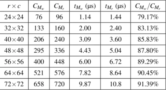
Table 9 summarizes the time length to transfer data for some lattice dimensions. All the data that is written to and read from memories is held, for a certain amount of time, in the shift-registers (SR) whose structure and functional-ity was described in section 4.1. Shifting cells data is re-quired whenever a new state is to be loaded or the current state read from the array; such operations take time which is worse for larger lattice dimensions and increasing num-ber of bits of cells state data.
The time it takes to load and read the CA array, CMwand
CMr, respectively, are not equal for two reasons. The first
is that when reading data from memory there is always one clock cycle of latency; the second is that the clock cycle to load data to the first stage of the SIPO SR is the same when a new row is loaded to the CA array, which means both op-erations occur in parallel saving up one clock cycle; in fact, more than one clock cycle is saved up, as it is explained below, which determines that effectively CMw≤ CMr. To
determine the expression of CMw, given in clock cycles,
we consider two different situations: when the SIPO SR is fully loaded for the first time, whenever a initialization operation begins, and then the subsequent loads. Then,
CMw=1 +c × b8 +r + r ·! c×b8 −1
"
(2) The first two terms refer to the first load: a clock cycle of latency only taken into account once and then filling and shifting (c×b)/8 stages of data of SIPO SR. The remaining two terms refer to the subsequent SR loads: the first stage
is loaded r times as well as r rows are loaded into the CA array, which saves up r clock cycles; the last term accounts for the loading of the remaining stages also occurring for r times. Simplifying the expression, we obtain
CMw=1 +c × b8 ·(r + 1) (3)
The expression of CMr is simpler to determine. When
read-ing the CA array, it is shifted for an amount equal to the number of lattice rows, r, as well as to load a rows to the PISO SR. Then, the PISO SR shifts data to be written to the memory, a number of times equal to the number of stages available, again, r times. As a downside, for this case, it is required that all the data present in the SR is shifted out be-fore loading up another row, in order to avoid loss of data, which consumes more time. So,
CMr=r · ! 1 +c × b 8 " (4) To obtain the effective time tMwand tMr, given in time units
and not clock cycles, we simply divide expressions 3 and 4 by fCLK, the clock frequency.
Table 10 summarizes the time length to load and read the CA array for some lattice dimensions. We can observe that as the lattice dimensions become larger, the time to load the CA array tends to approximate to the time required to read it. This is obvious if we think that the gain of r clock cycles mentioned above becomes irrelevant as r × c grows. In fact, when r,c → ∞ we obtain from expressions 4 and 3
CM=CMw=CMr≈r × c × b8 . (5)
As we are interested in generating the largest lattices possi-ble, we can use expression 5 to the determine a good ap-proximation to the effective speed-up. From the results presented on table 10, for a squared lattice, we can also conclude that the time grows quadratically with (b/8) · x2,
where x is the side of the lattice. For a non-squared lat-tice, the time grows linearly with the rows or columns. The quadric behaviour shows whenever r → c or vice-versa.
As a final remark to this matter, we point out that there are still two existing overheads on the side of the hardware and software that were not measured accurately. From the hardware side, a small amount of time is required to read data from memory and write them to the serial buffer; this is about the same time it takes to read data from the se-rial buffer and write them to the memory. From the soft-ware side, it is necessary to consider the time to read the data from the graphical display buffer and write it to the se-rial buffer and vice-versa. Even though data is represented graphically as it is received, we believe that the software overhead is longer. However, we are able to safely con-clude that the data transfer over the serial interface is the bottleneck.
The effective speed-up is determined solely by the lat-tice dimensions and cell state data bits; it does not depend on the present rule. Adding the computation time tcto the
expressions 1 and 5 we obtain the expression for the effec-tive hardware simulation time for a single experiment, i.e.,
r × c CMw CMr tMw(µs) tMr(µs) CMw/CMr 24×24 76 96 1.14 1.44 79.17% 32×32 133 160 2.00 2.40 83.13% 40×40 206 240 3.09 3.60 85.83% 48×48 295 336 4.43 5.04 87.80% 56×56 400 448 6.00 6.72 89.29% 64×64 521 576 7.82 8.64 90.45% 72×72 658 720 9.87 10.8 91.39%
Table 10. Time required to load and read the CA array, reading and writing data to memory, with b = 1 initialize the array, iterate n times and read the results back to the PC (hence the multiplication by 2):
tHWe f f ≈ n fCLK +2 · (r × c × b) · ! 1 B+ 1 8 · fCLK " (6) where n is the number of iterations. Using expression 6 and the results from tables 1 and 2, we can now determine the percent reduction of the speed-up, ps. Considering a
lattice size of 56×56, for 108and 109iterations we obtain
a reduction of about 0.9% and 0.09%, respectively. For a lattice size of 40×40 we obtain a reduction of about 0.46% and 0.046%. However, as n decreases, psincreases
drasti-cally, e.g., for 105iterations the percent reduction is 90.1%
and 82.3%. This is expected because the time required to transfer data has a greater impact on a shorter computation time. Thus, the linear relationship observed in section 5.1 between speed-up and dimensionality only occurs for large values of n, where psis not significant.
6. Conclusions and Future Work
The implementation described in this work performs the evaluation of the whole CA array in parallel, and consti-tutes a fully functional and flexible system. However, some improvements can be envisioned. The synthesis and imple-mentation processes run by the associated tools are auto-matic, which means that there is no control of the mapping of the CA to the FPGA resources. It is not guaranteed that CA cells are uniformly distributed across the FPGA, which leads to the degradation of performance and a lower de-gree of compactness—there is a waste of resources as the cells are spread irregularly and their neighbourhood inter-connections have different lengths.
The major advantages of CA architectures are its lo-cal connectivity and spacial regularity, which allow excep-tional performance on hardware. In future, solutions to op-timize distribution and allocation of FPGA resources need to be investigated, for example, at the floorplanning level. Moving on to a multi-FPGA scenario with greater capacity, based, for instance, on Virtex-6 devices, would enable the support of larger lattices.
Acknowledgments This work was partially funded by the European Regional Development Fund through the COMPETE
Programme (Operational Programme for Competitiveness) and by national funds from the FCT–Fundac¸˜ao para a Ciˆencia e a Tecnologia (Portuguese Foundation for Science and Technology) within project FCOMP-01-0124-FEDER-022701.
References
[1] John Von Neumann. Theory of Self-Reproducing Automata. University of Illinois Press, Champaign, IL, USA, 1966. [2] Stephen Wolfram. A New Kind of Science. Wolfram Media,
2002.
[3] V. Zhirnov, R. Cavin, G. Leeming, and K. Galatsis. An As-sessment of Integrated Digital Cellular Automata Architec-tures. Computer, 41(1):38 –44, jan. 2008.
[4] Eric W. Weisstein. Game of life. From
MathWorld–A Wolfram Web Resource.
http://mathworld.wolfram.com/GameofLife.html.
[5] M. Gardner. The fantastic combinations of John Conway’s new solitaire game “life”. Scientific American, 223:120– 123, October 1970.
[6] Nikolaos Vlassopoulos, Nazim Fates, Hugues Berry, and
Bernard Girau. An FPGA design for the stochastic
Greenberg-Hastings cellular automata. In 2010 Interna-tional Conference on High Performance Computing and Simulation (HPCS), pages 565–574, June 28 2010-July 2 2010 2010.
[7] Paul Shaw, Paul Cockshott, and Peter Barrie. Implemen-tation of lattice gases using FPGAs. The Journal of VLSI Signal Processing, 12:51–66, 1996.
[8] Stephen Wolfram. Cellular Automata And Complexity: Col-lected Papers. Westview Press, 1994.
[9] Burton H. Voorhees. Computational Analysis of
One-Dimensional Cellular Automata. World Scientific Series on Nonlinear Science. Series A, Vol 15. World Scientific, 1996.
[10] Eric W. Weisstein. Moore Neighborhood.
From MathWorld–A Wolfram Web Resource
http://mathworld.wolfram.com/ MooreNeighborhood.html.
[11] Eric W. Weisstein. von Neumann
Neighbor-hood. From MathWorld–A Wolfram Web
Re-source. http://mathworld.wolfram.com/
vonNeumannNeighborhood.html.
[12] Paul Shaw and George Milne. A highly parallel fpga-based machine and its formal verification. In Herbert Gr¨unbacher and Reiner W. Hartenstein, editors, Field-Programmable Gate Arrays: Architecture and Tools for Rapid Prototyping, volume 705 of Lecture Notes in Computer Science, pages 162–173. Springer Berlin Heidelberg, 1993.
[13] Tommaso Toffoli and Norman Margolus. Cellular automata machines: a new environment for modeling. MIT Press, Cambridge, MA, USA, 1987.
[14] Tommaso Toffoli and Norman Margolus. Cellular automata machines. Complex Systems, 1(5):967–993, 1987.
[15] Jon Bennett, Chuck Silvers, Paul Callahan, Eric S. Ray-mond, and Vladimir Lidovski (2011-2012). XLife. http: //litwr2.atspace.eu/xlife.php.