Mestrado Integrado em Engenharia Biomédica
Ramo de Eletrónica Médica
Trabalho efetuado sob orientação do:
Professor Doutor Paulo Mateus Mendes
Sofia Daniela Sousa Gomes
CMOS Receiver for Wireless Powering of
Implantable Biodevices
Universidade do Minho
DECLARAÇÃO
Nome: Sofia Daniela Sousa Gomes
Endereço Eletrónico: gomessds@gmail.com Telefone: +351 911 894 620
Número do Bilhete de Identidade: 13906563
Título dissertação: CMOS receiver for wireless powering of implantable biodevices Orientador: Professor Doutor Paulo Mateus Mendes
Ano de conclusão: 2014
Designação do Mestrado: Mestrado Integrado em Engenharia Biomédica Área de Especialização: Eletrónica Médica
É AUTORIZADA A REPRODUÇÃO INTEGRAL DESTA TESE APENAS PARA EFEITOS DE INVESTIGAÇÃO, MEDIANTE DECLARAÇÃO ESCRITA DO INTERESSADO, QUE A TAL SE COMPROMETE.
Universidade do Minho, ____/____/________
Assinatura: ______________________________________________________
A
CKNOWLEDGMENTS
Firstly, I wish to express my most sincere gratitude to my parents for their love, patience, unconditional support, encouragement and absolute dedication given throughout my life. The success throughout my life would have not been possible without their guidance.
A very special thanks to my supervisor Professor Paulo Mendes for the support, experience, advice and for the encouragement to overcome all problems and challenges that came across during my work. I also wish to thank for the opportunity to work on the scientific project sponsored by PTDC/EEI-TEL/2881/2012, Programa Operacional Temático Fatores de Competitividade (COMPETE) and Fundo Comunitário Europeu FEDER.
Finally, I want to thank my dear friends for their friendship, patience, support, affection and, most importantly, for the entertaining moments. I wish to thank, in particular, David Barbosa for all the patience, dedication and encouragement given, during this work.
A
BSTRACT
Currently, wireless biomedical devices are indispensable in healthcare, due to their various possible applications, such as physiological parameters monitoring, aiding in diagnosis and assisting in therapies, and the complement or replacement of biological functions. Therefore, exploring ways to prolong their lifetime is imperative, since this allows avoiding invasive surgical procedures to substitute the devices. One way of prolonging the lifespan of these devices is to harvest energy from the ambient or from a dedicated source and use it to charge their batteries. Radiofrequency (RF) energy is suitable for long distance energy transportation and is the basis of all telecommunication systems. Thus, it is available practically everywhere. In addition, its absorption by body tissues, as long as the established limits are not exceeded, does not present significant secondary effects in health.
The major purpose of this work is the design of a CMOS system to power wireless implantable biodevices, capable of collecting RF energy, when combined with an antenna, and using it as an energy source to power a battery charging circuit and charge a storage element.
Prior to the implementation of the CMOS system, an approach using off-the-shelf components was elaborated on a PCB to determine and analyze the testing conditions to which the first would be exposed. To assess the conversion ability of the PCB rectifier, a 1 kΩ resistive load was added in series to calculate the output DC power by measuring the voltage across it. The suitability of this circuit for wireless power transfer (WPT) was assessed to know and define the conditions and setup to test the CMOS circuit for this energy transfer process. In addition, it allowed to more accurately simulate the behavior and operation of the CMOS system. As proof that energy transfer and conversion occurred, a LED was added to the output of the rectifier with the purpose of turning on when sufficient energy was converted. This system was intended to power a commercial battery charging circuit and charge a supercapacitor, using the WPT setup.
The simulations regarding the operation of the CMOS system showed it should be capable of charging a storage element. Different resistive loads were added in parallel to the storage element, in order to mimic the operation of the charging system, when it is powering other circuits. Even though the storage element is charged, it is not charged up to the maximum voltage possible, thus, a battery management system should be added in the future.
R
ESUMO
Atualmente, os dispositivos biomédicos sem-fios são indispensáveis na área da saúde, devido às diversas aplicações possíveis, tais como a monitorização de parâmetros fisiológicos, a assistência no diagnóstico e em terapias, e no complemento ou substituição de funções biológicas. Assim, a procura de formas para prolongar o tempo de vida destes dispositivos é imperativa, uma vez que, assim, são evitados procedimentos cirúrgicos invasivos para a substituição dos mesmos. Uma forma de prolongar o tempo de vida destes é através da recolha de energia existente no meio ambiente, ou disponibilizada por uma fonte dedicada, e utilizá-la para carregar as baterias presentes nos mesmos. A energia de radiofrequência (RF) é adequada para o transporte de energia a longas distâncias e constitui a base de todos os sistemas de telecomunicações, estando presente praticamente em toda a parte. Para além disso, a sua absorção pelos tecidos do corpo humano, desde que não exceda os limites estabelecidos, não apresenta efeitos secundários para a saúde.
O objetivo deste trabalho é a conceção de um sistema CMOS para carregamento de biodispositivos implantáveis e sem-fios, capaz de recolher energia de RF, quando combinado com uma antena, e usá-la como fonte de energia para alimentar um circuito de carregamento de baterias.
Antes de implementar o dispositivo em tecnologia CMOS, desenvolveu-se uma abordagem usando componentes comerciais numa placa de circuito impresso para determinar as condições de teste às quais o primeiro estará sujeito. De forma a analisar a capacidade de conversão deste circuito, foi adicionada uma carga de 1 kΩ ao mesmo para calcular a potência de saída DC, através da medição da queda de tensão aos terminais da carga. A adequabilidade deste circuito para transferência de potência sem-fios foi determinada de modo a definir as condições e o equipamento para testar o circuito CMOS, para o mesmo processo. Isto permitiu, ainda, simular de forma mais correta e precisa o comportamento do sistema CMOS. Para provar que ocorreu transferência e conversão de energia, um LED foi adicionado à saída do retificador, sendo ligado quando energia suficiente é convertida. Pretendia-se que este sistema alimentasse um carregador de baterias comercial para carregar um supercondensador, através de transferência de energia sem-fios.
As simulações relativas ao funcionamento do sistema CMOS mostraram que este deverá ser capaz de carregar uma bateria. Diferentes cargas resistivas foram adicionadas em paralelo
vi
ao supercondensador, de forma a replicar o funcionamento do sistema quando este alimenta outros circuitos. Apesar do supercondensador ser carregado, este não carrega até à tensão máxima disponível, assim, um sistema para gestão do uso bateria deverá ser adicionado.
C
ONTENTS
Acknowledgments ... i
Abstract... iii
Resumo ...v
List of Figures ... ix
List of Terms ... xiii
Chapter 1 – Introduction...1
1.1 Wireless biomedical devices ...1
1.1.1 Wireless device powering ...2
1.1.2 Energy harvesting ...2
1.2 Motivation and aim of the dissertation ...3
1.3 Contributions ...4
1.4 Outline and structure ...4
Chapter 2 – RF energy harvesting ...7
2.1 Wireless power transfer ...8
2.1.1 Free-space path loss...8
2.1.2 Frequency selection for WPT ...9
2.1.3 RF-DC converter ...9
2.2 Rectifying systems on-chip ... 11
2.2.1 External-Vth-cancelation technique ... 12 2.2.2 Internal-Vth-cancelation technique ... 13 2.2.3 Self-Vth-cancelation technique ... 14 2.2.4 Differential rectifier ... 14 2.3 Rectifying system on PCB ... 16 2.3.1 Bridge topology ... 16
2.3.2 Double voltage topology ... 17
2.3.3 Double current topology ... 18
2.3.4 Single-series topology ... 19
Chapter 3 – PCB RF-DC converter design ... 21
3.1 Board design ... 21
3.2 Rectifying circuit operation ... 25
viii
3.3.1 Rectifying circuit ... 29
3.3.2 Battery charging circuit ... 29
Chapter 4 – On-chip RF-DC converter design ... 35
4.1 Rectifier operation ... 35
4.2 Battery charger operation ... 39
Chapter 5 – Tests and results ... 45
5.1 PCB RF-DC converter ... 45
5.1.1 Power conversion efficiency ... 46
5.1.2 Wireless power transfer ... 48
5.1.3 Battery charging system ... 53
5.2 On-chip RF-DC converter ... 53
5.2.1 Charging system operation ... 53
5.2.2 RFCMOS testing protocol ... 56
Chapter 6 – Conclusions and future work ... 63
6.1 Conclusions ... 63
6.2 Future work ... 65
Bibliography ... 67
Appendices ... 73
L
IST OF
F
IGURES
Figure 2.1 – Schematic of a RF-DC rectifier block, where Vin is the RF input signal source, Rin
is the source’s internal resistance and Rout is the output load. ... 10
Figure 2.2 – Conventional CMOS rectifier using NMOS transistors... 12
Figure 2.3 – NMOS rectifier using EVC technique to compensate the Vth. ... 13
Figure 2.4 – Rectifier using IVC technique to compensate the Vth. ... 13
Figure 2.5 – SVC rectifier configuration. ... 14
Figure 2.6 – SVC differential rectifier topology. Transistors N1 and P1 comprise the MOS pair 1 and N2 and P2 comprise the opposite MOS pair 2. ... 15
Figure 2.7 – Circuit equivalent to the SVC differential rectifier topology presented in Figure 2.6. ... 15
Figure 2.8 – (a) Bridge RF rectifier topology. (b) Current pathway when diodes D1 and D2 are turned on, and diodes D3 and D4 are turned off. (c) Current pathway when diodes D1 and D2 are turned off, and diodes D3 and D4 are turned on. ... 17
Figure 2.9 – (a) Greinacher double-voltage rectifying circuit, and its behavior during (b) the negative half cycle and (c) the positive half cycle. ... 18
Figure 2.10 – Full-wave voltage quadrupler. ... 18
Figure 2.11 – Double-current rectifying circuit. ... 19
Figure 2.12 – Single-series diode topology. ... 19
Figure 3.1 – Cross-section of a coplanar waveguide transmission line. ... 21
Figure 3.2 – (a) Transmission line, (b) gap dimensions and (c) short-circuit dimensions used for design simulations, printed on a 5x5cm board made of Arlon-Med 60 mil AD250A substrate (not drawn to scale). ... 23
Figure 3.3 – Simulated and measured (a) S11 and (b) S21 parameters (in dB) of the transmission line printed on the 60 mil AD250A substrate, for frequencies between 1 GHz and 4 GHz. .... 24
Figure 3.4 – Schematic of the rectifying circuit composed of a 1 µH inductor, a Schottky diode and a 1.2 pF capacitor. ... 25
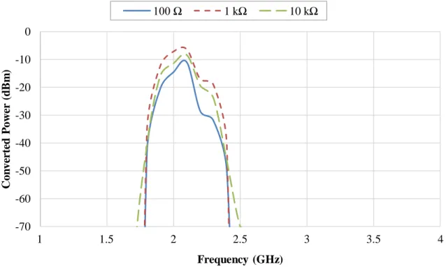
Figure 3.5 – Converted output DC power (in dBm) obtained with 100 Ω, 1 kΩ and 10 kΩ output loads, for frequencies between 1 GHz and 4 GHz and 0 dBm input power. ... 26
x
Figure 3.7 – System used to simulate the S11 parameter of the implemented PCB, evidencing
the distances between components and the dimensions of the CPW (not drawn to scale). ... 27
Figure 3.8 – Measured (for 0 dBm, 5 dBm, 10 dBm and 15 dBm input powers) and simulated (0 dBm input power) S11 parameter (in dB) of the implemented rectifier with a 1 kΩ load, for frequencies ranging from 1 GHz to 4 GHz. ... 28
Figure 3.9 – Schematic of the battery charging system. ... 28
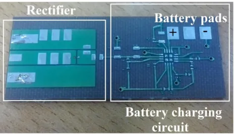
Figure 3.10 – Board designed for the rectifier and the battery charging circuit. ... 29
Figure 3.11 – Low-power battery charging circuit. ... 30
Figure 3.12 – Different voltages and operation modes of the device [55]. ... 32
Figure 4.1 – SVC differential rectifier topology. ... 36
Figure 4.2 – Three-stage SVC rectifier configuration. MOS devices Nx,1 and Px,1 comprise pair 1 and Nx,2 and Px,2 are the opposite pair 2 of stage x. ... 37
Figure 4.3 – Output DC voltages (in mV) at various loads (500 kΩ, 1 MΩ, 5 MΩ, 10 MΩ and open-circuit), for input voltages between 100 mV and 1000 mV, with a 100 mV step size and input frequencies (a) 1 GHz, (b) 1.5 GHz, (c) 2 GHz, (d) 2.5 GHz, (e) 3 GHz, (f) 3.5 GHz and (g) 4 GHz. ... 38
Figure 4.4 – Operational transconductance amplifier... 40
Figure 4.5 – Current-gain stage. ... 40
Figure 4.6 – End-of-charge detector. ... 41
Figure 4.7 – NMOS current mirror with a resistor setting the reference current IREF. ... 41
Figure 4.8 – (a) Voltage at the supercapacitor for 500 mV and 1000 mV supply voltages at the beginning of the charging. End-of-charge output flag transition from ground to the supply voltage, indicating the end of the charging process for (b) 500 mV and (c) 1000 mV supply voltages. ... 44
Figure 5.1 – Setup for determining the efficiency of the RF to DC conversion. The VNA synthesizes the RF signal, which is rectified by the proposed circuit, and the output DC voltage is measured by adding a resistive load. ... 46
Figure 5.2 – Converted DC output power (in dBm) at the 1 kΩ load, for 0 dBm, 5 dBm, 10 dBm and 15 dBm RF input powers and frequencies between 1 GHz and 4 GHz. ... 47
Figure 5.3 – PCE (in %) of the rectifying circuit with the 1 kΩ load, for 0 dBm, 5 dBm, 10 dBm and 15 dBm RF input powers and frequencies between 1 GHz and 4 GHz. ... 47
Figure 5.4 – Microantenna used in the experiments, soldered to (a) a board (used in the first
in later experiments immersed in aqueous solution). In (c), the 3D structure of the antenna is
emphasized. ... 49
Figure 5.5 – (a) Wireless power transfer measurement setup main components: a VNA serves as the RF signal source, which is amplified and, then, emitted by a horn antenna. The microantenna acts as the RF signal receiver and the energy is transferred to the rectifying circuit, which converts the alternating signal to DC current. A resistive load is once again used to determine the output DC power. (b) Setup used in WPT, emphasizing each component. ... 50
Figure 5.6 – S11 parameter (in dB) of the 3D microantenna immersed in water, for frequencies ranging from 1 GHz to 4 GHz... 51
Figure 5.7 – Received DC output power (in dBm) at the 1 kΩ load, for 0 dBm, 5 dBm, 10 dBm and 15 dBm RF input powers (at the end of the signal generator and input of the amplifier), for frequencies between 1 GHz and 4 GHz. ... 52
Figure 5.8 – Close-up of the rectifying circuit exhibiting the LED turned on by WPT. The size of the components is compared to a 1 cent coin. ... 52
Figure 5.9 – (a) CMOS rectifier and (b) CMOS battery charger. ... 54
Figure 5.10 – Voltages (in mV) at the output of the rectifier (VDC) and at the supercapacitor (VCap), for RF input amplitude voltages between 500 mV and 1000 mV, with a 100 mV step size, at 2 GHz. ... 55
Figure 5.11 – Comparison between the supply voltage and the voltage at the supercapacitor (in mV), for RF input amplitude voltages between 500 mV and 1000 mV, with a 100 mV step size, at 2 GHz, when a resistive load (1 kΩ, 10 kΩ, 100kΩ or 1 MΩ) is added in parallel to the supercapacitor. ... 56
Figure 5.12 – (a) Circuit used to test situation 1, evidencing the input, output and ground pads. (b) Close-up of the rectifier. ... 58
Figure 5.13 – Pads arranged in the GSG configuration, with a guard ring in metal 1. ... 59
Figure 5.14 – (a) Circuit used to test situation 2, evidencing the required pads. (b) Close-up of the battery charging circuit. ... 59
Figure 5.15 – Circuit used to test situation 3, evidencing the required pads. ... 60
Figure 5.16 – Circuit used for testing situation 4, evidencing the required pads. ... 61
L
IST OF
T
ERMS
AC Alternating current
CMOS Complementary metal-oxide-semiconductor
CPW Coplanar waveguide
DC Direct current
EM Electromagnetic
EVC External-Vth-cancellation
FSPL Free-space path loss
IC Integrated circuit
IVC Internal-Vth-cancellation
LED Light-emitting diode
MOSFET Metal oxide semiconductor field effect transistor
MPPT Maximum power point tracking
MRI Magnetic resonance imaging
OTA Operational transconductance amplifier
PCE Power conversion efficiency
RF Radiofrequency
SAR Specific absorption rate
SVC Self-Vth-cancellation
Tanh Hyperbolic tangent
VNA Vector network analyser
Vth Threshold voltage
C
HAPTER
1
–
I
NTRODUCTION
Nowadays, wireless biomedical instruments and sensors play an essential role in healthcare, having various applications ranging from monitoring physiological parameters, aiding in diagnosis and assisting in therapies, to the complement or replacement of biological functions [1]. Despite all these benefits, it was only until recent decades that wireless devices started to be employed in the medical field, since not all requirements regarding reliability or performance were met, or the fabrication of these devices was quite expensive [2]. The advances in integrated circuit technology and wireless communications have brought more wireless healthcare solutions, assisting in the employment of new therapies or means for diagnose, when the wired alternatives are generally unsafe or uncomfortable for the patient or even impossible to be employed in some situations [2], [3].
1.1 Wireless biomedical devices
Several wireless medical solutions are available for a vast range of applications. These solutions include wireless capsule endoscopy, which is swallowed by the patient in order to evaluate the whole gastric track, including the small bowel that is not accessible by conventional endoscopy [4]; implantable retinal prosthesis for the recovery of visual sensation of blind patients [5]; cardiac pacemakers to compensate slow cardiac rhythms [6]; implantable neurological stimulators for the treatment of diseases such as Parkinson’s disease, Essential Tremor and Dystonia [7].
Moreover, the advances and progress in biomedical devices occur in such an accelerated pace that, nowadays, methods for the navigation of microdevices through body fluids are even under investigation. Controlled navigation of microdevices through the human body enables the access of remote locations unreachable by current minimally invasive medical instruments, thus, allowing the emergence of new procedures and treatments, in the future. Examples of the possible procedures include minimally invasive surgeries such as reopening of blocked or clogged blood vases, controlled and highly localized drug delivery systems for chemotherapy, thermal treatment of tumors using magnetic modulation in particular regions, MRI image
Chapter 1 – Introduction
2
contrast agents for early detection in pre-selected areas, carriers and microsensors to monitor biological signals and properties, in vivo molecular MRI imaging by using magnetic nanoparticles at selected sites, diagnostic tools to measure various properties at pre-selected sites, minimally invasive procedures, novel methods to treat aneurysm, and many more [8]– [10]. Wireless microdevices specifically designed for a particular task, which can navigate within the human body, present many benefits concerning the access of remote areas comparing with the existing medical tools [10].
1.1.1 Wireless device powering
The proper functionality of medical devices relies on the supply of a sufficient amount of energy and their autonomy is usually restricted by the duration and size of the battery (as, presently, all portable devices are battery-powered [11]), which influences the dimensions, lifetime and potential of the device [1], [3]. Therefore, a trade-off between size and autonomy is required. Nevertheless, the energy source of a medical device must fulfil certain specifications, namely reliability and predictability of performance, in order to ensure the safety of the patients; and ought to be capable of continuously delivering a sufficient amount of energy to the device. Should there be any malfunction in the operation of the device, it may cause undesired effects or damage to the patient, or even death. Moreover, the source must not present undesired effects to the human body, as it should not be poisonous, damage tissues or disturb vital signals and activities [1].
Contrary to external devices, which have more available space, and hence higher design flexibility, implantable or invasive ones have several restrictions regarding size due to the limited available space inside the human body and the target location. Thus, the substitution of the device is impractical and should be avoided, as well as, any adjustments to it, as surgical procedures may be required [1], [3], [12].
1.1.2 Energy harvesting
Ambient energy harvesting or the use of a dedicated external source are plausible alternatives in powering low-power electronic devices. Energy harvesting is a rather appealing approach due to its potential as an inexhaustible energy source [13]. Nevertheless, both allow the continuous powering of these devices, which would enable them to be batteryless [14]. On
Chapter 1 – Introduction
the other hand, since batteries have charging profiles which allow to prolong their lifetime [6], battery powered devices may be charged so that this characteristic is maximized [14].
There are several sources that can be used to power or recharge low-power devices: motion or vibration, thermoelectric, magnetic induction, electromagnetic (EM) radiation, among others [1]. Electromagnetic radiation, particularly radiofrequency (RF), is suitable for long distance energy transportation and is accessible almost everywhere: all telecommunication systems resort to RF energy transmission (AM and FM radio, television broadcasting systems, mobile phone networks, WiFi etc. [15], [16]) [1], [17]. Moreover, its absorption by body tissues, as long as it does not exceed the established limits, does not present significant effects for one’s health [18]. Therefore, RF radiation is a reasonable choice for an energy source.
The process of transmitting RF energy through space and collecting it by a receiver is known as wireless power transmission (WPT). Usually, in biomedical applications, the transmitting end is external and is placed outside the human body, whereas, the receiving end is placed inside the human body or at its surface [19].
1.2 Motivation and aim of the dissertation
As mentioned above, wireless devices may provide many benefits in the medical field and novel solutions to replace batteries in powering these devices are required, in order to avoid their substitution resorting to invasive or surgical procedures, which are uncomfortable to the patient.
In addition, the available results regarding the use of the self-folding technique lead to the conclusion that it will allow the fabrication of very small RF passives and antennas. The self-folding technique employs common microfabrication methods in order to produce microstructures with complex forms and shapes, with low costs when comparing to other methods already used [20]. This may represent an important step to an inexpensive method of integration of RF passives and antennas, without reducing system performance.
Since the use of RF energy as the energy source is rather advantageous, the purpose of this dissertation is the development of a microelectronic circuit, in CMOS technology, in order to rectify the RF signal received by a microantenna and convert it, so that it may be used to power implantable or invasive devices.
Moreover, the work developed in this dissertation was part of the scientific project PTDC/EEI-TEL/2881/2012, sponsored by the Portuguese Foundation for Science and
Chapter 1 – Introduction
4
Technology, the purpose of which is the fabrication of 3D RF microdevices using self-folding techniques. More specifically, the following objectives were considered:
1. Design and simulation of the electronic circuit;
2. Implementation of the electronic system, using off-the-shelf components; 3. Testing of the rectifier regarding power conversion and wireless power transfer;
4. Layout of the CMOS microcircuit, using the appropriate technology for RF applications;
5. Development of a protocol to test the CMOS microcircuit.
1.3 Contributions
A RF-DC rectifying circuit, which can be used for wireless power transfer, was simulated and implemented using discreet components. In addition, a CMOS microcircuit was simulated and designed to convert RF signals into DC ones and power a battery. The following publications resulted from this work:
• S. Gomes, J. Fernandes, P. Anacleto, E. Gultepe, D. Gracias, and P. M. Mendes, “Ultra-Small Energy Harvesting Microsystem for Biomedical Applications,” Proceedings of
the 44th European Microwave Conference, pp. 660-603, Rome, Italy, October 2014.
(Oral presentation).
• F. Rodrigues, S. Gomes, P. Anacleto, J. Fernandes, P. M. Mendes, "RF CMOS Wireless Implantable Microsystem for Sacral Roots Stimulation with On-Chip Antenna and Far-Field Wireless Powering", IEEE International Symposium on Circuits and Systems (ISCAS), May 24 to 27, Lisbon, Portugal. (Submited).
• P. Anacleto, S. Gomes, P. M. Mendes, E. Gultepe, D. H. Gracias, "Microcube Antennas for Efficient, Wireless Energy Transfer in Dispersive Media“. (Journal paper in preparation for Advanced Materials).
1.4 Outline and structure
The present dissertation is divided in 6 chapters, each one containing a relevant part of the work carried out, which are presented as follows.
Chapter 1 – Introduction
The present chapter describes the motivation and context of the dissertation, presenting a brief explanation of the potential advantages of using RF energy to power wireless implantable devices, as well as the objectives and contributions of this work.
Chapter 2 focuses on state of the art circuit topologies used in RF-DC conversion and describes their characteristics, operation and power efficiency conversion.
Chapter 3 describes the discreet component rectifying and battery charging circuits and the boards designed to implement these circuits.
In Chapter 4, the behavior of the designed and implemented CMOS rectifying and battery charging circuits is presented.
Chapter 5 reports and discusses the tests performed to the circuits of chapters 3 and 4 in detail and describes the setups and equipment used in the tests.
Finally, in Chapter 6, conclusions about the work are presented and possible future improvements are suggested.
2
C
HAPTER
2
–
RF
ENERGY HARVESTING
The constrained energy capacity of storage devices limits their application in miniature and implantable devices, by shortening their lifetime and requiring replacement or recharge. To overcome this limitation, several alternative energy sources have been investigated. For implantable devices with longer lifetime than the lifespan of the used storage devices, harvesting energy from the ambient for powering devices is a rather attractive due to the inherent potential to provide power indefinitely. Research in this field has grown significantly within both academic community and industry [1], [13], [21], which demonstrates that this approach is feasible, marketable and research worthy.
Nevertheless, harvesting useful amounts of energy from the environment is a rather challenging task. The quantities of available energy vary and are unpredictable and intermittent, hence, special voltage-regulating and power-management circuits are often required [1], [13]. On the other hand, the advances in integrated circuit design and fabrication techniques allow the fabrication of ultralow-power electronic devices. Regardless, removing the energy storage system is not a feasible strategy, in most cases. [22]. Being a crucial resource, energy must be efficiently collected, stored and delivered to the device [22], [23].
As stated in Chapter 1, harvesting RF energy is quite appealing since this type of energy is accessible almost everywhere, however, very low far-field power is received. Passive wireless microsystems harvest power for their operation from RF waves and the amount of power available is influenced by the efficiency of the harvesting process, which, in turn, determines the complexity of the microsystem. The amount of power harvested is limited mostly by the efficiency of the antenna (metallic transducer device which converts EM energy into an electric signal and vice-versa and is used for radiating and/or receiving EM energy [24], [25]) and the efficiency of the RF-DC conversion circuit [26]. RF-DC power conversion systems, for energy harvesting, are usually fabricated in CMOS technologies which allow to reduce the threshold voltage of the RF-DC converter.
In this work, WPT is the process used for transmitting energy from the RF source to the charging device, which ought to be positioned outside and inside the human body, respectively. Hence, some aspects regarding transmitting RF energy into the human body will be enlightened. In addition, the major purpose of this work is the design of a RF-DC conversion circuit in
Chapter 2 – RF energy harvesting
8
CMOS technology, thus, a brief review of the on-chip conversion systems will be presented. Lastly, as the testing conditions for the CMOS circuit were assessed using an off-the-shelf component conversion circuit, the configurations studied to implement this circuit will be addressed.
2.1 Wireless power transfer
Collecting RF energy from the ambient or from a dedicated source and rectifying it into a DC electric signal are part of the process of WPT. WPT is comprised of the following stages: DC power is converted into RF power, this power is transmitted through space and, afterwards, is captured and converted back into DC power by a receiver. In order to ensure a high efficiency of the overall process, high efficiency of the three mentioned stages is imperative. Therefore, components for the transmitting and receiving ends of the system have been developed with the purpose to achieve high efficiency, with low cost, high reliability and low mass [27].
As previously mentioned, in this work, the transmitter is external to the human body, whereas the receiver is positioned inside it. Hence, the signal travels through the air and penetrates the biological tissues until it reaches the receiver. To optimize the WPT process, in these conditions, several aspects must be considered: the free-space path loss, the most suitable frequency for the process and the behavior of the RF-DC converter.
2.1.1 Free-space path loss
As the RF wave propagates and furthers from the source, its magnitude decreases. The relationship between the power transmitted between a transmitting antenna and a receiving antenna is given by Friis Transmission Equation (2.1) [24], [26], [28].
𝑃𝑟 = ( 𝜆 4𝜋𝑑)
2
𝐺0𝑡𝐺0𝑟𝑃𝑡 (2.1)
The received power (𝑃𝑟), at a distance d to the transmitting antenna, is directly proportional to the transmitting and receiving antennas’ gains (𝐺0𝑡 and 𝐺0𝑟, respectively), to the transmitted power (𝑃𝑡) and to the square of the wave’s wavelength (𝜆), and is inversely proportional to the square of the distance between both antennas (d). The term (𝜆/4πd)2 is
known as free-space path loss (FSPL) and takes into consideration the losses due to the spherical spreading of the energy caused by the antenna [24]. At first, there is a rapid reduction
Chapter 2 – RF energy harvesting of the signal’s strength, which becomes slower as the distance from the source increases. If the wave is propagating in a medium other than vacuum, additional attenuation occurs [29].
2.1.2 Frequency selection for WPT
From equation (2.1), it can be concluded the higher the wavelength of the signal (and, thus, the lower the frequency), the higher will be the power received by an antenna. Moreover, as frequency rises, signal attenuation due to absorption in biological tissues increases, therefore, using lower frequencies would result in higher energy transfer efficiency [30]. However, the size of a resonant antenna is directly proportional to the wavelength, therefore, lower frequencies imply larger antennas, which is not desirable due to the restricted space available inside the human body. Furthermore, the efficiency of a miniaturized antenna increases by using high frequencies, as it is directly proportional to electrical size of the antenna [31].
Research concerning the optimal frequency for transcutaneous energy transfer has been conducted and show the ideal frequency is in the low-gigahertz range[30]. In addition to reducing the size of the antenna and enhancing its efficiency, in this frequency range, energy transfer occurs in mid- or far-field [30], where the capture of power is independent from the alignment and orientation of the transmitting and receiving antennas [24]. It also allows to optimize the transmitting antenna to reduce the absorption in tissues, further improve the efficiency of energy transfer and meet the specific absorption rate (SAR – a measure of the rate at which energy is absorbed by the human body, when exposed to RF radiation [32]) regulations [33].
In this work, the frequency range considered for simulations and tests is between 1 GHz and 4 GHz.
2.1.3 RF-DC converter
The captured RF energy is converted into DC power using a RF-DC converter (or rectifier), as portrayed in Figure 2.1. A rectifier is a circuit that converts an alternating voltage to a direct voltage, which generally contains an alternating component (ripple) added to the DC component. This process is known as rectification. A rectifier contains, at least, a rectifying device, which allows current to flow in just one direction, being able to withstand voltage without permitting current to flow in the opposite direction [19], [34].
Chapter 2 – RF energy harvesting
10
Rectifying circuits can be divided into two groups: half-wave and full-wave. In the first, only the positive or negative half of the wave passes, whilst the other is blocked and does not pass. In full-wave rectification, both positive and negative halves of the wave pass and are converted into a signal of constant polarity (positive or negative) at the output [35].
To power a device, the power conversion efficiency (PCE) of the rectifier should be as high as possible [36], [37]. The PCE of a rectifier is given by equation (2.2), where 𝑃𝑜𝑢𝑡 is the output power, 𝑃𝑖𝑛 is the input power and 𝑃𝑙𝑜𝑠𝑠 is the loss of the rectifier [38].
𝑃𝐶𝐸 =𝑃𝑜𝑢𝑡 𝑃𝑖𝑛 =
𝑃𝑜𝑢𝑡
𝑃𝑜𝑢𝑡+ 𝑃𝑙𝑜𝑠𝑠 (2.2)
Figure 2.1 – Schematic of a RF-DC rectifier block, where Vin is the RF input signal source, Rin is the source’s
internal resistance and Rout is the output load.
The loss of a rectifier occurs mainly due to the loss of the diode, therefore, the term 𝑃𝑙𝑜𝑠𝑠 can be written as follows, where N is the number of diode stages and 𝑃𝑑𝑖𝑜𝑑𝑒 is the power loss of each diode, which is caused by the turn-on threshold voltage (Vth) necessary for the diode to
work [38]:
𝑃𝑙𝑜𝑠𝑠 = 𝑁 ∙ 𝑃𝑑𝑖𝑜𝑑𝑒 (2.3)
Thus, in order to obtain a high PCE, a low Vth is required for low-power applications.
P-n junction diodes are based on the increase of the concentration of electrons or holes in certain regions of the silicon wafer, which results from the introduction of impurity atoms to produce n-type or p-type regions. A region without charge carriers and with high resistance (depletion region) appears where the silicon is not rich in either electrons or holes, forming an electrical potential barrier. When the p-n junction is forward biased, current can flow with a small voltage drop at the junction [39], [40]. Schottky barrier diodes differ from the p-n junction diodes, since the first are based on the formation of a potential barrier at the interface between a metal and a semiconductor due to the Schottky effect. Conduction in these diodes occurs due
Chapter 2 – RF energy harvesting
to the passing of the electrons from the n-type semiconductor into the metal, over the potential barrier [40].
The Schottky diode presents some advantages compared to the p-n junction diode, such as, lower temperature dependence, higher switching speed and lower forward voltage drop. These characteristics make the Schottky diode more adequate low-power applications and when high frequencies are involved [39]. Therefore, in this work, the use of a Schottky diode is a rather advantageous approach.
2.2 Rectifying systems on-chip
A diode consists of a non-linear two-terminal device that, when reverse biased, ideally does not allow current to flow through it (off state). In practice, a small current flows through it, but is negligible for most purposes. When the diode is forward biased with a small voltage, a small forward current is conducted. When this forward biasing voltage increases and achieves a certain threshold, the diode starts to conduct significantly (on state).
Considering the operation of a MOS device, the cutoff and saturation regions are similar to the on and off states of a diode and this behavior can be achieved by connecting the gate of a MOSFET to its drain. Thus, a diode-connected MOSFET (term used to describe a MOS device with the gate connected to the drain) is normally used as the rectifying device. Equations (2.4) and (2.5) describe the cutoff and saturation states of a NMOS device, respectively, where 𝑉𝐺𝑆 denotes the voltage between the gate and the source and 𝑉𝐷𝑆 represents the voltage between the drain and the source of the NMOS.
𝑉𝐺𝑆 < 𝑉𝑡ℎ (2.4)
𝑉𝐷𝑆 ≥ 𝑉𝐺𝑆 − 𝑉𝑡ℎ , 𝑉𝐺𝑆 > 𝑉𝑡ℎ (2.5)
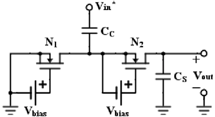
A conventional rectifying circuit is shown in Figure 2.2, where NMOS transistors (N1
and N2) are connected in series, the RF input terminal is connected in an intermediate node
through a coupling capacitor (CC) and the output terminal is connected to a smoothing capacitor
(CS). This structure can be composed of only NMOS or PMOS devices or of both.
During the negative half cycle of the RF signal, N1 is on saturation and N2 is on the
cutoff region, thus, no current flows towards the output. Capacitor CC is charged to the peak
value of Vin minus Vth. During the positive half cycle, N1 is on the cutoff region and N2 is on
Chapter 2 – RF energy harvesting
12
RF source and by capacitor CC, thus, it is charged to twice the peak value of Vin minus twice
Vth. Therefore, the output voltage Vout is given by:
𝑉𝑜𝑢𝑡 = 2(𝑉𝑖𝑛− 𝑉𝑡ℎ) (2.6)
Figure 2.2 – Conventional CMOS rectifier using NMOS transistors.
The majority of power losses occurs due to the turn-on Vth of the MOS transistor. The
effective turn-on Vth of a diode-connected MOSFET is almost equal to the Vth of the MOS
transistor, which is typically less than that of a p-n junction diode, nonetheless, greater than the Vth of a Schottky diode. Therefore, a rectifier that uses this simple diode-connected
configuration cannot achieve a large PCE [38].
Since Vth is the main parameter responsible for degrading the performance of the
rectifier, the PCE can be improved by reducing Vth [38]. Various Vth cancellation techniques
have been reported and will be described in the following subsections.
2.2.1 External-Vth-cancelation technique
Figure 2.3 presents a schematic of a rectifier using external-Vth-cancellation technique
(EVC), where the gates are biased by an external voltage (Vbias) and the threshold voltage of
this configuration changes to Vth – Vbias [41]. Maximum output voltage is obtained when the
threshold voltage is negligible, i. e., when Vbias equals Vth. In this condition, the output voltage
is given by:
𝑉𝑜𝑢𝑡 = 2𝑉𝑖𝑛 (2.7)
However, this approach is not feasible for completely passive rectifiers since another DC supply is required.
Chapter 2 – RF energy harvesting
Figure 2.3 – NMOS rectifier using EVC technique to compensate the Vth.
2.2.2 Internal-Vth-cancelation technique
To overcome the use of an external source to bias the gates of the MOS devices, another approach for providing a DC bias voltage is the use of a voltage divider at the output of the rectifier (Figure 2.4). This method is known as internal-Vth-cancellation (IVC) technique [42].
This configuration is comprised of two voltage dividers composed of diode-connected MOSFETs and resistors. The MOS devices of the voltage dividers are identical to the ones of the rectifier, in order to ensure a correct bias voltage is generated. Since no DC supply rails are required, this method can be used for passive rectifier devices. Nevertheless, drawing current for the voltage divider reduces the efficiency of the rectifier.
Chapter 2 – RF energy harvesting
14
2.2.3 Self-Vth-cancelation technique
Another alternative is the use of self-Vth-cancellation (SVC) technique, where the gates
of the NMOS and PMOS transistors are connected to the highest (output) and lowest potential (ground) terminals, respectively (Figure 2.5). Using this SVC structure, the effective Vth of the
MOS transistors is reduced, when the output voltage is higher than 0 V, due to the increase of VGS, and no DC supply nor the draw of current from the output of the rectifier are required [38].
In addition to reducing the loss due to the reduction of Vth, this configuration is able to operate
under lower input powers.
Figure 2.5 – SVC rectifier configuration.
The energy loss in this configuration is mainly dependent on the turn-on resistance of the MOS transistors, when Vth is not so small and the reverse leakage current is negligible.
When Vth is quite small, reverse leakage current will reduce the PCE. Therefore, achieving both
small forward bias resistance and small leakage current is not possible using this configuration [38].
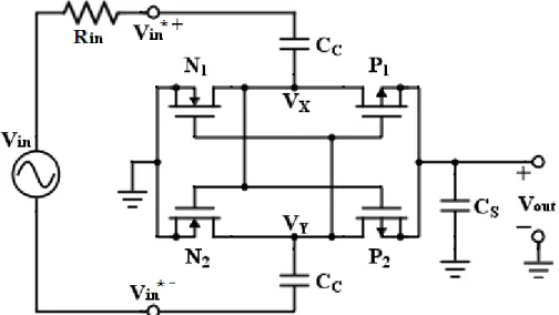
2.2.4 Differential rectifier
The differential circuit of Figure 2.6 allows to overcome the issues of the previous configuration. It uses a SVC technique, where the output of the rectifier biases its own MOS devices, thus, reducing the effective Vth [38]. It is composed of two pairs of MOS transistors,
the gates of which are connected to the drains of the opposite pair and to one end of the input terminal through capacitors CC. When the voltage at the gates of the MOS devices is positive,
the NMOS transistor is turned on. For instance, when the voltage at node VX is negative, N1 is
Chapter 2 – RF energy harvesting
forward bias resistance. On the other hand, when the voltage at gate terminals is negative, the PMOS transistor is turned on. For instance, when voltage VX becomes positive and N1 is turned
off, the voltage at its gate decreases and effectively reduces the reverse leakage current [38]. The gates of the transistors are statically biased by the common-mode voltage and actively biased by a differential-mode signal, thus, compensating the threshold voltage of the MOS devices [38]. This configuration overcomes the issues of the rectifier configurations described, hence, this was the rectifier implemented for RF-DC conversion.
This full-wave rectifying circuit is equivalent to the circuit of Figure 2.7.
Figure 2.7 – Circuit equivalent to the SVC differential rectifier topology presented in Figure 2.6.
Figure 2.6 – SVC differential rectifier topology. Transistors N1 and P1 comprise the MOS pair 1 and N2 and P2
Chapter 2 – RF energy harvesting
16
2.3 Rectifying system on PCB
To determine the conditions to which the CMOS circuit will be exposed, another circuit was implemented using off-the-shelf components, in a printed circuit board (PCB). Several types of RF-DC rectifiers using off-the-shelf discreet components have been reported in the literature and will be discussed in following subsections.
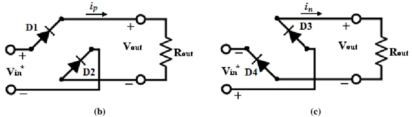
2.3.1 Bridge topology
The bridge RF rectifier provides a full-wave rectification, however, is a seldom used configuration for a RF rectifier [43]. As seen in Figure 2.8 (a), the bridge rectifier is composed of a diode bridge and an output load. Since the DC currents generated from the two branches cancel each other at the input port, no reactive component is required at the output port the bridge RF rectifier [44].
The diodes are turned on and allow current to pass, when the junction voltage (Vj) is
higher than or is equal to Vth; and are turned off and do not allow current to pass, when Vj is
lower than Vth. When Vin is positive (Figure 2.8 (b)) and is superior to or equals 2Vth, diodes
D1 and D2 are turned on, diodes D3 and D4 are turned off and current ip flows. In contrast,
when Vin is negative (Figure 2.8 (c)) and is inferior to or equals –2Vth, diodes D1 and D2 are
turned off, diodes D3 and D4 are turned on and current in flows. As observed in Figure 2.8 (b)
and Figure 2.8 (c), both ip and in currents flow in the same direction for the output load. The
output voltage is given by:
𝑉𝑜𝑢𝑡 = 𝑉𝑖𝑛 − 2𝑉𝑡ℎ (2.8)
Chapter 2 – RF energy harvesting
(b) (c)
Figure 2.8 – (a) Bridge RF rectifier topology. (b) Current pathway when diodes D1 and D2 are turned on, and
diodes D3 and D4 are turned off. (c) Current pathway when diodes D1 and D2 are turned off, and diodes D3 and D4 are turned on.
The operation of bridge RF rectifier can be further enhanced, by adding a shunt capacitor to the output load. In addition to enhancing the PCE by increasing the DC output-matching, this smoothing capacitor also allows to reduce the output ripple [44].
2.3.2 Double voltage topology
The Greinacher rectifier or voltage doubler is composed of two diodes and two capacitors, as shown in Figure 2.9 (a). This circuit is a half-wave rectifier, since only the positive half cycles of the input signal are rectified [45].
When Vin* is negative and is lower than or equals –Vth, diode D2 is turned off and does
not allow current to pass through capacitor C2 and the output load Rout, and diode D1 is turned
on, thus, charging capacitor C1 to the peak value of Vin* minus Vth (Figure 2.9 (b)). When Vin*
is positive and is higher than or equals Vth, diode D1 is turned off and diode D2 is turned on,
charging capacitor C2 by both the source and capacitor C1, as they have the same polarities. Therefore, C2 is charged to twice the amplitude of Vin* minus twice Vth (Figure 2.9 (c)) [45].
A full-wave rectifier is obtainable from the Greinacher circuit by mirroring the latter. This circuit acts as a voltage quadrupler (Figure 2.10). By cascading this circuit as, it is possible to achieve a higher output voltage [45].
Chapter 2 – RF energy harvesting
18 (a)
(b) (c)
Figure 2.9 – (a) Greinacher double-voltage rectifying circuit, and its behavior during (b) the negative half cycle
and (c) the positive half cycle.
Figure 2.10 – Full-wave voltage quadrupler.
2.3.3 Double current topology
Applying the duality theorem to the circuit of Figure 2.9 (a) results in the double current rectifying circuit of Figure 2.11 [44], [46]. The latter circuit is the opposite of the first one as the output voltage is half the input voltage and the output DC current is twice the input current. Therefore, the circuit of Figure 2.11 is a current doubler and a voltage divider. The procedure of applying duality to voltage multiplier circuits can be extended to higher order multipliers to produce current multipliers of the same order [46].
Chapter 2 – RF energy harvesting
During the negative half cycle, diode D1 is turned off and the inductor L1 is charged, storing the input current iin. During the positive half cycle, diode D1 is turned on and diode D2
is turned off, charging inductor L2 with the currents of both L1 and the source, delivering a current of 2iin to the output load.
Figure 2.11 – Double-current rectifying circuit.
2.3.4 Single-series topology
Figure 2.12 presents a simple half-wave RF rectifier, composed of a single diode, an inductor and a capacitor. During the negative half cycle, the diode is turned off and the inductor is charged. When the diode starts conducting, during the positive half cycle, when Vin is higher
than or equals Vth, current flows from the source and the inductor towards the capacitor and the
output load. The inductor, in addition to making a DC ground path from the diode to the load, chokes current iL against RF current; and the capacitor is responsible for the RF ground path
from the source to the diode and for reducing the output ripple [44], [47].
Figure 2.12 – Single-series diode topology.
Taking the described configurations and the desired application into consideration, as well as the components available, the single-series diode rectifier was implemented on a PCB.
Chapter 2 – RF energy harvesting
20
The current doubler is a voltage divider and, since the highest possible voltage is desired to be delivered to the load, for the intended application, this is the least appropriate topology. The available Schottky diodes present a 0.7 V forward voltage drop [48] and, therefore, it consists of a 1.4 V voltage drop for the multi-diode topologies presented. Thus, the output voltage obtained using the bridge configuration or the voltage doubler is greatly degraded due to the voltage drop in each diode and high input powers are necessary to overcome this issue. The single-series diode topology is, thus, able to operate under lower input powers.
3
C
HAPTER
3
–
PCB
RF-DC
CONVERTER DESIGN
As stated in Chapter 2, the single-series diode topology was chosen as the RF-DC rectifying circuit, using discreet off-the-shelf components. The aim of implementing this circuit is to prepare the appropriate setup and promptly understand the conditions at which the CMOS circuit will be exposed, when performing tests.
A board was designed to implement and test the rectifier, and its behavior was simulated, using a finite element analysis software (the simulation results are described and discussed in Chapter 5).
Even though the rectified DC output voltage might be quite low, it may be used to charge the battery of low-power devices. Therefore, a commercial low-power battery charger, powered by the rectifier’s output, was used to power a 470 mF supercapacitor [49]. Consequently, another board containing the rectifier and the battery charging circuit was designed.
The following sections describe the implementation of the rectifying circuit, the design of the boards and the operation of the battery charger.
3.1 Board design
The rectifying circuit is composed of a coplanar waveguide (CPW) transmission line (Figure 3.1), which was printed on a 60 mil (1.524 mm) thickness Arlon MED AD250A substrate (εr = 2.5) [50].
Figure 3.1 – Cross-section of a coplanar waveguide transmission line.
The board was designed and its dimensions were optimized using software HFSS. This optimization was done by creating a model of the AD250 Arlon substrate and by simulating the
Chapter 3 – PCB RF-DC converter design
22
S11 and S21 parameters of the transmission line and adjusting its dimensions based on the value
of S11 for a range of frequencies, considering the characteristic impedance to be the standard
50 Ω impedance. The optimized dimensions were the width of the ground reference and the conductor lines and the separation between them.
If the transmission line has an impedance different from the 50 Ω standard impedance of the used equipment, there is an impedance mismatch, which results in signal degradation and part of it is reflected, as maximum power delivery is only achieved when the impedance of all components is the same [28].
Considering the transmission line a two-port network, the S11 parameter is the input port
voltage reflection coefficient, when port 2 is terminated in a matched load [51], [52], and gives a measurement of impedance matching: if its value is below –10 dB (common bandwidth limit for the S11 so that the impedance matching state is acceptable), then the impedances are
considered to be matched [53]. The S21 parameter is the transmission coefficient from port 1 to
port 2, when port 1 is terminated in a matched load. The higher the value of S21, the more signal
is transferred from port 1 to 2 [51], [52].
The simulations were performed, firstly, ignoring the discontinuity on the conductor strip due to the series diode and, then, taking this discontinuity into account. When considering the discontinuity, the effect of the diode in the transmission line was regarded as short-circuit, the length of which is approximately the distance between the pads of the diode (0.3 mm) and width corresponds to the width of the pads (0.2 mm).
Several geometries for the discontinuity caused by the series diode were evaluated (different linear and partial linear tappers were tested for the compensation of the step discontinuity) and the one which produced the lowest value of S11 was selected. The step
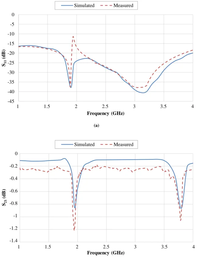
discontinuity caused by the diode was not compensated (Figure 3.2 (a)), as this geometry displayed the lowest S11 and the highest S21 for the desired frequency range (1 GHz to 4 GHz).
Figure 3.3 displays the S-parameters (simulated and measured) of the transmission lines printed on the Arlon-MED substrate (short-circuited on the area intended for the diode, as described above and observed in Figure 3.2 (c)) for frequencies between 1 GHz and 4 GHz. For the entire frequency range, the curves of the simulated and measured S11 parameter is below
–10 dB, as observed in Figure 3.3 (a), thus, the impedance of the transmission line is well matched. Moreover, in Figure 3.3 (b), both curves of the S21 parameter are close to 0 dB,
indicating most of the signal applied to the transmission line is transferred to its output [51], [52].
Chapter 3 – PCB RF-DC converter design
(a)
(b)
(c)
Figure 3.2 – (a) Transmission line, (b) gap dimensions and (c) short-circuit dimensions used for design
simulations, printed on a 5x5cm board made of Arlon-Med 60 mil AD250A substrate (not drawn to scale).
Even though the measured and simulated S-parameters do not completely overlap for the frequencies considered, the curves have approximately the same profile and the maximums and minimums occur at the same frequencies. This may be due to the losses from the transition from the coaxial cable to the CPW via the SMA connector, since this component was not accounted in the simulations. Additionally, in the simulation, the material was considered to be a perfect conductor, because the used Arlon substrate is low-lossy. Although the losses are small, they still occur since, in reality, a perfect conductor does not exist, which explains the measured S21 curve being below the simulated one (Figure 3.3 (b)).
Despite the differences observed between the simulated and the measured S-parameters, it can be concluded the impedance of the designed transmission line is well matched for its use with 50 Ω standard impedance equipment.
Chapter 3 – PCB RF-DC converter design
24 (a)
(b)
Figure 3.3 – Simulated and measured (a) S11 and (b) S21 parameters (in dB) of the transmission line printed on
the 60 mil AD250A substrate, for frequencies between 1 GHz and 4 GHz.
-45 -40 -35 -30 -25 -20 -15 -10 -5 0 S11 (d B ) Frequency (GHz) Simulated Measured S21 (d B ) Frequency (GHz) Simulated Measured 1 1.5 2 2.5 3 3.5 4 0 -0.2 -0.4 -0.6 -0.8 -1 -1.2 -1.4 1 1.5 2 2.5 3 3.5 4
Chapter 3 – PCB RF-DC converter design
3.2 Rectifying circuit operation
As seen in Figure 3.4, the rectifying circuit is comprised of a 1 μH inductor, a Schottky rectifying diode (MACOM MADS-001317-1500AG [48]) and a 1.2 pF capacitor. As mentioned in Chapter 2, Schottky diodes have some advantages in RF applications comparing with conventional diodes [39].
As reviewed in the previous chapter, the inductor behaves as a RF choke and allows lower frequencies and DC current to pass and is responsible for the blockage of the high frequencies of the RF signals; the Schottky diode placed in series rectifies the input wave and the capacitor shorts the RF energy and permits the DC output signal to pass [44].
Figure 3.4 – Schematic of the rectifying circuit composed of a 1 µH inductor, a Schottky diode and a
1.2 pF capacitor.
The rectifier’s output voltage is determined by adding a resistive load and measuring the voltage drop across this component. Since the magnitude of the load has an impact in the power received, the load was replaced by a variable resistor in order to measure the preferable value. Using Agilent Technologies vector network analyzer (VNA) (E8358A PNA – 300 kHz to 9 GHz) as a RF signal generator, applying the signal to the input of the rectifier, for the frequency range of 1 GHz to 4 GHz, and measuring the voltage across the load enabled to compute the output power and determine the preferable value. Firstly, the current flowing through the load was calculated, using Ohm’s law. Knowing both the voltage and current on the load the output DC power (in dBm) could be obtained as follows:
𝑃 = 𝑉 × 𝐼 (3.1)
𝑃𝑑𝐵𝑚 = 10 × log10( 𝑃
1 𝑚𝑊) (3.2)
where 𝑉 is the voltage across the load, 𝐼 is the current flowing through it, 𝑃 is the power, in SI units, and 𝑃𝑑𝐵𝑚 is the power in dBm. Figure 3.5 presents the output powers obtained in the measurements performed for three different output loads.
Chapter 3 – PCB RF-DC converter design
26
The preferable load value was found to be 1 kΩ and this load was added to circuit and included in further tests and simulations. Figure 3.6 presents the rectifying circuit and the 1 kΩ load implemented on the board.
Figure 3.5 – Converted output DC power (in dBm) obtained with 100 Ω, 1 kΩ and 10 kΩ output loads, for
frequencies between 1 GHz and 4 GHz and 0 dBm input power.
Figure 3.6 – Rectifying circuit implemented on the board described in the previous section.
-70 -60 -50 -40 -30 -20 -10 0 C on ve rt ed P ow er ( d B m ) Frequency (GHz) 100 Ω 1 kΩ 10 kΩ
RF
DC
input
output
1 1.5 2 2.5 3 3.5 4Chapter 3 – PCB RF-DC converter design
Models of the diode and the transmission line were created, based on the specifications referred on the datasheet, to simulate the S11 parameter of the rectifier implemented on board
described on the previous section. The distance between the components on the PCB and the dimensions of the transmission line were also taken into consideration, in the simulation (Figure 3.7).
Figure 3.7 – System used to simulate the S11 parameter of the implemented PCB, evidencing the distances
between components and the dimensions of the CPW (not drawn to scale).
The behavior of the rectifier was assessed by computing its S11 parameter for
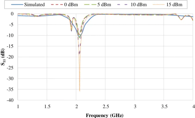
frequencies between 1 GHz and 4 GHz. Observing Figure 3.8, which presents the simulated (for 0 dBm input power) and measured (for different input powers) S11 curves of the rectifier,
it is concluded that the results from the simulation do not overlap the experimental results for most frequencies. The electrical specifications of diode referred on the datasheet used to create the model of the diode were limited, which may have influenced the results, however, the simulated and experimental curves have approximately the same profile and the minimum occurs at the same frequency. Despite the observed differences between the simulation and the experimental measurements, the behavior of the circuit is similar in both cases.
At approximately 2 GHz, the S11 parameter is below –10 dB for the simulation and the
experimental measurements, thus, the impedance of the circuit is less mismatched thus a better performance is expected at this frequency. Since this system has a very narrow bandwidth, it is appropriate only for rectifying energy harvested from a dedicated source.
The efficiency of the RF-DC conversion using the proposed circuit, as well as its suitability for wireless energy transfer, for a range of frequencies, and the tests performed to assess these parameters are described in Chapter 5.
Chapter 3 – PCB RF-DC converter design
28
Figure 3.8 – Measured (for 0 dBm, 5 dBm, 10 dBm and 15 dBm input powers) and simulated (0 dBm input
power) S11 parameter (in dB) of the implemented rectifier with a 1 kΩ load, for frequencies ranging from 1 GHz
to 4 GHz.
3.3 Final RF-DC converting system
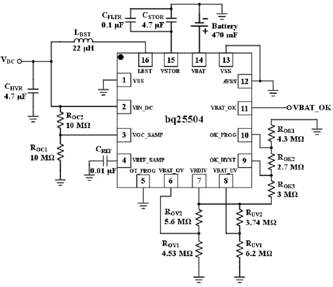
Once proven the circuit does indeed rectify RF signals to DC ones, its output was used to power a commercial low-power battery charging circuit (Texas Instruments BQ25504), which is used to charge a battery. Figure 3.9 shows the schematic of the battery charging system, composed of the rectifier and the battery charging circuit.
Figure 3.9 – Schematic of the battery charging system.
Another board, which contains the RF-DC rectifier and the charging circuit, was designed (Figure 3.10). This PCB was implemented using the same Arlon MED substrate as the previous board.
-40 -35 -30 -25 -20 -15 -10 -5 0 S11 (d B ) Frequency (GHz) Simulated 0 dBm 5 dBm 10 dBm 15 dBm 1 1.5 2 2.5 3 3.5 4
Chapter 3 – PCB RF-DC converter design
Figure 3.10 – Board designed for the rectifier and the battery charging circuit.
The following sections describe the implantation of the rectifier and the charging circuit that comprise this system.
3.3.1 Rectifying circuit
Since the previously implemented rectifier’s performance was satisfactory (described in Chapter 5), the same circuit was employed in this approach. The dimensions of the CPW (width and spacing between conductor and ground planes) and the diode’s gap discontinuity were replicated. The distance between the components was also the same as depicted in Figure 3.7.
3.3.2 Battery charging circuit
Since rectifier’s output and the voltages involved in the charger are DC, it was not necessary to design the board’s vias with a 50 Ω impedance. Therefore, the fabrication limit dimensions regarding via width were used (0.254 mm), as seen in Figure 3.10.
Texas Instruments’ bq25504 is an ultra-low power with high efficiency DC/DC boost charger with programmable dynamic Maximum Power Point Tracking (MPPT) algorithm. MPPT is a technique that allows varying the electrical operating point, by determining the adequate load, so that the system delivers the maximum available power [54]. Figure 3.11 displays the battery charging circuit used in this work and its operation is described as follows.
Chapter 3 – PCB RF-DC converter design
30 Figure 3.11 – Low-power battery charging circuit.
Firstly, the charger rapidly charges up the capacitor CSTOR. If a storage element is connected, it attempts to charge up CSTOR using the storage element for approximately 45 ms, and afterwards powers its internal circuits from the voltage on pin 15 (VSTOR). As soon as the pin VSTOR reaches the under voltage threshold (VBAT_UV) established by the user, the charger starts to charge the storage element, if a sufficient amount of power is available at pin 2 (VIN_DC). If pin VSTOR does not reach the voltage VBAT_UV within 45 ms, the cold-start subsystem turns on. If the voltage at pin VIN_DC is greater than at pins VSTOR or VBAT (pin 14), current may flow until the voltage on pin VIN_DC decreases or the voltage on pins VSTOR and VBAT increases [55].
When the voltage on pin VIN_DC is higher the minimum input voltage with sufficient power, the cold-start subsystem, which consists of an unregulated boost converter, turns on. When the voltage on CSTOR reaches 1.8 V, the main boost regulator is started. VSTOR voltage

![Figure 3.12 – Different voltages and operation modes of the device [55].](https://thumb-eu.123doks.com/thumbv2/123dok_br/17694797.827878/50.892.153.748.115.534/figure-different-voltages-operation-modes-device.webp)
