Abstract—A closed-loop reconfigurable 4×/3×/2×/1×
switched-capacitor (SC) boost DC-AC inverter is proposed by combining a sinusoidal pulse-width-modulation (SPWM) controller for low-power step-up inversion and regulation. In this SC inverter, there are three pumping capacitors and 13 bidirectional switches between supply source and output terminal not only to boost the maximum gain up to 4, but also to invert the output voltage for DC-AC conversion. Here, this SC inverter is a reconfigurable structure to select the boosting gain of 4×, 3×, 2×, or 1× according to the desired output voltage
so as to improve the power efficiency, especially for the lower desired voltage. Further, the SPWM control is employed in order to enhance output regulation capability for the various outputs (output peak value or output frequency). Finally, the closed-loop SC boost inverter is simulated by OrCAD, and all results are illustrated to show the efficacy of the proposed scheme.
Index Terms—reconfigurable switched-capacitor, boost DC- AC inverter, sinusoidal pulse-width-modulation, bidirectional.
I. INTRODUCTION
ITH the popularity of portable electronic equipments, e.g. digital camera, e-book, mobile phone, notebook, and PDA …etc., the power modules of these products always asks for some good characteristics: small volume, light weight, higher efficiency, and better regulation capability. Generally, the traditional power converters have a large volume and a heavy weight because of magnetic elements. So, more manufactures and researchers pay much attention to this topic, and ultimately, requiring DC-DC or DC-AC converters realized on a compact chip by mixed-mode VLSI technology.
The SC-based power converter has received more and more attention because it contains semiconductor switches and capacitors only. Thus, this kind of SC converters is one of the good solutions for low-power DC-DC/DC-AC conversion. Unlike the traditional converter, the SC converter needs no magnetic element, so it always has a small volume and a light weight. The SC converter is usually designed for an output higher than supply voltage or a reverse-polarity voltage. This function fits many applications,
Manuscript received December 2, 2011. This work is supported in part by the National Science Council of Taiwan, R.O.C., under Grant NSC 100-2221-E-324-005.
Yuen-Haw Chang and Jia-Jie Liao are with the Department and Graduate Institute of Computer Science and Information Engineering, Chaoyang University of Technology, Taichung, Taiwan, R.O.C. Post code: 413. (e-mail:
[email protected], [email protected]).
e.g. drivers of electromagnetic luminescent (EL) lamp, white light emitting diode (WLED), op-amp, and LCD drivers. In fact, the SC idea has existed over half a century. In 1990, the first SC step-down converters were proposed by Japan researchers [1], and their idea is to switch MOSFETS cyclically according to 4 periods of capacitors charging/ discharging for step-down conversion. In 1993, Cheong et al. suggested a modified SC converter with two symmetrical SC cells working in the two periods [2]. Then, combining with pulse-width-modulation (PWM) technique, they proposed a new step-up DC-DC converter by using duty-cycle control [3]. In 1994, Ngo et al. first proposed a current control of SC converters by using a saturated transistor as a controllable current source [4]. In 1996, Chung and Ioinovici suggested a current-mode SC for improving current waveforms [5]. In 1998, Mak and Ioinovici suggested an SC inverter with high power density [6]. Following this idea, Chang proposed an integrated SC step-up/down DC-DC/DC-AC converter [7-10].
In this paper, a closed-loop reconfigurable 4×/3×/2×/1× SC
boost DC-AC inverter is proposed not only for enhancing full-wave output regulation via SPWM technique, but also for improving the efficiency via reconfigurable topology.
II. SCHEME OF RECONFIGURATION SC BOOST DC-AC INVERTER
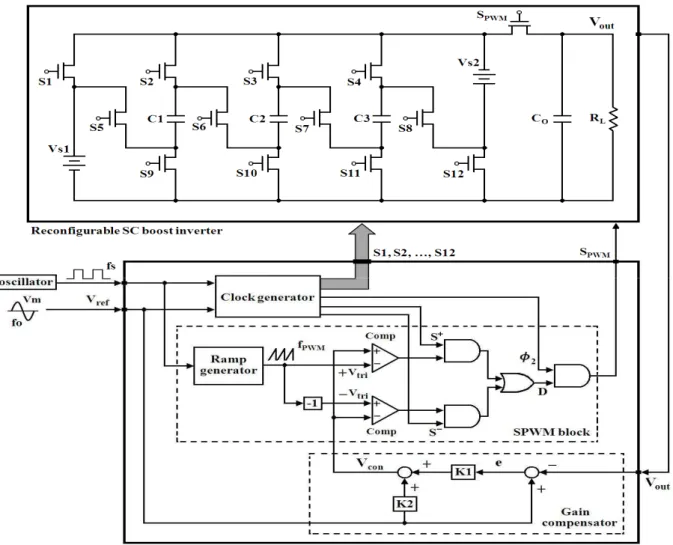
Fig. 1 shows the close-loop reconfigurable 4×/3×/2×/1× SC
boost DC-AC inverter, and it contains a power part and a control part. The discussions are as follow.
A. Power Part
The SC boost inverter as in the upper of Fig.1 is composed of 13 bidirectional switches devices (S1-S12 and SPWM), 3 pumping capacitor (C1-C3) and output capacitor CO between supply sources Vs1, Vs2 (Vs1=Vs2=Vs), and output Vout, where each capacitor has the same value C (C1=C2=C3=C). The main function of this power part is to boost Vout up to 4×, 3×, 2×, and 1× of Vs1 in positive half-wave, or to 4×, 3×,
2×, and 1× of Vs2 in negative half-wave. Thus, this part can
provide the output range of +4Vs ~ -4Vs for realizing DC-AC conversion. Now, these operations are discussed below.
1)Positive Half-Wave (PHW): a) Phase I:
S1, S2, S3, S4, S9, S10, S11 turn on, and S5, S6,
Reconfigurable 4
×
/3
×
/2
×
/1
×
Switched-Capacitor
Boost DC-AC Inverter
Yuen-Haw Chang and Jia-Jie LiaoS7, S8, S12, SPWM turn off. The relevant topology is shown in Fig. 2(a). C1, C2, C3 are charged by Vs1 in parallel.
b) Phase II:
In order to obtain the various voltage gains (4×, 3×,
2×, 1×), the different phase II operations (switches
and topologies) are explained below. (i) 4×:
S4, S5, S6, S7, SPWM turn on, and S1, S2, S3, S8, S9, S10, S11, S12 turn off. The current flow is passing via Vs1, C1, C2 and C3 in series connection through S4, S5, S6, S7, SPWM to output terminal as shown symbol “———” in Fig. 2(b). So, the 4× function can be obtained
with the help of Vs1, C1, C2 and C3 in series. (ii) 3×:
S3, S5, S6, S7, SPWM turn on, and S1, S2, S4, S8, S9, S10, S11, S12 turn off. The current flow is passing via Vs1, C1 and C2 in series connection through S3, S5, S6, SPWM to output terminal as shown symbol “-x-x-” in
Fig. 2(b). So, the 3× function can be obtained
with the help of Vs1, C1 and C2 in series. (iii) 2×:
S2, S5, S6, S7, SPWM turn on, and S1, S3, S4, S8, S9, S10, S11, S12 turn off. The current flow is passing via Vs1 and C1 in series connection
through S2, S5, SPWM to output terminal as shown symbol “-‧-‧-” in Fig. 2(b). So, the
2× function can be obtained with the help of Vs1
and C1 in series. (iv) 1×:
S1, S5, S6, S7, SPWM turn on, and S2, S3, S4, S8, S9, S10, S11, S12 turn off. The current flow is passing from Vs1 through S1, SPWM to output terminal as shown symbol “----- ” in Fig.
2(b).
2)Negative Half-Wave (NHW): a) Phase I:
S2, S3, S4, S9, S10, S11, S12 turn on, and S1, S5, S6, S7, S8, SPWM turn off. The relevant topology is shown in Fig. 2(c), C1, C2, C3 are charged by Vs2 in parallel.
b) Phase II:
In order to obtain the various voltage gains (4×,
3×, 2×, 1×), the different phase II operations
(switches and topologies) are explained below. (i) 4×:
S6, S7, S8, S9, SPWM turn on, and S1, S2, S3, S4, S5, S10, S11, S12 turn off. The current flow is passing via Vs2, C1, C2 and C3 in series connection through S6, S7, S8, S9, SPWM to output terminal as shown symbol “———” in Fig.1. Configuration of SC boost DC-AC inverter.
Fig. 2(d). So, the 4× function can be obtained
with the help of Vs2, C1, C2 and C3 in series. (ii) 3×:
S6, S7, S8, S10, SPWM turn on, and S1, S2, S3, S4, S5, S9, S11, S12 turn off. The current flow is passing via Vs2, C2 and C3 in series connection through S7, S8, S10, SPWM to output terminal as shown symbol “-x-x-” in Fig. 2(d). So, the
3× function can be obtained with the help of Vs2,
C2 and C3 in series. (iii) 2×:
S6, S7, S8, S11, SPWM turn on, and S1, S2, S3, S4, S5, S9, S10, S12 turn off. The current flow is passing via Vs2 and C3 in series connection through S8, S11, SPWM to output terminal as shown symbol “-‧-‧-” in Fig. 2(d). So, the
2× function can be obtained with the help of Vs2
and C3 in series. (iv) 1×:
S6, S7, S8, S12, SPWM turn on, and S1, S2, S3, S4, S5, S9, S10, S11 turn off. The current flow is passing from Vs2 through S12, SPWM to output terminal as shown symbol “----- ” in Fig.
2(d).
As above, Fig. 3 shows the theoretical waveforms of these switches S1-S12. In this paper, we design a clock generator (a)
(b)
(c)
(d)
Fig. 2. (a) Phase I topology in PHW (b) Phase II topology in PHW (c) Phase I topology in NHW (d) Phase II topology in NHW. (4× :————,
3× : -x-x-, 2× : -‧-‧-, 1× : ----)
in the SPWM controller by using digital logic gates in order to generate these driver signals of S1-S12 just like the waveforms in Fig. 3.
B. Controller Part
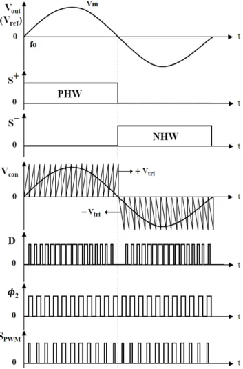
In the reconfigurable SC boost DC-AC inverter, the SPWM-based controller is used as shown in lower of Fig. 1. The controller is composed of an SPWM block, a clock generator, and a simple gain compensator. Form signal flow, Vout is sent into this compensator, and then the Vout is compared with Vref to obtain the tracking error e, as well as the control signal Vconvia gains K1 and K2, where K1 and K2 are the proportional gains to compensate the tracking error between Vout and Vref. Via the SPWM block, the waveforms of the basic SPWM duty-cycle signal D can be generated as in Fig. 4 by comparing Vcon with +Vtri (PHW) / -Vtri (NHW), and the comparing rules are listed as:
1)Positive Half-Wave (PHW): When Vcon>+Vtri, D=1.
When Vcon<+Vtri, D=0
2)Negative Half-Wave (NHW): When Vcon>-Vtri, D=0.
When Vcon<-Vtri, D=1.
With digital logic gates, the clock generator can be easily designed to obtain a set of non-overlapping complementary signalsψ1 andψ2. Based onψ1 andψ2, the control signals S1-S12 can be operated just like the waveforms in Fig. 3. The detailed Boolean relationships as follows: (“‧”: logic AND,
“+”: logic OR). S2=S3=S10=S11=ψ1, S6=S7=ψ2,
S1= (ψ1‧S+), S5= (ψ2‧S+), S12= (ψ1‧S-), S8= (ψ2‧S-), S4= (ψ1+S+), S9= (ψ1+S-).
In addition, to make sure the SPWM operation running in phase II, we take a logic AND between D andψ2 to obtain a practical SPWM duty-cycle signal SPWM as in Fig. 4 (SPWM = (ψ2‧D)). Based on this SPWM, the closed-loop output regulation capability can be enhanced for the various desired outputs.
III. EXAMPLE OF RECONFIGURATION SC BOOST DC-AC INVERTER
In this section, a closed-loop reconfigurable 4×/3×/2×/1×
SC boost DC-AC inverter with SPWM control is simulated by OrCAD, and then the results are illustrated to verify the efficacy of the proposed inverter scheme. All the parameters
are listed in Table I. There are 4 cases (4×/3×/2×/1×) to be
discussed as follows. 1)Case1: 4×
a) Frequency=1k:
Let the DC-AC booster supply source Vs1 and Vs2 be 5V, load RL be 1kΩ, and the peak value and output frequency of Vref are Vm=20V, fo=1kHz. And then, as shown in Fig. 5(a), Vout has the peak value of 19.235V, and the practical output frequency is about 1kHz. The efficiency is 72.54%, and THD is 4.45%. b) Frequency=0.8k:
Let the DC-AC booster source Vs1 and Vs2 be 5V, load RL be 1kΩ, and the peak value and output frequency of Vref are Vm=20V, fo=0.8kHz. And then, as shown in Fig. 5(b), Vout has the peak value of 19.242V, and the practical output frequency is about 0.8kHz. The efficiency is 72.25%, and THD is 4.09%.
2)Case2: 3×
a) Frequency=1k:
Let the DC-AC booster source Vs1 and Vs2 be 5V, load RL be 1kΩ, and the peak value and output frequency of Vref are Vm=15V, fo=1kHz. And then, as shown in Fig. 5(c), Vout has the peak value of 14.623V, and the practical output frequency is about 1kHz. The efficiency is 77.71%, and THD is 4.65%. b) Frequency=0.8k:
Fig. 5(a). 4× mode: Vout (Vref : Vm=20V, fo=1kHZ).
Fig. 5(b). 4× mode: Vout (Vref : Vm=20V, fo=0.8kHZ).
Fig. 5(c). 3× mode: Vout (Vref : Vm=15V, fo=1kHZ).
Fig. 5(d). 3× mode: Vout (Vref : Vm=15V, fo=0.8kHZ).
Fig. 5(e). 2× mode: Vout (Vref : Vm=10V, fo=1kHZ).
Fig. 5(f). 2× mode: Vout (Vref : Vm=10V, fo=0.8kHZ)
Fig. 5(g). 1× mode: Vout (Vref : Vm=5V, fo=1kHZ)
Fig. 5(h). 1× mode: Vout (Vref : Vm=5V, fo=0.8kHZ).
Let the DC-AC booster source Vs1 and Vs2 be 5V, load RL be 1kΩ, and the peak value and output frequency of Vref are Vm=15V, fo=0.8kHz. And then, as shown in Fig. 5(d), Vout has the peak value of 14.623V, and the practical output frequency is about 0.8kHz. The efficiency is 83.65%, and THD is 4.22%.
3)Case3: 2×
a) Frequency=1k:
Let the DC-AC booster source Vs1 and Vs2 be 5V, TABLEI
COMPONENTS OF RECONFIGURABLE SCBOOST INVERTER Supply source 5V
Pumping capacitor (C1~C3) 0.3uF Output capacitor (Co) 0.085uF Equivalent series resistor of
load RL be 1kΩ, and the peak value and output frequency of Vref are Vm=10V, fo=1kHz. And then, as shown in Fig. 5(e), Vout has the peak value of 9.8V, and the practical output frequency is about 1kHz. The efficiency is 82.56%, and THD is 7.98%.
b) Frequency=0.8k:
Let the DC-AC booster source Vs1 and Vs2 be 5V, load RL be 1kΩ, and the peak value and output frequency of Vref are Vm=10V, fo=0.8kHz. And then, as shown in Fig. 5(h), Vout has the peak value of 9.8V, and the practical output frequency is about 0.8kHz. The efficiency is 86.63%, and THD is 7.09%. 4)Case4: 1×
a) Frequency=1k:
Let the DC-AC booster source Vs1 and Vs2 be 5V, load RL be 1kΩ, and the peak value and output frequency of Vref are Vm=5V, fo=1kHz. And then, as shown in Fig. 5(g), Vout has the peak value of 5.074V, and the practical output frequency is about 1kHz. The efficiency is 65.61%, and THD is 21.15%.
b) Frequency=0.8k:
Let the DC-AC booster source Vs1 and Vs2 be 5V, load RL be 1kΩ, and the peak value and output frequency of Vref are Vm=5V, fo=0.8kHz. And then, as shown in Fig. 5(h), Vout has the peak value of 5.06V, and the practical output frequency is about 0.8kHz. The efficiency is 74.4%, and THD is
24.95%.
According to the above results, it is obvious that Vout is following Vref for the different output peaks, output frequencies, and boosting gains. These results show that this SC inverter has a good steady-state performance.
IV. CONCLUSION
A closed-loop reconfigurable 4×/3×/2×/1× SC boost
DC-AC inverter is proposed by combining a SPWM controller for low-power step-up inversion and regulation. Finally, the closed-loop SC boost inverter is simulated by OrCAD, and all results are illustrated to show the efficacy of the proposed scheme. The advantages of the scheme are listed as follows.
1)This SC-based inverter needs no large magnetic element. Thus, the IC fabrication is promising.
2)As we always see, it results in the efficiency degradation when the lower output voltage is desired. Here, our SC inverter is a reconfigurable structure in capable to select the boosting gain of 4×, 3×, 2×, or 1× according to the
desired output voltage so as to improve the power efficiency, especially for the lower desired voltage. 3)The SPWM control is employed here to enhance output
regulation capability for the various outputs (output peak value or output frequency).
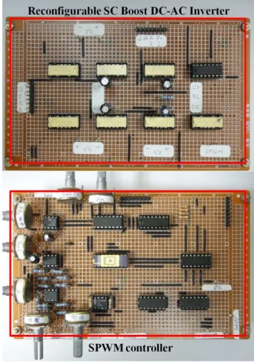
At present, we have implemented the hardware circuit of the reconfigurable SC boost inverter as the photo in Fig. 6. Next, some more experimental results will be measured for the verification of this scheme.
REFERENCES
[1] T. Umeno, K. Takahashi, I. Oota, F. Ueno, and T. Inoue, “New switched-capacitor DC-DC converter with low input current ripple and its hybridization,” in Proc. 33rd IEEE Midwest Symposium on Circuits and
Systems, Calgary,Canada, pp.1091-1094, 1990.
[2] S. V. Cheong, S. H. Chung, and A. Ioinovici, “Duty-cycle control boosts dc-dc converters,” IEEE Circuits and Devices Mag., vol.9, no.2, pp.36-37, 1993.
[3] O. C. Mak, Y. C. Wong, and A. Ioinovici, “Step-up DC power supply based on a switched-capacitor circuit,” IEEE Trans. on Industrial Electronics, vol.42, no.1, pp.90-97, 1995.
[4] K. D. T. Ngo and R. Webster, “Steady-state analysis and design of a switched-capacitor DC-DC converter,” IEEE Trans. Aerospace and
Electronic Systems, vol.30, pp.92-101, 1994.
[5] H. Chung and A. Ioinovici, “Switched-capacitor-based DC-to-DC converter with improved input current waveform,” in Proceedings IEEE
Int. Symp. Circuits and Systems, Atlanta, USA, pp.541-544, 1996.
[6] O. C. Mak and A. Ioinovici, “Switched-capacitor inverter with high power density and enhanced regulation capability,” IEEE
Trans.Cir-cuits Syst. I, Fundam. Theory Appl., vol. 45, pp. 336–347, 1998.
[7] Y.-H. Chang, “Design and analysis of power-CMOS-gate-based switched-capacitor DC-DC converter with step-down and step-up modes,” Int. J. Circuit Theory and Appl., vol.31, pp.483-511, 2003. [8] Y.-H. Chang, “Design and analysis of power-CMOS-gate-Based
Switched-Capacitor Boost DC-AC Inverter,” IEEE Trans. Circuits
Syst.-I: Fundamental Theory and Appl., vol.51, pp.1998-2016, 2004.
[9] Y.-H. Chang, “Design and analysis of multistage multiphase switched-capacitor boost DC-AC inverter,” IEEE Trans. Circuits and
Systems-I: Regular paper, vol. 58, no.1, pp. 205-218, Jan. 2011.
[10] Y.-H. Chang, “Variable-conversion-ratio multistage switched- capacitor-voltage-multiplier/divider DC-DC converter,” IEEE Trans.
Circuits and Systems-I: Regular paper, vol. 58, no.8, pp. 1944-1957,