598 Brazilian Journal of Physics, vol. 34, no. 2B, June, 2004
Magnetic Nanostructures for Lateral Spin-Transport Devices
Dirk Grundler, Thomas M. Hengstmann, and Haiko Rolff
Institut f¨ur Angewandte Physik und Zentrum f¨ur Mikrostrukturforschung, Universit¨at Hamburg Jungiusstrasse 11, D-20355 Hamburg, Germany
Received on 31 March, 2003
We review our investigations on nanostructured ferromagnets fabricated on semiconductor heterostructures. We show that ballistic electrons in the semiconductor are in particular sensitive to local stray fields. The reversal of the ferromagnets give rise to characteristic magnetoresistance traces in the ferromagnet/semiconductor hy-brid structures. We use these stray-field effects for detailed studies on the magnetic properties of rectangular micromagnets, nanodisks and nanorings. The nanostructures might be favorable candidates for ferromagnetic contacts in future spin-injection experiments in lateral feromagnet/semiconductor hybrid structures.
1
Introduction
Injection of spin-polarized currents into semiconductors is a challenging research field [1-4]. High spin injection effi-ciencies would render spintronics with semiconductors rel-evant for technological applications [5]. One of the most controversial issues in experiment [6-9] and theory [10] is the all-electrical spin injection and spin detection in a high-mobility two-dimensional electron system (2DES) using fer-romagnetic metals. We have recently developed a model to describeballistictransport in ferromagnet/semiconductor hybrid structures [11-13]. In this transport regime spin in-jection is possible by means of spin filtering at the ferro-magnet/semiconductor interface [12, 14]. Characteristic and pronounced spin-valve effects are predicted [13]. It has ear-lier been argued however that stray fields perpendicular to the plane of the 2DES could induce an additional magne-toresistance (MR) effect which might mimic a spin-valve effect [8]. This Lorentz-force induced MR effect is often called the local Hall effect. The latter is prominent in lateral ferromagnet/semiconductor hybrid structures rather than in the all-metal giant magnetoresistance (GMR) devices due to the smaller carrier density ns of the 2DES. An important prerequisite for the interpretation of transport phenomena in ferromagnet/semiconductor hybrid structures is therefore a good knowledge of the stray fields of the ferromagnetic contacts. We have investigated different nanostructured fer-romagnets with respect to the local Hall effect. Here, we review our recent experimental results.
2
Experimental setup
Mesoscopic 2DES which are sensitive to the local Hall ef-fect [15, 16] have been fabricated in a GaAs/Al0.3Ga0.7As
heterostructure using electron-beam lithography and pho-tolithography followed by a wet etching process. The het-erostructure has been grown by means of molecular beam epitaxy (MBE). Due to modulation doping it contains a
high-mobility 2DES 90 nm below the surface. The elec-tronic width of the etched Hall bar is in the order of 1µm. A typical device is shown in Fig. 1. Contacts are fabricated using evaporation and lift-off technique. The carrier density nsis2.7·10
11
cm−2and the mobilityµis350,000cm2/Vs at 4.2 K. Hence, the electron mean free path isle = 3µm. All experiments are performed at 4.2 K such that the elec-tron system is in the ballistic transport regime. The poly-crystalline permalloy (Ni80Fe20) micro- and nanomagnets
are integrated on the cap layer of the heterostructure us-ing electron beam lithography, evaporation and lift-off tech-nique (Fig. 1). The 20 nm thick permalloy film has been capped by a 9 nm gold layer. The ferromagnetic nanostruc-tures are electrically isolated from the 2DES. By this means, we are able to investigate in detail the stray field effects and to focus on Lorentz-force induced MR effects. For this, we have performed Hall and bend-resistance measurements on the mesoscopic 2DES. The bend resistance is a characteris-tic MR feature that originates from electrons travelling bal-listically through the 2DES [17].
The external magnetic fieldBis applied in the plane of the 2DES, i.e., the observed hysteretic features are solely due to stray fields of the ferromagnets which are perpendic-ular to the 2DES. The field B is swept in small steps of a few tenth of a mT. The currentIof amplitude 3µA applied to the 2DES is modulated at 37 Hz. The voltage is detected using lock-in technique.
3
Experimental results and
discus-sion
Dirk Grundleret al. 599
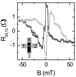
Figure 1. A two-micromagnet system fabricated from permalloy on top of the insulating cap layer of a Hall bar etched in a 2DES.
(II) a nanodisk and (III) a nanoring. The first has been pro-posed for spin-injection and spin-detection experiments in lateral ferromagnet/semiconductor hybrid structures in Ref. [18]. Nanodisks and nanorings have been proposed earlier to be interesting for GMR spin-valve devices [19].
Rectangular micromagnets
The Hall resistance measures the averaged magnetic flux in the 2DES [15, 16]. Recently we have shown that, in par-ticular, the bend resistance is sensitive to the local details of the field pattern penetrating the 2DES and that it is useful to enhance considerably the lateral resolution of a 2DES Hall bar [20]. This is demonstrated on sample (I) in Fig. 2. Here, the bend-resistance trace is shown which is measured on a 2DES cross junction containing a two-micromagnet system (compare Fig. 1) with a separationd= 200nm. The four contact leads are labelled with 1 to 4 (inset of Fig. 2). The current is injected between the leads 2 and 4 and the voltage is measured between the contacts 1 and 3. By this means, electrons are detected at contact 1 which transverse the cross junction ballistically [17] and which enter the voltage probe 1 without being deflected by the inhomogeneous stray field. The bend resistance R24,13 shows a hysteretic
’butterfly’-like shape which is interesting by itself. Here it is important that the stray field gives rise to a character-istic and pronounced MR effect for the ballistic electrons in the mesoscopic 2DES. In micromagnetic simulations we have found that the change of the domain pattern in the two-micromagnet system occurs very local within sub-micron domains. The experimental result is that ballistic electrons in the 2DES are very sensitive to these local stray fields [20], i.e., the Lorentz-force induced MR effect reflects in detail the magnetic behavior of the ferromagnets on the nanometer scale. In Fig. 2 the bend resistance is nonzero for almost all magnetic fields. Near zero magnetic field, i.e., in the remanent state, the bend resistance is in particular either positive or negative depending on the magnetic history. As a result, we find that a ballistic 2DES beneath a rectangular two-micromagnet system shows a very complex MR caused by the stray fields.
Figure 2. Bend resistance measured on a 2DES cross junction be-neath a two-micromagnet system. The current is injected through the leads 2 and 4, the voltage drop is measured between the leads 1 and 3. The configuration and the lead numbers are sketched in the inset. The zero-field resistance value has been subtracted from the data. Data were taken from Ref. [21].
Nanodisks
It has early been argued [19] that nanomagnets with a circular shape fabricated from permalloy might be a favor-able candidate for spin-valve devices. Only very recently the intriguing magnetic properties of nanodisks have been verified experimentally [22]. In the remanent state of a nan-odisk the microscopic magnetic moments should be in the plane of the disk and arranged in a clockwise or counter-clockwise manner. In the center, there should exist a vortex which would give rise to a small stray field perpendicular to the plane of the disk.
We have fabricated nanodisks on mesoscopic 2DES and have investigated the stray-field effects [23]. The MR ef-fect is found to be less complex if compared to rectangular micromagnets (Fig. 3). The important finding is that the lo-cal Hall effect follows very nicely the lo-calculated hysteretic magnetization loop.
A comparison between simulated magnetizationMand Hall measurementRH is shown in Fig. 3 [sample(II)]. We find a good qualitative agreement. Only at zero magnetic field, i.e., in the remanent state, we observe a small discrep-ancy between the local Hall effect and the magnetization curveM vs. B. In the experimental data, there is an off-set inRHbetween the up sweep and the down sweep of the magnetic fieldB. This seems to reflect the chirality of the remanent magnetic state of the nanodisk and the orientation of the vortex which is formed in the central region of the nanodisk.
Nanorings
600 Brazilian Journal of Physics, vol. 34, no. 2B, June, 2004
Figure 3. Comparison between the data of the Hall resistanceRH
of a 2DES beneath a permalloy nanodisk withd = 700nm and thicknesst= 20nm (open symbols) and a simulated magnetiza-tion curveM vs. B (filled symbols). Both data show large irre-versible jumps near zero field. Calculated domain configurations are depicted in a greyscale plot for the variation ofB from posi-tive to negaposi-tive values (A-E) and one configuration for the reverse sweep (F), the arrows indicate the direction of the magnetization vectors. Graph and data are taken from Ref. [23].
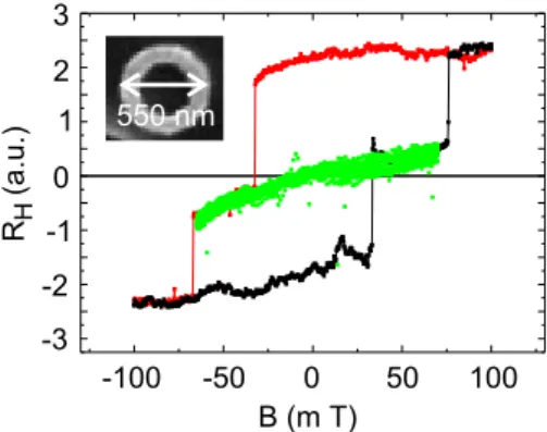
history, is removed in case of sample (III). In Fig. 4 we show the Hall effect in a mesoscopic 2DES which was beneath a permalloy nanoring. Here, mainly two magnetic config-urations are distinguished: firstly, at high positive field the nanoring is in the so-called onion state [24] where both arms are magnetized in the same direction along the applied field. Secondly, close to zero field the ring is expected to be in a circular state, i.e., the microscopic magnetic moments are aligned in a ring-shaped fashion. If we reverse the magnetic field before the irreversible jump to the opposite onion state occurs, we find that the measured Hall voltage in the rema-nent state remains in the center of the hysteretic trace.
In the scenario of the ring-shaped magnetization state, the stray field of the nanoring vanishes in zero magnetic field since, if compared to the nanodisk, the perpendicular vortex is no longer present.
4
Conclusion
We have shown that the magnetic behavior of permalloy nanostructures is governed by the shape. In case of ring-shaped nanomagnets the stray-field effects in the remanent state can be vanishingly small. Our findings might be help-ful for the design of ferromagnetic contacts in lateral fer-romagnet/semiconductor valve devices in future spin-injection experiments.
Acknowledgements
D. Grundler thanks E. A. de Andrada e Silva for his very kind hospitality during the stay at INPE in Sao Jose dos Campos and FAPESP and DAAD for the financial support. The work has been supported by the DFG via He1938/9 and via the Graduiertenkolleg ’Nanostrukturierte Festk¨orper’.
Figure 4. Local Hall effect measured in a mesoscopic 2DES at 4.2 K which was beneath a permalloy nanoring with an outer di-ameter of 550 nm and an inner didi-ameter of 300 nm. An offset is subtracted from the curves such that the absolute Hall voltage at maximum positive and minimum negativeBis the same. The in-ner data reflect several up and down sweeps where the fieldBis always between the switching fields to the saturated onion states. Data taken from Ref. [25].
We gratefully acknowledge continuous support of our work by D. Heitmann, experimental help by N. Klockmann and MBE growth of the semiconductor heterostructures by Ch. Heyn.
References
[1] S. Datta and B. Das, Appl. Phys. Lett.56, 665 (1990) [2] D.D. Awschalom, M.E. Flatte and N. Samarth, Sci. Am.286,
66 (2002)
[3] D. Grundler, Phys. World15(no. 4), 39 (2002)
[4] G. Meier and D. Grundler, inFestk¨orperprobleme - Advances in Solid State Physics/Vol. 40, Ed. B. Kramer (Braunschweig: Vieweg 2000) p 295; and references therein
[5] S.A. Wolfet al., Science294, 1488 (2001); and references therein
[6] P. Hammar, B.R. Bennett, M.J. Yang, and M. Johnson, Phys. Rev. Lett.83, 203 (1999); Phys. Rev. Lett.84, 5024 (2000) [7] A.T. Filip, B. H. Hoving, F. J. Jedema, B.J. van Wees, B.
Dutta, and S. Borghs, Phys. Rev. B62, 9996 (2000) [8] F.G. Monzon, H.X. Tang, and M.L. Roukes, Phys. Rev. Lett.
84, 5022 (2000)
[9] B.J. van Wees, Phys. Rev. Lett.84, 5023 (2000)
[10] J.-I. Inoue, G.E. Bauer, and L.W. Molenkamp, Phys. Rev. B
67, 033104 (2003); and references therein [11] D. Grundler, Phys. Rev. Lett.86, 1058 (2001) [12] D. Grundler, Phys. Rev. B63, R161307 (2001)
[13] T. Matsuyama, C.-M. Hu, D. Grundler, G. Meier, and U. Merkt, Phys. Rev. B65, 155322 (2002)
[14] O. Wunnicke, Ph. Mavropoulos, R. Zeller, P.H. Dederichs, and D. Grundler, Phys. Rev. B65, 241306(R) 2002. [15] A. Geim, S. V. Dubonos, J. G. S. Lok, I. V. Grigorieva, J. C.
Maan, L. Theil Hansen, and P. E. Lindelof, Appl. Phys. Lett.
Dirk Grundleret al. 601
[16] G. Meier, D.Grundler, K.-B. Broocks, Ch. Heyn, and D. Heit-mann, JMMM210, 138 (2000).
[17] Y. Takagakiet. al., Solid State Comm.68, 1051 (1988). [18] G. Meier, M. Halverscheid, T. Matsuyama, and U. Merkt, J.
Appl. Phys.89, 7469 (2001).
[19] G. Prinz, US patent 5,542,868 and US patent 6,381,170. [20] D. Grundler, T. M. Hengstmann, N. Klockmann, Ch. Heyn,
and D. Heitmann, Physica E12, 248 (2002).
[21] T. M. Hengstmann, D. Grundler, N. Klockmann, H. Rolff, Ch. Heyn, and D. Heitmann, IEEE Trans. Magn. 38, 2535 (2002).
[22] R.P. Cowburnet al., Phys. Rev. Lett.83,1042 (1999). [23] T.M. Hengstmann, D. Grundler, Ch. Heyn, and D. Heitmann,
J. Appl. Phys.90, 6542 (2001).