894 Brazilian Journal of Physics, vol. 36, no. 3B, September, 2006
Inverse Photoemission Spectroscopy of Multiwall Carbon Nanotubes
Samuel Hevia1,2, Wladimir Ib´a˜nez1, Rodrigo Segura1, and Patricio H¨aberle1
1Departamento de F´ısica, Universidad T´ecnica Federico Santa Mar´ıa, Avenida Espa˜na 1680, Valpara´ıso, Chile 2Instituto de F´ısica, Universidad Cat´olica de Valpara´ıso, Av. Brasil 2950, Valpara´ıso, Chile
Received on 04 December, 2005
Multiwall Carbon Nanotubes (MWCNTs) were synthesized by Chemical Vapor Deposition (CVD). Two dif-ferent procedures were used to grow MWCNT films roughly, aligned in the direction normal to the SiO2/Si(111)
substrate. Inverse Photoemission Spectroscopy measurements, on these samples, show the existence of reso-nances which could be traced back to a flat graphene sheet. The unoccupied valence band is fairly similar to that shown by graphite except by an additional intensity in the vicinity of theFermilevel. This resonance could be interpreted both as tubes tips end effects orvan Hovesingularities in the density of states.
Keywords: Multiwall carbon nanotubes; Inverse photoemission
I. INTRODUCTION
In the last few years an important number of scientists from different disciplines have concentrated their efforts in the field of nanoscale materials science and technology. In particu-lar, the study of Carbon Nanotubes (CNTs) properties has attracted a special interest. Applications like field emitters, diodes, transistors, flat-panel displays, SPM tips, hydrogen storage, reinforced polymers and molecular delivery are only a few of their possible applications.
Photoemission experiment [1] have demonstrated the occu-pied electronic structure of MWCNTs arrays is similar to that of highly ordered pyrolytic graphite (HOPG). The main dif-ferences are found in the existence of resonances very close to theFermiedge[1]. In SWCNT these states were attributed tovan Hovesingularities of the density of states (DOS). Due to the additional quantization along the nanotube circumfer-ence, peaks appear symmetrically around theFermilevel (εF) and their energy splitting depends mainly in the diameter of the tubes. In the case of MWCNTs the nature of these ad-ditional intensities close toFermi level is still controversial. They have been attributed to emissions from the tubes tips [2] or to resonances derived from a mixture of theπbands and the 1D subband of the nanotubes [3].
It is well known that CNTs can be grown by Chemical Va-por Deposition (CVD) methods, by nucleation of C around metallic particles of Fe, Co and Ni [4]. Nanoparticles of these metals act as catalyst in the decomposition of hydrocarbon-ated molecules such as methane, ethane or acetylene.
In this work we used two CVD procedures in order to synthesize aligned MWCNT-films on flat SiO2/Si(111) sub-strates. One of the films was obtained by pyrolysis of Iron (II) Phthalocyanine [5]. This compound has a double func-tion, first supplying iron atoms for the formation of the cat-alytic nanoparticles and then as a carbon source. In the other method pyrolysis of acetylene over nanostructured Fe films was used [6]. Most of the previous measurements of the elec-tronic structure of these systems have been done on states be-lowεF and there is not much information on the empty elec-tronic states. Consequently the aim of this paper is to de-scribe the electronic structure of unoccupied states of MWC-NTs, aboveεFusing IPS.
II. EXPERIMENTAL SECTION
Multiwall Carbon Nanotubes were synthesized by Thermal Chemical Vapor Deposition (CVD) in a horizontal tube fur-nace (4.5 cm inner diameter).
Growth method I:(sample I) This procedure has been pre-viously reported [5]. In a typical reaction, 0.05g of Fe-Pc were decomposed over SiO2/Si(111) wafers at 1000oC. The reac-tion under these condireac-tions takes about 20 min.
Growth method II:(sample II) Previous to the introduc-tion in the furnace, Fe thin films were electron beam evap-orated onto SiO2/Si(111) [6]. The coverage of the iron films was estimated by Auger Electron Spectroscopy (AES) to be 60% atomic abundance. The post-treatment annealing (800oC×20 min, in the CVD furnace) of this film in the presence of hydrogen, induces the formation of Fe nanostruc-tures (np-Fe). The CNT growth was carried out by catalytic decomposition of acetylene, at 800oC, for half an hour.
Scanning Electron Microscopy (SEM) micrographs were obtained from the as prepared samples, in a LEO SEM 1420VP. Transmission Electron Microscopy (TEM) measure-ments were performed over dispersed samples. The micro-graphs were taken in a Zeiss EM900 operated at 80 KV.
Inverse photoemission spectroscopy (IPS) has been used to obtain information regarding the unoccupied density of states. The signal corresponds to the intensity of photons emitted by a sample bombarded by low energy electrons. In a process much like the generation of X-rays, Vacuum Ultravi-olet (VUV) photons are created by an electronic transition in the solid. The intensity of emitted photons is closely depen-dent on the unoccupied density of states (uDOS). Measure-ments were performed in a home built isochromat spectrome-ter [7].
III. RESULTS
Samuel Hevia et al. 895
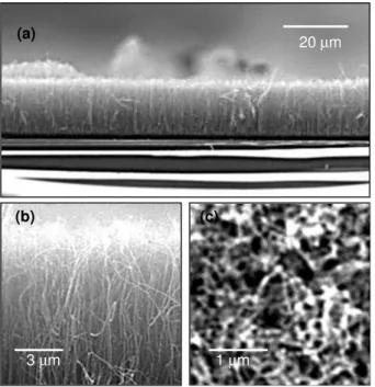
Figure 1 shows a series of SEM micrographs of a CNT film grown by pyrolysis of Iron Phthalocyanine (sample I). Figure 1(a), shows the side view of a 18µm thick CNT-film. Figures 1(b) and 1(c) are a magnification of the lateral profile and the top view, respectively.
Figure 2 shows the SEM micrographs of a CNT array grown by pyrolysis of acetylene over an annealed 60%-iron film (sample II). The thickness of the CNT-film estimated from figure 2(a) is 82µm. Figures 2 (a), 2(b) and 2(c) cor-respond to the same views shown in Fig. 1.
Transmission electron micrographs of dispersed tubes were also analyzed. For sample I, the mean diameter was 56 nm whereas for sample II the mean diameter was 49 nm.
From the SEM and TEM micrographs it is possible to verify some differences between samples I and II. The first one is the film thickness, as has been described above. Additionally, sample I presents straight tubes whereas CNTs in sample II have a helical structure.
From the top view it can be verified that although the MWCNT-films show a good microscopic order, most of the tube tips on the top of the film are bended with a random ori-entation in the plane.
Figure 3 a) shows normal incidence IP spectra of samples I and II taken over a wide energy range. The energies are measured with respect to the Fermi level, value which is fixed using normal incidence IP spectra from an Al sample. The main features in both spectra have been labeled A and A’, they are both close to 3[eV] but with a clear shift in energy between both samples, indicating some electronic structure differences between the samples. B’ and B are broad resonances located close to an energy of 12,5[eV].
fixed using IP spectra from an Al sample. Traces I and II
(c) (b)
(a) 20 µm
3 µm 1 µm
µ
FIG. 1: SEM images of MWCNTs film synthesized by Fe-Pc pyrol-ysis over a SiO2substrate. (a) and (b) lateral views; (c) top view.
With the idea of comparing the electronic structure MWC-NTs with other systems, in figure 2(b) we present three
spec-(c) (b)
(a)
20 µm
3 µm 1 µm
FIG. 2: SEM images of CNTs synthesized from acetylene decompo-sition over 60%-Fe/SiO2. Note the helicoidal symmetry of the tubes.
(a) and (b) lateral views; (c) top view.
tra, from the top: a sputtered HOPG sample, MWCNT ple II and data from a fresh HOPG surface. This last sam-ple has two resonances C and D in this energy range. Reso-nance C, at about 1.8 eV, has been identified as theπ* band [8] and D as the n=1 surface image state [9] of graphite. The dominant feature in the CNTs sample is resonance A at 3.2 [eV]. An additional, less intense feature (C’) is detected at 1.7 [eV]. Sputtered HOPG shows a very broad feature (approxi-mately 2[eV]) centered around 1.2 [eV], raising the IPS inten-sity closer toεFwhen compared to the fresh HOPG surface.
896 Brazilian Journal of Physics, vol. 36, no. 3B, September, 2006
IV. DISCUSSION
The general belief, at least for large diameter nanotubes, is that most of the electronic structure of Carbon Nanotubes could be traced back to the two-dimensional material from which they are constructed, graphene. This single atomic layer of graphite consists of a 2-D honeycomb structure of σsp2-bonded carbon atoms. The in plane bonding (σorbitals) form strong covalent bonds with neighboring carbon atoms. Therefore, occupiedσand unoccupiedσ* bonds are formed. The third C 2p electrons are in 2pz-orbitals perpendicular to the plane and form a weakerπbond with the 2pz-orbitals of the atoms in neighboring sites. Due to a weaker bonding, the splitting between the occupied and the unoccupiedπbands is smaller, thus theπ* band appears closer toεF.
Photoemission spectra from CNTs are dominated by emis-sion fromπandσbands with resonances at 3[eV] and 8[eV] belowεF respectively [2]. One of the main differences with graphite is the extra emission close toεF, which has been ob-served on SWCNTs, MWCNTs and even in more complex carbon “onions” like structures [10]. On SWCNTs, the pho-toemission data show clear oscillations in the density of states, in agreement with theoretical predictions based of van Hove singularities of the DOS. For MWCNTs this increased inten-sity has been explained in two ways. Suzuki et al. [2] using photoelectron spectro-microscopy have studied the valence band structure along a single tube axis. Their spectra showed an increased intensity atεFonly from the spatial region close to the top of the tubes. They explain this behavior as struc-tural defects of the tube tips by the insertions of pentagons on the graphene network, hence implying a higher density of dangling bond at the spherical tips than in the cylindrical side walls. On the other hand Choi et al.[3] using photoemission and density functional calculations postulate the additionalεF intensity is due to mixing between π bands and a truly 1D subband between layers.
If the behavior of the unoccupied valence band in CNTs is similar to the occupied states, as expected, the resulting spec-tra should resemble those obtained from graphite.
Figure 3(b) shows the IPS spectra from HOPG. Two are the dominant features, one at 1.8[eV] aboveεF which corre-sponds to the non dispersingπ∗band resonance and the image state at 3.5[eV]. For HOPG no increased intensity is observed close toεF. When we compare the graphite spectra with the one from the MWCNT sample, we can observe a small shoul-der in the emission which seems to be related to theπ∗bands, with an obvious reduction in the intensity. Nevertheless this feature is always present in all collected spectra with a small fluctuation in energy as we change to different places in the sample, but it remains unchanged within the resolution of the spectrometer. Above 3.5 [eV] we only detect one reproducible structure, in each sample, around 12.5 [eV], (B and B’). By comparing to graphite the energy of this fairly broad reso-nance corresponds to theσ* band. Probably the most signif-icant departure with HOPG is the complete disappearance of the image resonance D, which by the very nature of this state, it requires of a flat surface to exist. If this type of state exists in CNTs the symmetry of the tubes must induce a shift in the
Samuel Hevia et al. 897
energy of the resonance. The idea of collecting spectra from a sputtered HOPG was done to compare the effects of gen-erating many defects on the HOPG surface with the disorder induced states in the NT’s spectra. There are two important effects on HOPG: the complete disappearance of resonance D, as expected, and the increased intensity (E) in the IP spec-trum close toεF. These extrinsic surfaces states, which are linked to disorder, have a higher contribution to the DOS for energies of the order of 1 [eV] and below. In fact, this result is consistent with the difficulties we had in getting a low noise measurement in CNTs samples close toεF. Most likely this noise was due to e-beam induced damage of the tubes, hence the need of lowering the dose. Even though both helical and straight tubes are fairly well aligned with the substrate nor-mal, we see no angular dependence of the IPS intensity of any feature. This result together with the SEM images of top of the film led us to believe we only have access to the tips of the tubes or whatever tubes are lying in the top of the CNT film. In both cases no dependence in the orientation of the e-beam
is expected. Resonances A and A’ could be related to band structure effects of the tubes, but further measurements are re-quired to clarify this point, since the energy of the resonances could be linked to the tube diameter.
For resonance F, which appears robustly in CNT samples, we could not narrow down, to a single one, the justification for the origin of this feature. Two competing explanations are: the resonance is linked to dangling bonds at the tip of the tubes; or the 1D nature of the tubes DOS, which can manifest itself even at these very large tube diameters. This is clearly an open question, which with the information available to us now, can not be resolved.
Acknowledgement
SH thanks CONICYT for his Doctoral Fellowship. RS thanks MECESUP for his Postdoctoral Fellowship. Partial funding for this research has been provided by Fondecyt, and MSI-Condensed Matter Physics Nucleus (PO2-054-F), Chile.
[1] H. Ishii, H. Kataura et al., Nature426, 540 (2003).
[2] S. Suzuki, Y. Watanabe, T. Ogino S. Heun et al, Phys. Rev. B 66, 35414 (2002).
[3] J. Choi, S. Lee, Y. Choi, Y. Lee, and J. Jiang, Chem. Phys. Lett 349, 185. (2001).
[4] C. J. Lee, J. Park, Y. Huh, and J. Y. Lee, Chem. Phys. Lett.343, 33 (2001); S. Takenaka, M. Ishida, M. Serizawa, E. Tanabe, and K. Otsuka, J. Phys. Chem. B108, 11464 (2004); M. Paillet, V. Jourdain, P. Poncharal, J. L. Sauvajol, A. Zahab, J. C. Meyer, S. Roth, N. Cordente, C. Amiens, and B. Chaudret, J. Phys. Chem. B108, 17112 (2004).
[5] R. A. Segura, W. Ib´a˜nez, R. Soto, and P. H¨aberle, J. Nanosci.
Nanotech.6, 1945 (2006).
[6] R. A. Segura, M. Flores, P. H¨aberle, in prep.
[7] P. H¨aberle, W. Iba˜nez, R. Esparza, and P. Vargas, Phys. Rev. B63, 235412 (2001).
[8] B. Reihl, J. K Gimzenski, J. M. Nicholls, and E. Tosatti, Phys. Rev. B33, 5770 (1986).
[9] I. R. Collins, P. T. Andrews, and A. R. Law, Phys. Rev. B38, 13348 (1988).