Setembro , 2016
Duarte Miguel Ribeiro Guerra
Licenciado em Ciências da Engenharia Electroté cnica e de Computadores
Advanc ed Elec tric al Charac terizatio n o f Oxide TFTs
Design o f a Temperature Co mpensated Vo ltage
Referenc e
Dissertação para obtenção do Grau de Mestre em
Engenharia Electroté cnica e de Computadores
Orientador: Asal Kiazadeh,
Professora Doutora, Universidade Nova de Lisboa
Co -orientadores: João Carlos da Palma Go es,
Professor Douto r, Universidade Nova de Lisboa
Pedro Miguel Cândido Barquinha,
Professor Douto r, Universidade Nova de Lisboa
Júri:
Presidente : Prof. Doutor Luís Filipe dos Santos Gomes, FCT-UNL
Argue nte: Prof. Doutor Vítor Manue l Grade Tavares, FEUP
Vogais: Prof. Doutor João Carlos da Palma Goes, FCT-UNL
Advanced Electrical Characterization of Oxide TFT’s
Copyright © Duarte Miguel Ribeiro Guerra, Faculdade de Ciências e Tecnologia, Universidade Nova de Lisboa.
v
vii
Agradecimentos
Antes dos capítulos relativos à apresentação e explanação da presente tese, deixo um especial agradecimento aos meus caros professores e orientadores, nomeadamente, a professora Asal Kiazadeh, o professor João Goes e o professor Pedro Barquinha, por me terem ajudado e acompanhado pacientemente durante os últimos meses, a fim da realização deste projecto, sempre prontos a receberem-me nas suas horas vagas. Desta forma, encontraram-se sempre presentes, o que resultou também, numa motivação extra para a conclusão da mesma, mostrando-se mostrando-sempre disponíveis e prontos a esclarecer quaisquer dúvidas ou problemas.
Dito isto, quero deixar também um especial agradecimento à Faculdade de Ciências e Tecnologias da Universidade Nova de Lisboa por me ter ajudado a crescer nos últimos anos, quer como pessoa, quer como futuro engenheiro, nas mais variadas vertentes, tais como interpessoais, culturais, entre outras.
Não posso deixar de frisar que a minha chegada até ao ponto em que me encontro hoje não teria sido possível sem o permanente apoio dos meus pais, que sempre prezaram e investiram na minha educação, tal como não posso deixar de mencionar a minha estimada irmã, parte integrante dos meus últimos dezassete anos de vida, e sempre se encontrou ao meu lado.
viii
ix
Abstract
Any electronic device, regardless of its function, needs a reference voltage source that feeds reliably, i.e., which generates a constant voltage, upstream and regardless of external environmental conditions, such as temperature. Since such a characteristic negatively influences the behavior of the devices, whose base el-ements are transistors, it is essential to design a circuit that provides a voltage which is invariant over a temperature range.
In this work is designed a circuit that is responsible for generating a refer-ence voltage using only thin film transistors or TFTs, on glass substrate. How-ever, in order to validate the concept used in the mentioned transistors, it is also dimensioned and simulated the proposed circuit in 130 nm CMOS technology, where the respective results are expected to be comparative between the two technologies. For CMOS technology, for a nominal reference voltage of 124,0 mV, Cadence simulation reveals ±2,2 ppm/ºC temperature coefficient, between -20 °C and 100 °C. The power consumptions are and 1,434 mW and 4,566 mW for both CMOS and IGZO-TFT technologies, respectively.
xi
Resumo
Qualquer dispositivo electrónico, independentemente da sua função, neces-sita sempre de uma fonte de tensão de referência que o alimente de forma fiável, isto é, que gira uma tensão constante, a montante, e independente de condições externas do meio, tal como a temperatura. Visto que a referida característica in-fluencia negativamente o comportamento dos dispositivos, dado que têm como elemento base o transístor, é essencial projectar um circuito que, à sua saída, for-neça uma tensão invariante ao longo de uma escala de temperatura.
Neste trabalho é dimensionado um circuito responsável por gerar uma ten-são de referência, utilizando apenas transístores de película fina, ou TFTs (Thin Film Transistors), em substrato de vidro. Contudo, a fim de se validar o conceito utilizado nos referidos transístores, é também dimensionado e simulado o cir-cuito proposto em tecnologia CMOS 130 nm, onde se obtêm também resultados que vêm a ser comparativos entre ambas as tecnologias. Em tecnologia CMOS, para uma tensão de referência de 124,0 mV, as simulações em Cadence revelam um coeficiente de temperatura de ±2,2 ppm/ºC, entre -20ºC e 100ºC. As potências consumidas são de 1,434 mW e 4,566 mW para as tecnologias CMOS e TFTs IGZO, respectivamente.
xiii
Contents
AGRADECIMENTOS ... VII
LIST OF TABLES ... XVII
LIST OF FIGURES ... XV
ABBREVIATIONS ... XIX
1. INTRODUCTION ... 1
1.1. BACKGROUND AND MOTIVATION ... 1
1.2. THESIS ORGANIZATION ... 2
1.3. CONTRIBUTIONS ... 3
2. INDIUM-GALLIUM-ZINC-OXIDE TFT ... 5
2.1. INTRODUCTION ... 5
2.2. TFT STRUCTURES ... 7
2.3. BASIC CHARACTERISTICS ... 9
2.4. ELECTRICAL PARAMETER EXTRACTION ... 10
2.4.1. Threshold Voltage ... 10
2.4.2. Charge Carrier Mobility ... 12
2.4.3. Capacitance per unit area ... 12
3. LOW-VOLTAGE REFERENCE TOPOLOGIES ... 15
3.1. INTRODUCTION ... 15
3.2. BANDGAP REFERENCE CIRCUIT ... 15
3.3. ALOW-VOLTAGE CMOSVOLTAGE REFERENCE BASED ON PARTIAL COMPENSATION OF MOSFETTHRESHOLD VOLTAGE AND MOBILITY USING CURRENT SUBTRACTION ... 18
xiv
3.5. CONCLUSIONS ... 31
4. DESIGN METHODOLOGY AND ELECTRICAL SIMULATIONS USING A STANDARD 130 NM TECHNOLOGY ... 33
4.1. INTRODUCTION ... 33
4.2. MATHEMATICAL ANALYSIS ... 34
4.3. SIMULATION RESULTS ... 43
4.4. CONCLUSIONS ... 48
5. DESIGN METHODOLOGY AND ELECTRICAL SIMULATIONS USING TFTS ON GLASS 49 5.1. INTRODUCTION ... 49
5.2. PROPOSED CIRCUIT ... 49
5.3. DESIGNING-FOR-TESTING FLEXIBILITY ... 51
5.3.1. NOT Gate ... 51
5.3.2. NAND Gate ... 52
5.3.3. 3x8 Decoder ... 53
5.4. SIMULATION RESULTS ... 54
5.4.1. Proposed Circuit Results, Using a Standard 130 nm Technology ... 55
5.4.2. DIGITAL LOGIC RESULTS ... 57
5.4.3. Proposed Circuit Results, using TFTs on Glass Technology ... 59
6. CONCLUSIONS AND FUTURE WORK ... 63
xv
List of Figures
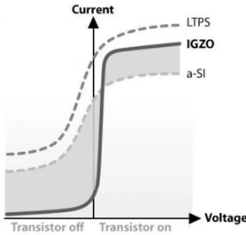
FIGURE 2.1:DEMONSTRATIVE COMPARISON OF I-V CHARACTERISTICS BETWEEN A-SI,IGZO AND LTPSTFTS. ... 7
FIGURE 2.2:GENERAL TFT STRUCTURES: A)STAGGERED BOTTOM-GATE; B)COPLANAR BOTTOM-GATE; C) STAGGERED TOP-GATE; D)COPLANAR TOP-GATE. ... 9
FIGURE 2.3:CURRENT-VOLTAGE CHARACTERISTIC OF A GENERIC TRANSISTOR. ... 10
FIGURE 2.4:VTH EXTRACTION, USING LINEAR EXTRAPOLATION METHOD.NOTE:VTH IS EXPRESSED AS VT [7]. ... 11
FIGURE 2.5:ACCUMULATION CHARGE DENSITY AS A FUNCTION OF THE APPLIED GATE VOLTAGE [12]... 13
FIGURE 3.1:GENERIC REPRESENTATIONS OF: A)PTAT REFERENCE; B)CTAT REFERENCE. ... 16
FIGURE 3.2:SIMPLE BGR CIRCUIT. ... 17
FIGURE 3.3:SIMPLE BGR CIRCUIT, WITH TWO NPN TRANSISTORS IN DIODE-CONFIGURATION WITH DIFFERENT WIDTHS. ... 18
FIGURE 3.4:CMOS BIAS CIRCUIT REPORTED BY [14]. ... 19
FIGURE 3.5:CURRENTS SUBTRACTION SCHEME, REPORTED BY [1]. ... 22
FIGURE 3.6:PROPOSED VOLTAGE REFERENCE REPORTED BY [1]. ... 23
FIGURE 3.7:THE TRADITIONAL BANDGAP VOLTAGE REFERENCE CIRCUIT REALIZED IN CMOS TECHNOLOGY WITH PARASITIC VERTICAL PNP BIPOLAR JUNCTION TRANSISTORS [18]. ... 28
FIGURE 3.8:THE IMPLEMENTATION OF THE NEW PROPOSED BANDGAP VOLTAGE REFERENCE CIRCUIT WITH ALL TFT DEVICES IN A LTPS PROCESS [18]. ... 30
FIGURE 4.1:CIRCUIT TO EXTRACT THE NEEDED PARAMETERS OF A NMOS TRANSISTOR. ... 35
FIGURE 4.2:SIMULATION OF VTH OVER TEMPERATURE OF THE NMOS TRANSISTOR. ... 36
FIGURE 4.3:SIMULATION OF VTH OVER TEMPERATURE OF THE PMOS TRANSISTOR. ... 36
FIGURE 4.4:SIMULATION OF KN OVER TEMPERATURE OF THE NMOS TRANSISTOR. ... 37
FIGURE 4.5:SIMULATION OF KP OVER TEMPERATURE OF THE PMOS TRANSISTOR. ... 38
xvi
FIGURE 4.7:TEMPERATURE CHARACTERISTICS OF VCTAT2, FROM 273K TO 373K.THE BLACK LINE REPRESENTS
THE SIZE RELATION (W/L)=(10 µM/1 µM). ... 41
FIGURE 4.8:I1 CURRENT GENERATOR. ... 43
FIGURE 4.9:VCTAT1 VOLTAGE BEHAVIOR FOR DIFFERENT VALUES OF R1, IN STEPS OF 5 KΩ, FROM 20 KΩ TO 50 KΩ. THE YELLOW MARKED LINE REPRESENTS THE CHOSEN VALUE FOR R1=25 KΩ. ... 44
FIGURE 4.10:I1 CURRENT BEHAVIOR FOR DIFFERENT VALUES OF R1, IN STEPS OF 5 KΩ, FROM 20 KΩ TO 50 KΩ.THE PINK MARKED LINE REPRESENTS THE CHOSEN VALUE FOR R1=25 KΩ. ... 44
FIGURE 4.11:I2 CURRENT GENERATOR. ... 45
FIGURE 4.12:VCTAT2 VOLTAGE BEHAVIOR FOR DIFFERENT VALUES OF R2, IN STEPS OF 10 KΩ, FROM 150 KΩ TO 200 KΩ.THE BLUE MARKED LINE REPRESENTS THE CHOSEN VALUE FOR R2=180 KΩ. ... 45
FIGURE 4.13:I2 CURRENT BEHAVIOR FOR DIFFERENT VALUES OF R2, IN STEPS OF 10 KΩ, FROM 150 KΩ TO 200 KΩ. THE ORANGE MARKED LINE REPRESENTS THE CHOSEN VALUE FOR R2=180 KΩ. ... 46
FIGURE 4.14:OUTPUT VOLTAGE OF THE CIRCUIT WITH A PARAMETRIC ANALYSIS OF THE SIZE OF THE WIDTH OF THE TRANSISTOR T7, WHICH TOOK VALUES OF 46µM,47µM AND 48µM, FOR THE CURVES IN YELLOW, GREEN AND BLUE, RESPECTIVELY. ... 47
FIGURE 5.1:PROPOSED CIRCUIT USING ONLY N-TYPE CHANNEL TRANSISTORS. ... 50
FIGURE 5.2:INVERTER CIRCUIT, USING N-TYPE TRANSISTORS. ... 52
FIGURE 5.3:NAND CIRCUIT, USING N-TYPE TRANSISTORS. ... 52
FIGURE 5.4:DECODER CIRCUIT, USING NOT AND NAND GATES SPECIFIED IN FIGURES 5.2 AND 5.3. ... 54
FIGURE 5.5:CURRENT CHARACTERISTICS OVER TEMPERATURE: A)I1, FOR R1=60 KΩ; B)I2, FOR R2=800 KΩ. ... 55
FIGURE 5.6:PARAMETRIC ANALYSIS OF THE OUTPUT VOLTAGE FOR DIFFERENT WIDTH SIZES.THE GREEN CURVE ON TOP REPRESENTS THE OUTPUT VOLTAGE FOR W=20 µM. ... 56
FIGURE 5.7:NOT GATE OUTPUT SIGNAL. ... 57
FIGURE 5.8:NAND GATE OUTPUT SIGNAL. ... 57
FIGURE 5.9:DECODER OUTPUT SIGNAL FOR EACH COMBINATION OF THE INPUTS. ... 58
FIGURE 5.10:NOT GATE LAYOUT. ... 60
FIGURE 5.11:NAND GATE LAYOUT. ... 60
FIGURE 5.12:3-BIT DECODER LAYOUT. ... 60
FIGURE 5.13:FINAL TFT CIRCUIT LAYOUT, WITH ANALOG AND DIGITAL CIRCUITS INTEGRATED. ... 61
xvii
List of Tables
TABLE 4.1:TECHNOLOGY PARAMETERS. ... 34
TABLE 4.2:TRANSISTOR SIZES. ... 34
TABLE 4.3:THRESHOLD VOLTAGE VARIATION OVER TEMPERATURE OF NMOS AND PMOS TRANSISTORS OF A 130 NM TECHNOLOGY. ... 37
TABLE 4.4:CONDUCTION PARAMETER VARIATION OVER TEMPERATURE OF NMOS AND PMOS TRANSISTORS OF A STANDARD 130NM TECHNOLOGY. ... 38
TABLE 4.5:THICKNESS OXIDE PARAMETERS OF NMOS AND PMOS TRANSISTORS OF A 130 NM TECHNOLOGY... 39
TABLE 4.6:CAPACITANCE PER UNIT AREA OF NMOS AND PMOS TRANSISTORS OF A STANDARD 130 NM TECHNOLOGY. ... 39
TABLE 4.7:ELECTRON’S MOBILITY OVER TEMPERATURE OF NMOS AND PMOS TRANSISTORS OF A STANDARD 130 NM TECHNOLOGY. ... 40
TABLE 4.8:OVERALL THEORETICAL RESULTS. ... 48
TABLE 4.9:OVERALL SIMULATION RESULTS. ... 48
TABLE 5.1:TRUTH TABLE OF THE INVERTER... 52
xix
Abbreviations
ADC Analog to Digital Converter
AMOLED Active-Matrix Organic Light-Emitting Diode
a-Si Amorphous Silicon
BGR Bandgap Voltage Reference
BJT Bipolar Junction Transistor
CMOS Complementary Metal-Oxide-Semiconductor
CTAT Complementary to Absolute Temperature
DAC Digital to Analog Converter
IGZO Indium-Gallium-Zinc-Oxide
KCL Kirchhoff Current Law
LCD Liquid Crystal Display
LTPS Low Temperature Polycrystalline Silicon
MOSFET Metal Oxide Semiconductor Field Effect Transistor
NMOS N-Channel MOSFET Transistor
xx
OLED Organic Light-Emitting Diode
PCB Printed Circuit Board
PMOS P-Channel MOSFET Transistor
PNP Positive-Negative-Positive
Poly-Si Polycrystalline Silicon
PTAT Proportional to Absolute Temperature
SFDR Spurious Free Dynamic Range
SMD Surface-Mount Device
SRAM Static Random Access Memory
Ta2O5 Tantalum Pentoxide
TC Temperature Coefficient
TFT Thin-Film Transistor
1
1.
Introduction
1.1.
Background and Motivation
So far, transistors have been the main component of every integrated circuit. Nowadays, a single processor, can take billions of these components in a very small area and this can lead to an increase of generated heat, which can result in several problems, such as system instability. This happens because the behavior of the transistors changes, in general, according to the temperature. Assuming that transistors are not ideal components and the circuits where they are fitted need to be powered reliably, the design of a stable voltage reference within a large temperature range is crucial. An ideal voltage reference has no variation, which means that independently of the temperature, the value of its output is always the same which is the objective of this work.
There are several types of transistors with different configurations that combine the positions of their different layers, as well as the respective materials. Considering this, the motivation of this work is to design a low-voltage reference circuit using only thin film transistors and comparing the obtained results with a standard technology, such as CMOS 130 nm. Although, despite the number of different material combinations that can be used, the TFTs in question are made of amorphous Indium-Gallium-Zinc-Oxide, also known as IGZOs. They have several advantages when compared to Zinc-Tin-Oxide of amorphous Silicon TFTs, such as higher mobility and simpler fabrication processes.
2
To master the technique of designing a reliable voltage reference, a first study is made of the concept used in [1]. It is also described and validated, using CMOS 130 nm along mathematical and simulation resources, like MathCAD and Spectre, and then a different circuit is proposed and tested, using only glass-TFTs, which has never been done.
1.2.
Thesis Organization
The present work is organized in six main chapters that are briefly de-scribed below, with the exception of the introductory one.
Chapter 2 introduces IGZO TFTs, describing what are the principal modes of operation, what types of structures are mainly used, as well as their principal differences, and a comparison between different materials that compose them.
Chapter 3 is about low-voltage reference topologies. In this chapter several topologies are analyzed theoretically, including the one that is used as base for this work.
Chapter 4 includes all the work that was made in CMOS 130 nm technology, starting from initial considerations, theoretical analysis and how the starting point was calculated to the final results and simulations. All steps from the initial circuit from [1] are described to an end where only n-type channel transistors are used with the same physical dimensions as TFTs, which leads to the next chapter. Chapter 5 describes the methodology and presents the results of the respec-tive simulations when using real TFTs since it was not possible to test them by software simulations because the respective models were not characterized in temperature.
3
1.3.
Contributions
Thin-film transistors differ from other more traditional types of transistors because they have the ability of being implemented on transparent substrate ma-terials, being glass or plastic good examples of those. This leads to a new world of electronic implementation ideas, like electronic papers that can be bent, curved displays, completely transparent devices, and many others. For this to be appli-cable, all of the transistors need to have the same substrate, including, in the pre-sent case, the voltage reference module. However, the thermal characteristics of IGZOs, which are essential to develop a viable low-voltage reference, are not fully understood. Therefore, this work addresses that problem and helps to un-derstand and develop a reliable voltage reference module, with a very low-voltage variation across the entire operational temperature variation, from -20ºC to 100ºC.
5
2.
Indium-Gallium-Zinc-Oxide TFT
2.1.
Introduction
Thin-film transistors are most commonly used in smartphone displays. These transistors are responsible for turning the individual pixels ‘on’ and ‘off’. This type of application requires efficient and low powered technologies. How-ever, there are many more TFT applications, such as high density SRAMs, non-volatile memories, photo detector amplifiers, thermal printer heads, image sen-sors of finger print sensen-sors.
There are many different TFT structures, fabrication processes, electrical characteristics, design parameters and physical materials that have to be consid-ered in order to achieve the final objective and they are described in the present chapter.
Despite the fact that a single display can have multiple layers, usually five or more, it can be divided in two main categories, which are the backplane and the light emitting materials. Considering the first one, there are numerous tech-nologies that can be used. However, major techtech-nologies use the following three types of materials, which are amorphous-Silicon, Indium-Gallium-Zinc-Oxide and Low Temperature Polycrystalline Silicon. As light emitting material types, the most commonly used are LCDs, OLEDs and, the most recent, AMOLEDs.
6
Amorphous Silicon has been the go-to material for backplane technology for many years and with a variety of different manufacturing methods, always with the objective of improving energy efficiency, refresh speeds and display’s viewing angle. Due to the physical limitations of this material, the number of pixels per inch has to be limited to around 300, not being suitable on higher end AMOLED displays, since they put more electrical stress on the transistors, which a-Si TFTs cannot handle. That is where LTPS and IGZO come in. As a great ad-vantage, a-Si TFTs are very cheap and have relatively simple manufacturing pro-cesses.
Low temperature polycrystalline silicon TFTs have higher temperature pro-cess manufacturing than a-Si TFTs (approximately 650 ºC). This technology is ideal for AMOLEDs, as their electron mobility is 100 times greater than the elec-tron mobility of a-Si TFTs. On the other hand, the increasingly complicated man-ufacturing process and material costs are the big drawbacks of this technology, since it is about 14% more expensive when compared to a-Si.
Emphasizing IGZO TFTs, they were introduced in 2003, when almost all of the TFTs used were based on amorphous Silicon. With the need of faster and cheaper thin-film transistors, IGZOs started to provide the needed features. In spite of the electron mobility characteristics not being as great as LTPS, they offer a great increase when compared to a-Si as well, achieving values of about 10 to 50 cm2/(V.s) [2]. IGZO combines low cost of fabrication and scalability of a-Si
with high performance of LTPS, which makes TFTs a good solution. Another ad-vantage is that they can be shrunk down to smaller sizes, reducing power con-sumption. In addition, IGZO-TFTs fabrication need much less temperature, around 200 ºC, compared to LTPS which make them a suitable candidate for flex-ible electronics applications.
7
Figure 2.1: Demonstrative comparison of I-V characteristics between a-Si, IGZO and LTPS TFTs.
Fabrication processes, TFT structures and parameter extraction procedures are described below.
2.2.
TFT structures
A single TFT is made of five different components, which are the gate, the drain and source layers, semiconductor and gate insulator layers, which are, in turn, organized in four different layouts, them being the normal (top-gate) stag-gered, the normal coplanar, the inverted (bottom-gate) staggered and the in-verted coplanar.
8
Like MOSFETs, TFTs can act as switches, with two inputs and one output, which are the gate, drain and source, respectively. The drain electrode is nor-mally positive biased, but current only flows through the transistor when the gate electrode has sufficient potential. The transistor is considered on its ‘on’ state when the voltage value applied to the gate is greater than its threshold voltage, or VTh, which forms a conductive channel of charge carriers, electrons, attracted
by the electric fields. Otherwise it is ‘off’, where the drain current can be consid-ered null. The choice of materials for each layer, as well as the respective thick-ness, are the keys for a good conductive transistor.
The gate dielectric, as the name suggests, is the layer responsible for isolat-ing the gate of the semiconductor [3]. TFTs share the same characteristics of MOSFETs in a way that the current through the gate should be zero, so the gate dielectric has to be as low conductive as possible. Otherwise, electrons between the drain and source electrodes could flow out of the semiconductor, through the gate electrode, and decrease the overall performance of the transistor.
The choice of the drain/source contact material is crucial, as it determines whether electron or hole injection is preferred [4]. The contact resistances be-tween the metal (drain and source) electrodes and the semiconductor reduce the maximum current that will flow through the device in the on-state. Nevertheless, as a Schottky barrier is formed at those contacts, the contact resistance during the transistor off-state should be high enough to prevent a high leakage current. For staggered structures, a major contribution to the contact resistance is related to the contacting interfaces of electrical leads and connections. This mainly occurs because the charge carriers have to travel through the semiconducting layer thickness before reaching the gate dielectric/semiconductor interface. In the case of coplanar setups, the drain and source electrodes are already in contact with the formed accumulation layer, which results in a low access resistance. How-ever, results show that if drain/source electrodes are deposited on the active semiconductor, the access resistance is reduced due to valleys in the semicon-ducting film [5]. An additional reduction of the contact resistance is observed due to the increased contact area when the drain/source metal is deposited on the semiconductor layer [4][6].
9
Figure 2.2: General TFT structures: a) Staggered bottom-gate; b) Coplanar bottom-gate; c) Staggered top-gate; d) Coplanar top-gate.
2.3.
Basic Characteristics
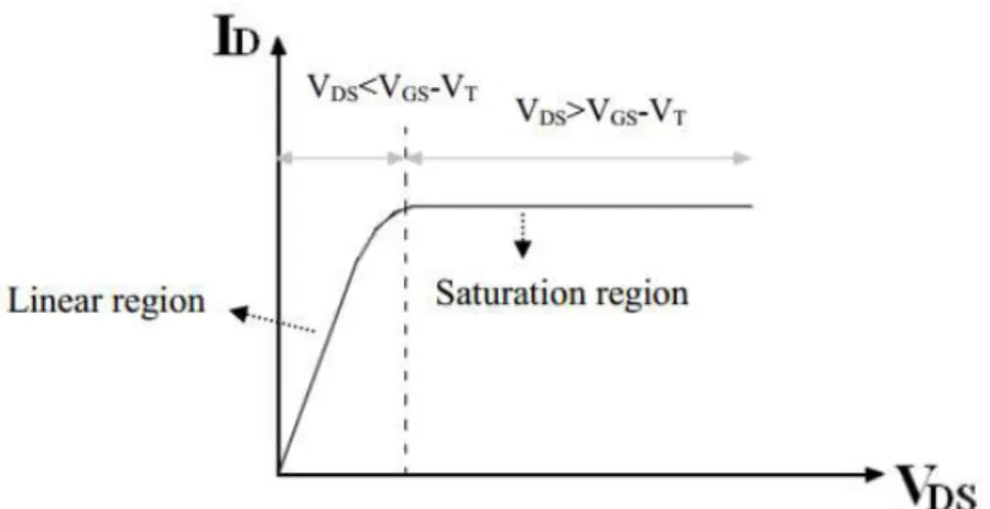
TFTs acts as traditional MOSFETs. Their main parameters are the voltage applied to the drain, the voltage applied to the gate and the drain current gener-ated by these two.
The drain voltage, VD, is normally a static value, but has to be high enough
in order to guarantee that the transistor will be turned ‘on’ when a certain value
of gate voltage is applied, whereas the source is connected to a lower voltage source. When VD is fixed, which value depends on the technology used, e.g., 1.2
V for traditional CMOS, or 10 V for IGZO TFTs, the behavior of the transistor stays entirely dependent of the gate voltage applied, VG. If VG doesn’t exceed the
threshold voltage VTh, it is considered to be in cutoff mode or weak-inversion
region; if VG continues to be slightly increased, current ID starts to flow and it is
assumed to be in triode mode or in its linear region, assuming VGS>Vth and
VDS<(VGS–Vth). This mode of operation can be useful on many operations, since
the transistor behaves as a variable resistor; if VG exceeds VTh and VDS ≥ (VGS–
Vth) it is ‘on’, also known as active or in saturation region. The current has its
10
Figure 2.3: Current-Voltage characteristic of a generic transistor.
2.4.
Electrical Parameter Extraction
In order to understand and design a circuit using IGZO TFTs, especially one that intents to be temperature invariant, it is crucial to extract some major electri-cal parameters. In this subchapter some methods describe how to electri-calculate the threshold voltage, the electron’s mobility, the capacitance per unit area and how they are related to the current-voltage characteristic.
2.4.1. Threshold Voltage
The threshold voltage is the parameter that dictates the state of the transis-tor, as being the minimum voltage applied to the gate that forms a conducting path between the source and drain terminals (electrons travel backwards in rela-tion to current’s convention way).
The Linear Extrapolation Method in the Linear Region is the most known and simplest method to extract VTh. It begins to powering the drain terminal to a
11
increments, e.g., 1 V or less, depending on the technology, and trace the respec-tive VGS-IDS characteristic. When VGS is high enough, electrons start to flow
through the conducting path and ID starts to grow exponentially until a
satura-tion region is reached, where the increase of VGS no longer affects the drain to
source current value.
Once the I-V characteristic is obtained, the threshold voltage is found at the intercept of the tangent in the inflexion point with the VGS axis, as in figure 2.4.
The inflexion point is given by the maximum of the transconductance of the tran-sistor [7].
Figure 2.4: VTh extraction, using Linear Extrapolation Method. Note: VTh is expressed as VT [7].
The expression of the drain curve in the linear region can be written as fol-lows:
𝐼𝐷 =𝑊𝐿 µ𝐶𝑜𝑥[𝑉𝐷𝑆(𝑉𝐺𝑆− 𝑉𝑇ℎ) −𝑉𝐷𝑆 2
2 ] (𝐴) (2.1)
Where W and L are the transistor’s width and length, respectively, µ is the
12
2.4.2. Charge Carrier Mobility
Charge carrier mobility defines how fast an electron can move in the semi-conductor channel when pulled by an electric field. In the particular case of TFTs, this can be called electron mobility and it is the parameter that outrages a-Si tech-nologies, which have 20 to 50 less carrier mobility.
Its extraction is calculated by plotting the square root of drain current as a function of the gate voltage. The value of µ is the result of the slope of the respec-tive curve, µSAT [3][8].
µ = µ𝑆𝑎𝑡 = 𝑚𝑆𝑎𝑡2 .𝑊. 𝐶2. 𝐿
𝑂𝑋 (
𝑐𝑚2
𝑉. 𝑠 ) (2.2)
Another method used for calculating the electron mobility is from the slope of the linear region of the drain current, µLin, against VGS curve, when a small drain to source bias VDS is applied [3].
µ = µ𝐿𝑖𝑛 = 𝑚𝐿𝑖𝑛.𝑊. 𝐶𝐿
𝑂𝑋 (
𝑐𝑚2
𝑉. 𝑠 ) (2.3)
However, mobility may be influenced by several factors, such as energy, interface charge density, process conditions, dielectric material selection, and others [3][9][10].
2.4.3. Capacitance per unit area
There are two main methodologies to extract the capacitance per unit area, or Cox. One of them just uses equation (2.4), which needs to know, in advance, the
exact values of the relative permittivity and of the oxide thickness, εr and τox,
re-spectively. εr is a specific value for each material, e.g., 3.9 for silicon oxide as
die-lectric layer [11] and 14 for Ta2O5 or a multilayer dielectric, both used in this
work.
𝐶𝑜𝑥 =𝜏𝜀𝑜𝑥 𝑜𝑥 =
𝜀0. 𝜀𝑟
𝜏𝑜𝑥 (
𝐹
𝑐𝑚2) (2.4)
13
Assuming the transistor is active, or in saturation region, Coxcan be
calcu-lated also by the slope of the accumulation charge density as a function of the applied gate voltage, or Q-V characteristic [12]. Figure 2.5 shows the charge den-sity as a function of the applied gate voltage.
Figure 2.5: Accumulation charge density as a function of the applied gate voltage [12].
VFB, or flat-band voltage, is the voltage at which there is no charge on the
15
3.
Low-Voltage Reference Topologies
3.1.
Introduction
In order to achieve the proposed objective of designing a voltage reference, it is necessary to understand its basics and what it is for. In third chapter a very widely used voltage reference named Bandgap Voltage Reference, or BGR, is pre-sented, which is a robust temperature independent voltage reference circuit that produces a fixed and constant voltage regardless of power supply variations, temperature changes and circuit loading from a device. Several topologies are shown and explained on the following subchapters, including the basic BGR used on low-voltage circuits, a low-voltage CMOS BGR based on partial com-pensation of MOSFET threshold voltage and mobility using current subtraction, which serves as base for this work, and a BGR with all TFT devices on glass sub-strate.
3.2.
Bandgap Reference Circuit
The basic principle of all temperature-independent bandgap voltage refer-ences is to sum two different internal voltage sources which one is proportional to the absolute temperature, or PTAT, and the other is complementary to the
16
solute temperature, or CTAT. By summing the two together, the temperature de-pendence can be cancelled. Graphical generic representations of a PTAT and CTAT characteristics are presented in figures 3.1. a) and 3.1. b), respectively.
In a theoretical way, if two voltage sources are, one PTAT and other CTAT, it means that one has a negative slope over temperature, meaning that the value of the characteristic being measured is dropping over temperature, and the other is the exact opposite. As the absolute value of the slopes is different, it is neces-sary to have some degree of manipulation of, at least, one of them, in order to cancel the temperature dependence. E.g., some topologies use transistors with different sizes and others use different resistor values.
Generically, a simple voltage reference bandgap circuit has to satisfy the following equations:
𝑉𝑅𝐸𝐹 = 𝑐1𝑉1+ 𝑐2𝑉2 (3.1)
𝜕𝑉𝑅𝐸𝐹
𝜕𝑇 = 𝑐1 𝜕𝑉1
𝜕𝑇 + 𝑐2 𝜕𝑉2
𝜕𝑇 = 0, (3.2)
where V1 and V2 are either CTAT and PTAT voltages, and c1 and c2 are values
that have to be dimensioned to accomplish Eq. (3.2). The referred equation is said to be null to accomplish temperature independence; it sums the slope of the PTAT voltage with the CTAT voltage and c1 and c2 are constants, such as the
width of the transistors, to compensate the overall dependence. b) a)
17
𝐼𝑓 𝑐1, 𝑐2 > 0, {
𝜕𝑉1
𝜕𝑇 < 0: 𝑁𝑒𝑔𝑎𝑡𝑖𝑣𝑒 𝑇𝑒𝑚𝑝𝑒𝑟𝑎𝑡𝑢𝑟𝑒 𝐶𝑜𝑒𝑓𝑓𝑖𝑐𝑖𝑒𝑛𝑡 (𝐶𝑇𝐴𝑇) 𝜕𝑉2
𝜕𝑇 > 0: 𝑃𝑜𝑠𝑖𝑡𝑖𝑣𝑒 𝑇𝑒𝑚𝑝𝑒𝑟𝑎𝑡𝑢𝑟𝑒 𝐶𝑜𝑒𝑓𝑓𝑖𝑐𝑖𝑒𝑛𝑡 (𝑃𝑇𝐴𝑇)
It has to be considered that, since this is a very basic bandgap reference in-troduction, only the linear effects of temperature dependence are taken in con-sideration.
A couple of examples are presented below using bipolar junction transis-tors, or BJT, since they are very simple and have interesting characteristics over temperature in this kind of applications.
Figure 3.2 shows a very simple bandgap circuit, where the supply voltage generates a current I1, that flows over the transistor T1. As T1 is in diode
configu-ration, I1 flows through its base forcing it to be in the active region and producing
a base-emitter voltage VBE, which is one of the inputs of the adder. A BJT, as any
other p-n junction device, exhibits a CTAT base-emitter voltage. On the other hand, the thermal voltage of the transistor, VT (=kT/q), is PTAT, thus it can be
connected to the other input of the adder.
Figure 3.2: Simple BGR circuit.
The output voltage of the circuit is then shown in Eq. (3.3):
𝑉𝑅𝐸𝐹 = 𝑉𝐵𝐸+ 𝑘𝑉𝑇. (3.3)
18
to the absolute temperature where VBE1 and VBE2 have opposite temperature
co-efficients and where the supply voltage VCC is converted to currents I1 and I2 that
are then mirrored to the output branch [13].
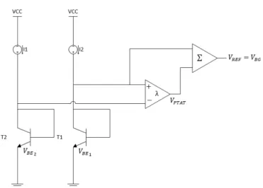
Figure 3.3: Simple BGR circuit, with two NPN transistors in diode-configuration with dif-ferent widths.
The output voltage equation of the example described above is:
𝑉𝑅𝐸𝐹= 𝑉𝐵𝐸1+ 𝜆(𝑉𝐵𝐸1− 𝑉𝐵𝐸2), (3.4)
where λ is the scale factor, VBE1 is the base-emitter voltage of the larger transistor
and VBE2 is the base-emitter voltage of the second transistor [13].
3.3.
A Low-Voltage CMOS Voltage Reference Based On Partial
Com-pensation of MOSFET Threshold Voltage and Mobility Using Current
Subtrac-tion
The method to generate a temperature-independent voltage reference de-scribed in chapter 3.3. serves as base for the development of the present work. Therefore, it is imperative to understand the working principles of the circuits reported by Dong and Allen [14], and Toledo, Dualibe and Canali [1], in order to be able to port and adapt them from CMOS to TFT technology.
19
Figure 3.4: CMOS bias circuit reported by [14].
The first characteristic to be noticed however, is that it is a low power cir-cuit, since the minimum possible supply voltage VDD has to be VT+2VDSAT. It
gen-erates a supply independent threshold-referenced bias voltage, VB, relative to the
ground. The dotted transistor N3 shows how the bias voltage VBis used to
gen-erate a supply-independent bias current IB[14].
Transistors P2 and P3 are PMOS and form a current mirror, as well as P1. Therefore, the currents on each of the three branches can be adjusted by choosing different transistor sizes, such as increasing or decreasing W, or width of each transistor, assuming a fixed L, or length; e.g. if P1 is considered to have a refer-ence drain-current and if it forms a current-mirror with P3, the current that flows on P3 is adjusted by its parameter W. Assuming that P1 and P3 are ideal transis-tors, adjusting the ratio of W of the two, multiples of the reference current can be generated.
𝐼𝑃3 = 𝐼𝑃1
(𝑊𝐿 )
𝑃3
(𝑊𝐿 )
𝑃1
, (3.5)
where IP1 and IP3 are the drain-currents across P1 and P3, respectively.
20
constant. Equations (3.6) and (3.7) show the bias voltage VB, and the resistor
cur-rent, IR, respectively [14]:
𝑉𝐵= 𝑉𝑇+ 𝑉𝐷𝑆𝑎𝑡𝑁1 (3.6)
𝐼𝑅 =𝑉𝑇+ 𝑉𝑅𝐷𝑆𝑎𝑡𝑁1 (3.7)
However, N2, P3 and P2 form a positive feedback path, but for stability purposes, the resulting feedback of the entire circuit, including N1, N2, P3, P2 and P1 should be negative, just as justified above; e.g. P1 and P2 form a current-mirror, so if the drain-current increases in P1, it will increase in P2:
𝐼𝑃2=
(𝑊𝐿 )
𝑃2
(𝑊𝐿 )
𝑃1
. 𝐼𝑃1 (3.8)
𝛥𝐼𝑃2=
(𝑊𝐿 )
𝑃2
(𝑊𝐿 )
𝑃1
. 𝛥𝐼𝑃1 (3.9)
Thus, the drain-current of the transistor N1 will have the same behavior of P2 and its variation has a small-sign relation of:
𝛥𝐼𝑁1 = 𝛥𝐼𝑃1. 𝑅. 𝑔𝑚𝑁1 , (3.10)
where gmN1is the transconductance of the transistor N1, and:
𝑅 =𝑉𝑇+ 𝑉𝐼𝐷𝑆𝑎𝑡𝑁1
𝑃1 (3.11)
𝑔𝑚𝑁1 =𝑉2𝐼𝑁1
𝐷𝑆𝑎𝑡𝑁1=
2𝐼𝑃2
𝑉𝐷𝑆𝑎𝑡𝑁1=
2(𝑊𝐿 )𝑃2
(𝑊𝐿 )
𝑃1
. 𝐼𝑃1
𝑉𝐷𝑆𝑎𝑡𝑁1 .
21 Equation (3.10) is now:
𝛥𝐼𝑁1= 2
(𝑊𝐿 )
𝑃2
(𝑊𝐿 )
𝑃1
. 𝛥𝐼𝑃1. (1 +𝑉 𝑉𝑇 𝐷𝑆𝑎𝑡𝑁1)
= 2. 𝛥𝐼𝑃2. (1 +𝑉 𝑉𝑇 𝐷𝑆𝑎𝑡𝑁1)
> 𝛥𝐼𝑃2 ,
(3.13)
which means that the drain voltage of N1 and the gate voltage of N2 will de-crease, then the currents of N2, P3, P2 and P1 will decrease. Therefore, the result-ing feedback of N1, N2, P3, P2 and P1 is negative [14].
The effect of the supply-voltage variations is the same as that of the current variations of P1 and P2. Supposing that VDD increases, if the gate-to-source
volt-ages of N1 and N2 keep constant, the drain-to-source voltvolt-ages of P1, P2 and N2 will increase, and then the drain currents of N2, P3 and P1 will increase. On the other hand, if the gate-to-source voltages of N1 and N2 increase, the drain cur-rents of N1, N2, P3 and P1 will also increase. The same analysis as for the drain-current increase of P1 and P2, which is illustrated above, from equation (3.8) to equation (3.13), can be used to show that the current will remain constant [14].
Nevertheless, the circuit reported by [14] still suffers from inadequate sen-sibility to temperature variations and cannot be used as such, i.e. as an accurate voltage reference [1][15]. Therefore, a new architecture is proposed [1], based on BGR method, as seen in figure 3.5.
22
Figure 3.5: Currents subtraction scheme, reported by [1].
By direct inspection, using Kirchhoff's Current Law, or KCL, which states that the sum of all the input and output currents is equal to zero, the equation that dictates VREF is calculated as follows, using the node between ICTAT1 and
ICTAT2:
𝐼𝐶𝑇𝐴𝑇1 = 𝐼𝐶𝑇𝐴𝑇2+𝑉𝑅𝑅𝐸𝐹 3
⇔ 𝑉𝑅𝐸𝐹 = (𝐼𝐶𝑇𝐴𝑇1− 𝐼𝐶𝑇𝐴𝑇2)𝑅3
⇔ 𝑉𝑅𝐸𝐹 = (𝑉𝐶𝑇𝐴𝑇1𝑅
1 − 𝐾
𝑉𝐶𝑇𝐴𝑇2
𝑅2 ) 𝑅3
⇔ 𝑉𝑅𝐸𝐹 = 𝑅𝑅3
1(𝑉𝐶𝑇𝐴𝑇1− 𝐾
𝑅1
𝑅2𝑉𝐶𝑇𝐴𝑇2) (3.14)
Thus, the value of VREF is entirely dependent on the ratios between R3 and
R1, and R1 and R2. A value of K has to be considered, because the output voltage
of the overall circuit, VREF, present in figure 3.6 as VO, is the voltage-drop across
transistor T7, which is, in turn, connected to T8, which makes part of a
current-mirror generator. The expression of K is then:
𝐾 = (𝑊𝐿 )7 (𝑊𝐿 )
8
23
Figure 3.6: Proposed voltage reference reported by [1].
Note that the I1 and I2 current generators are the circuits explained in the
beginning of this chapter.
The next step, after understanding how the resistors R1, R2 and R3 influence
the output voltage, is to guarantee that this value doesn’t change with tempera-ture. Thus, the partial derivative of VREF in temperature should be zero.
𝜕𝑉𝑅𝐸𝐹
𝜕𝑇 = 𝑅3
𝑅1(
𝜕𝑉𝐶𝑇𝐴𝑇1
𝜕𝑇 − 𝐾 𝑅1
𝑅2
𝜕𝑉𝐶𝑇𝐴𝑇2
𝜕𝑇 ) = 0 (3.16)
It has to be noticed too that R1, R2 and R3 are not considered to be ideal
resistors but, as they are fractions, and the temperature dependences between R3
and R1, and R1 and R2, are fractions too, they cancel out. To verify the condition
of equation (3.16), the absolute value in brackets must be zero, which gives the following relation between R1 and R2:
𝜕𝑉𝐶𝑇𝐴𝑇1
𝜕𝑇 − 𝐾 𝑅1
𝑅2
𝜕𝑉𝐶𝑇𝐴𝑇2
𝜕𝑇 = 0
⇔
𝜕𝑉𝐶𝑇𝐴𝑇1
𝜕𝑇 𝜕𝑉𝐶𝑇𝐴𝑇2
𝜕𝑇
= 𝐾𝑅𝑅1
2 (3.17)
It can be concluded that the ratio between R1 and R2 should be as such as it
cancels the TC differences between VCTAT1 and VCTAT2, whereas the ratio between
R3 and R1 sets the reference voltage to a desired level. Since both relations share
24
that correlates the three and achieves the optimum balance, from a thermal point of view.
Attending to the proposed voltage reference circuit, as it uses a current sub-traction scheme, currents I1 and I2 are modulated according to R1 and R2 values.
They can be seen as potentiometers. Each one of I1 and I2 current generators have
two different currents, with different magnitude and temperature coefficients. One current is subtracted from the other with a proper scale factor and the re-sulting current goes through a resistor in order to provide a voltage reference with an almost null TC [1].
All NMOS and PMOS transistors of the proposed circuit operate in strong inversion, thus I1 and I2 currents can be obtained through the current expressions
of T3 and T10, respectively. In order to simplicity this explanation, only I1
expres-sions is present below, since I2 is generated by the exact same circuit.
𝐼1 = 12 𝜇𝑛𝐶𝑂𝑋(𝑊𝐿 )
1(𝑉𝐺𝑆− 𝑉𝑇ℎ𝑁) 2
⟺ (𝑉𝐺𝑆− 𝑉𝑇ℎ𝑁)2 = 2𝐼1
𝜇𝑛𝐶𝑂𝑋(𝑊𝐿 )1
⟺ 𝑉𝐺𝑆− 𝑉𝑇ℎ𝑁 = √ 2𝐼1
𝜇𝑛𝐶𝑂𝑋(𝑊𝐿 )1
, 𝑉𝐺𝑆 = 𝑅1𝐼1
⟺ 𝑅1𝐼1− √ 2𝐼1
𝜇𝑛𝐶𝑂𝑋(𝑊𝐿 )1
− 𝑉𝑇ℎ𝑁= 0
⟺ 𝐼1 =𝑉𝑅𝑇ℎ𝑁
1 +
1 + √1 + 2𝑅1. 𝑉𝑇ℎ𝑁. 𝜇𝑛𝐶𝑂𝑋. (𝑊𝐿 )1
𝜇𝑛𝐶𝑂𝑋. (𝑊𝐿 )1. 𝑅12
(3.18)
Equation (3.18) demonstrates that I1, and so I2, depend on the values of R1,
and so R2, respectively, as well as the ratios (W/L)1 and (W/L)2. However, from
Ohm’s law, I1 is the quotient between VCTAT1 and R1, so VCTAT1 is:
𝑉𝐶𝑇𝐴𝑇1 = 𝑉𝑇ℎ𝑁+
1 + √1 + 2𝑅1. 𝑉𝑇ℎ𝑁. 𝜇𝑛𝐶𝑂𝑋. (𝑊𝐿 )1
𝜇𝑛𝐶𝑂𝑋. (𝑊𝐿 )1. 𝑅1
25
Since the objective of this method is to cancel the TC using current subtrac-tion, equation (3.19) must be differentiated in temperature. It will then give the variation of the output voltage of I1 current generator, as well as the variation of
the output voltage of the I2 current generator. Both equations are, respectively,
equations (3.20) and (3.21).
𝜕𝑉𝐶𝑇𝐴𝑇1
𝜕𝑇 = 𝑉𝑇ℎ𝑁
( 1 𝑉𝑇ℎ𝑁 𝜕𝑉𝑇ℎ𝑁 𝜕𝑇 + 1
𝑉𝑇ℎ𝑁𝜕𝑉𝜕𝑇 +𝑇ℎ𝑁 𝑅11
𝜕𝑅1
𝜕𝑇 +𝜇1𝑁
𝜕𝜇𝑁
𝜕𝑇
√1 + 2𝑅1. 𝑉𝑇ℎ𝑁. 𝜇𝑛𝐶𝑂𝑋. (𝑊𝐿 )1
)
+1 + √1 + 2𝑅1. 𝑉𝑇ℎ𝑁. 𝜇𝑛𝐶𝑂𝑋. (𝑊𝐿 )1 𝜇𝑛𝐶𝑂𝑋. (𝑊𝐿 )1. 𝑅1
(−𝜇1
𝑁 𝜕𝜇𝑁 𝜕𝑇 − 1 𝑅1 𝜕𝑅1 𝜕𝑇 ) (3.20)
𝜕𝑉𝐶𝑇𝐴𝑇2𝜕𝑇 = 𝑉𝑇ℎ𝑃
( 1 𝑉𝑇ℎ𝑃 𝜕𝑉𝑇ℎ𝑃 𝜕𝑇 + 1
𝑉𝑇ℎ𝑃𝜕𝑉𝜕𝑇 +𝑇ℎ𝑃 𝑅12
𝜕𝑅2
𝜕𝑇 +𝜇1𝑃
𝜕𝜇𝑃
𝜕𝑇 √1 + 2𝑅2. 𝑉𝑇ℎ𝑃. 𝜇𝑃𝐶𝑂𝑋. (𝑊𝐿 )2
)
+1 + √1 + 2𝑅2. 𝑉𝑇ℎ𝑃. 𝜇𝑃𝐶𝑂𝑋. (𝑊𝐿 )2 𝜇𝑃𝐶𝑂𝑋. (𝑊𝐿 )2. 𝑅2
(−𝜇1
𝑃 𝜕𝜇𝑃 𝜕𝑇 − 1 𝑅2 𝜕𝑅2 𝜕𝑇 ) (3.21)
Two equations are needed, for two current generators. Equation (3.20) shows the behavior of one half of the entire circuit, whereas equation (3.21) the other half. It has to be noticed that equation (3.20) only uses the characteristics of the NMOS transistors, while equation (3.21) uses PMOS’s, given the fact that both currents I1 and I2 are mirrored into the transistors T6 and T7.
𝐼𝑇6 = 𝐼1
(𝑊𝐿)
6
(𝑊𝐿)
3
(3.22)
𝐼𝑇7 = 𝐼2
(𝑊𝐿)
7
(𝑊𝐿)
8
(3.23)
The key elements to develop this topology are, first of all, to understand how the CMOS bias circuit presented initially works, theoretically and by simu-lation; to choose two currents, I1 and I2, according to the technology used and
26
influences the output behavior of the overall circuit, since it is responsible for driving the most significant part of the output current.
3.4.
Design of a Bandgap Voltage Reference Circuit with all TFT
De-vices on Glass Substrate in a 3 µm LTPS Process
Since there is a lack of voltage reference topologies that use TFT devices, another design is introduced which can probably be implemented with IGZO TFTs, given the fact that they are both n-type transistors and both use 10 V power supplies, as well as the ones that can be used in glass applications.
As seen in subchapter 3.2., the conventional BGR uses Bipolar Junction Transistors, of BJTs, and other topologies use diodes instead, or BJTs connected in diode configurations [16], [17]. Knowing that these have negative temperature coefficients, or TCs, the main idea is to use the temperature-dependent voltage-drop across the diode-connected BJTs to modulate and stabilize the output volt-age, through a positive TC, generated by a proper circuit design. The incorpora-tion of BJTs into CMOS technology somehow makes the process control difficult. Therefore, it was also considered using only MOSFETs in the BGR circuit to sim-plify the process and to reduce the operating voltage/power. The voltage across MOSFETs is sensitive to temperature only when the MOSFETs are biased in the subthreshold region. The gate-to-source voltage of MOSFETs in sub-threshold region is strongly dependent on temperature and exhibits a negative temperature coefficient [18].
The conventional BGR circuit incorporated with BJTs or diodes is a great challenge for the LTPS process since the characteristics of the poly-Si BJTs or the poly-Si diodes are still unknown or lack reliable control. The use of LTPS TFT devices biased in the sub-threshold region is also not practical because the poly-Si TFT devices often suffer from significant threshold voltage variation. However, the I-V characteristics of LTPS TFT devices have been found to be strongly dependent on temperature when the devices are operated in the saturation region [18]–[20].
27
sum of a base-emitter voltage, VEB, of BJT Q3 and the voltage-drops across the
upper resistor R2. The BJTs, Q1, Q2, and Q3, are typically implemented by the
di-ode-connected parasitic vertical PNP bipolar junction transistors in the CMOS process with the current proportional to exp (VEB/VT), where VT (=kT/q) is the
thermal voltage. Under constant current bias, VEB is strongly dependent on VT, as
well as on temperature. The current mirror, formed by M1, M2, and M3, is
de-signed to bias Q1, Q2, and Q3 with identical current. Then, the voltage drop on
the resistor R1 can be expressed by equation (3.24) [18]:
𝑉𝑅1= 𝑉𝑇𝑙𝑛 (𝐴𝐴1
2) (3.24)
where A1 and A2 are the emitter areas of Q1 and Q2. It is noted that VR1 exhibits a
positive temperature coefficient when A1 is larger than A2. Besides, since the
cur-rent which flows through R1is equal to the current which flows through R2, the
output voltage of the traditional bandgap voltage reference circuit can be written as [18]:
𝑉𝑅𝐸𝐹 = 𝑉𝐸𝐵3+𝑅𝑅2
1𝑉𝑇𝑙𝑛 (
𝐴1
𝐴2) (3.25)
The second item in equation (3.25) is proportional to the absolute tempera-ture, PTAT, which is used to compensate the negative temperature coefficient of VEB3. In general, the PTAT voltage comes from the thermal voltage, which is quite
smaller than that of VEB. After multiplying the PTAT voltage with an appropriate
factor, R2/R1, and summing with VEB, the output voltage VREF of bandgap
28
Figure 3.7: The traditional bandgap voltage reference circuit realized in CMOS technol-ogy with parasitic vertical PNP bipolar junction transistors [18].
For LTPS TFT devices, the drain current IDS of devices operating in the
sat-uration region can be expressed as [21]:
𝐼𝐷𝑆 =2𝐿 µ𝑊 0𝐶𝑜𝑥(𝑉𝐺𝑆 − 𝑉𝑇𝐻)2𝑒(− 𝑉
𝐵
𝑉𝑇) (3.26)
where µ0 is the carrier mobility within the drain, L denotes the effective channel
length, W is the effective channel width, Cox is the gate oxide capacitance per unit
area, VTh is the threshold voltage of TFT device, and VGS is the gate-to-source
voltage of TFT device. VB is the potential barrier at grain boundaries which is
associated with the crystallization quality of the poly-Si film [18]. Under small VGS, VB is large. When the VGS increases, VB decreases rapidly. When the devices
are operated under small VGS, it is found that the drain current IDS of devices is
dominated by the exponential term and can be estimated by [18]:
𝐼𝐷𝑆 = 𝑊𝛼𝑒(− 𝑉
𝐵
𝑉𝑇) . (3.27)
Where α is treated as a constant under small gate bias VGS. Then, the
equa-tion for VB can be derived as [18]:
𝑉𝐵 = 𝑉𝑇𝑙𝑛 (𝑊𝛼𝐼𝐷𝑆) = (𝑘𝑇𝑞) 𝑙𝑛 (𝑊𝛼𝐼𝐷𝑆) . (3.28)
29
𝛥𝑉𝐵 =𝑘𝛥𝑇𝑇 ln (𝑊𝛼𝐼
𝐷𝑆). (3.29)
From equation (3.29), it can be found that the temperature coefficient (TC) of VB can be modulated by the channel width. The larger channel width gives
rise to the larger TC of VB[18].
The variation of VB is related to the variation of VGS. Assuming that the
variation of VGS, or ΔVGS, is very small, a negative linear approximation can be
given between ΔVB and ΔVGS as [18]:
𝛥𝑉𝐺𝑆 = −𝑚 𝛥𝑉1 𝐵= −𝑘𝛥𝑇𝑚𝑞 ln (𝑊𝛼𝐼 𝐷𝑆) = −
𝛥𝑉𝐵𝛥𝑇
𝑚𝛥𝑇 ,
(3.30)
where m is the absolute value of the slope under linear approximation.The de-vices biased at small VGS can exhibit a large VB if its channel width is enlarged
[18].
The channel width of M6, or W6, is larger than the channel width of M7, or
W7, so the TC of M6 is more negative than the TC of M7. The voltage-drop across
the resistor R1, VR1, therefore exhibits a positive TC. If the dependence of m on
VGS is neglected, the variation of VR1,ΔVR1, as a function of ΔT can be expressed
as [18]:
𝛥𝑉𝑅1= 𝑘𝛥𝑇𝑚𝑞 ln (𝑊𝑊6 7) =
𝑘𝛥𝑇 𝑚𝑞 𝑙𝑛 𝑁.
30
Figure 3.8: The implementation of the new proposed bandgap voltage reference circuit with all TFT devices in a LTPS process [18].
Obviously, ΔVR1 is proportional to the absolute temperature, or simply
PTAT. Hence, a PTAT loop is formed by M6, M7, and R1. The PTAT current
vari-ation ΔI1 can be written as [18]:
𝛥𝐼1 = 𝑚𝑞𝑅𝑘𝛥𝑇 1ln 𝑁,
(3.32)
where N (=W6/W7) is the channel width ratio of M6 and M7, and VT is the thermal
voltage. The current mirror, which is composed of M1, M2, and M3, imposes equal
currents in these three branches I1, I2, and I3 of the circuit. The output voltage,
VREF, is the sum of a gate-source voltage of TFT M8, VGS8, and the voltage-drop
across the upper resistor VR2. Therefore, the output voltage variation, ΔVREF, of
the new proposed bandgap reference circuit can be expressed as [18]:
𝛥𝑉𝑅𝐸𝐹 = 𝛥𝐼3𝑅2+ 𝛥𝑉𝐺𝑆8=𝑅𝑅21𝑘𝛥𝑇𝑚𝑞ln 𝑁 + 𝛥𝑉𝐺𝑆8 , (3.33)
where R1 and R2 are the resistors shown in figure 3.8. The first item in equation
(3.33) with positive TC is proportional to the absolute temperature, PTAT, which is used to compensate the negative temperature coefficient of ΔVGS8. After
mul-tiplying the PTAT voltage with an appropriate factor, which is the proper ratio between the resistors, and summing with ΔVGS8, the output voltage of bandgap
31
3.5.
Conclusions
Various methodologies can be used to generate a voltage reference that is temperature independent. This chapter presented the basics of what is a bandgap voltage reference, as well as a more sophisticated methodology that can be used in thin film transistors. Another non-bandgap was introduced, in chapter 3.4., which will be implemented further.
This type of voltage reference circuits can be widely used and it is impera-tive that they are well dimensioned, since there are some specific circuits that are very voltage reference dependent, such as data conversion systems, ADCs and DACs. The referred examples always use comparators with the voltage reference signal as input. Any kind of error on VREF and it will compromise the output
33
4.
Design Methodology and Electrical
Simula-tions using a standard 130 nm Technology
4.1.
Introduction
Before starting the implementation and development of the project using, effectively TFTs, chapter 4 aims to explain how the process of generating a volt-age reference is done using the method described in subchapter 3.3., now in a practical analysis. The technology in use is a generic and well known standard 130 nm.
The first step that must be done is to verify if all the characteristics of the needed equations are known, and if not, they have to be extracted by simulation from the circuit or the components themselves. These procedures are carefully defined and illustrated on the respective subchapters. The second step is to re-place the unknown terms of the equations with the extracted or calculated values and observe the respective results; in the present case, it is done with a mathe-matical software tool, such as MathCAD, referred earlier, in chapter 1. At this stage, it is possible to have a first guess of values which corresponds to the order of magnitude of the resistors R1 and R2. The third and final step is to port the
obtained values from MathCAD to Cadence’s simulation tool and vary them un-til the primary objective is achieved, which is a compensated voltage reference with as minimal output voltage variation as possible.
34
4.2.
Mathematical Analysis
To calculate the order of magnitude of the three major variables, a mathe-matical study is realized. Considering that the technology in question is a stand-ard 130 nm, where some of the respective values are already known, the first step is to look to the needed equations and realize if there are any missing parameters. Before a further analysis, table 4.1 exhibits all the parameters previously known of the mentioned technology, for NMOS and PMOS transistors, respec-tively, while table 4.2 presents the respective width and length transistor sizes.
Table 4.1: Technology Parameters.
NMOS PMOS
VDD [V] 1.2
VDSat [mV] 100
|VTh| [V] 0.38 0.33
µ.Cox[µ𝐀
𝐕𝟐] 500 100
Table 4.2: Transistor Sizes.
NMOS PMOS
Width [µm] 10 10
Length [µm] 1 1
The value of VDD is the supply voltage for this technology and VDSAT is the
35
Observing equations (3.20) and (3.21), the differentials in temperature of VCTAT1 and VCTAT2 depend on non-ideal resistors, but since the main goal of this
work is to design the circuit and produce the PCB with external resistors, they are considered as ideal components. Therefore,
1 𝑅1
𝜕𝑅1
𝜕𝑇 = 0
(4.1)
1 𝑅2
𝜕𝑅2
𝜕𝑇 = 0
(4.2)
The following lines are about the extraction of the threshold voltage of the NMOS and NMOS transistors, as well as the electron mobility. To extract these parameters, the transistors have to operate, in most cases, in the saturation re-gion, so a gate voltage of 1 V is applied and the circuit is shown in figure 4.1.
Figure 4.1: Circuit to extract the needed parameters of a NMOS transistor.
36
Figure 4.2: Simulation of VTh over temperature of the NMOS transistor.
Figure 4.3: Simulation of VTh over temperature of the PMOS transistor.
As both graphs are almost perfectly linear, a simple first order derivative can be made using two arbitrary points; see equation (4.3). The results are pre-sented on table 4.3.
𝜕𝑉𝑇ℎ
𝜕𝑇 = 𝛥𝑉𝑇ℎ
𝛥𝑇 =
𝑉𝑇ℎ(𝑇2) − 𝑉𝑇ℎ(𝑇1)
37
Table 4.3: Threshold voltage variation over temperature of NMOS and PMOS transistors of a 130 nm technology.
NMOS PMOS
𝝏𝑽𝑻𝒉
𝝏𝑻 [ 𝐦𝐕
𝐊] -0.8 0.91(6)
The last step to be able to complete the missing terms of equations (3.20) and (3.21) is to find the respective variations of the electron’s mobility, in order to temperature.
It is not possible to simulate the electron’s mobility by software, so a work-around solution has to be found using the conduction parameter. From equation (3.18):
𝐾𝑁,𝑃 =𝑊. (𝑉2𝐼𝐷. 𝐿
𝐺𝑆 − 𝑉𝑇)2 (4.4)
The simulations for NMOS and PMOS transistors are represented in fig-ures 4.4 and 4.5, respectively.
38
Figure 4.5: Simulation of KP over temperature of the PMOS transistor.
Linear characteristics can be observed, therefore the same method used to calculate the threshold voltage, equation (4.3), can be applied once again. Table 4.4 shows the slopes of the graphs of figures 4.4 and 4.5 using a first order deriv-ative.
Table 4.4: Conduction parameter variation over temperature of NMOS and PMOS tran-sistors of a standard 130 nm technology.
NMOS PMOS
𝝏𝒎𝑲
𝝏𝑻 [ µ𝐀 𝐕𝟐
𝐊
⁄ ] -0.594611 0.03917(7)
It is also known that:
𝐾𝑁,𝑃 = µ𝑁,𝑃. 𝐶𝑜𝑥 (4.5)
So,
𝜕𝐾𝑁,𝑃
𝜕𝑇 = 𝜕µ𝑁,𝑃
𝜕𝑇 . 𝐶𝑜𝑥
⟺𝜕µ𝜕𝑇 =𝑁,𝑃 𝜕𝐾𝑁,𝑃
𝜕𝑇 𝐶𝑜𝑥
39
Assuming that the values of the capacitance per unit areaare constant, then the final unknown values can now be calculated in order to demystify equations (3.20) and (3.21).
𝐶𝑜𝑥 =𝜀𝑡𝑜𝑥 𝑜𝑥 =
𝜀0. 𝜀𝑟
𝑡𝑜𝑥
(4.7)
The first value of the numerator of equation (4.7), ε0, is the vacuum
permit-tivity, which value is 8.854x10⁻¹⁴ F/cm, whereas εr is the relative permittivity. For
this technology εr is 3.9.
Knowing that the software simulation tool returns values that are relatively close to real, the value of tox can be extracted from its libraries. The purpose of
this is to acquire first guess values which are as trustworthy as possible. Table 4.5 shows the values of tox for each type of transistor.
Table 4.5: Thickness oxide parameters of NMOS and PMOS transistors of a 130 nm tech-nology.
NMOS PMOS
𝒕𝒐𝒙 [𝐧𝐦] 2.73 2.86
Equation (4.7) can now be calculated and then the effective values of the
variation of the electron’s electrical mobility over temperature can be extracted mathematically. Their values are shown on the following tables, 4.6 and 4.7, re-spectively.
Table 4.6: Capacitance per unit area of NMOS and PMOS transistors of a standard 130 nm technology.
NMOS PMOS
40
Table 4.7: Electron’s mobility over temperature of NMOS and PMOS transistors of a standard 130 nm technology.
NMOS PMOS
𝝏µ 𝝏𝑻 [
𝐜𝐦𝟐
𝐕. 𝐬. 𝐊] -0.47 0.032
At this point, it is possible to draw and analyze the two graphs that corre-spond to the behavior of VCTAT1 and VCTAT2. According to the principle of the
bandgap voltage reference, one graph should be PTAT, while the other CTAT, with different TCs. In figures 4.6 and 4.7 are plotted the equations (3.20) and (3.21), respectively, with different size relations, from 10 to 100.
Figure 4.6: Temperature characteristics of VCTAT1, from 273 K to 373 K. The black line
rep-resents the size relation (W/L) = (10 µm/1 µm).
𝜕𝑉𝐶𝑇𝐴𝑇1
𝜕𝑇 = −0,89 𝑚𝑉
41
Figure 4.7: Temperature characteristics of VCTAT2, from 273 K to 373 K. The black line
rep-resents the size relation (W/L) = (10 µm/1 µm).
The voltage across the resistor R1 starts in -243 mV, at 273 ºK, and decreases
all the way to -332 mV, at 373 ºK, which is a variation of -0.89 mV/K; whereas the voltage across the resistor R2 starts in 266 mV, at 273 ºK, and increases until
364 mV, at 373 ºK, which is a variation of 0.976 mV/K. The calculated slopes are in the same magnitude of values and are very close to each other. VCTAT1 and
VCTAT2 are CTAT and PTAT, respectively, and their values are in the range of
what is expected for this technology. Thus, this is the confirmation that all the previous calculations are correct and the first guess for the resistors can also be accomplished. Although, the values of VCTAT1 and VCTAT2may differ when
com-pared to the simulation results, since the simulation has several parameters, which are intrinsic to the technology, and are not considered in this analysis. However, it does not affect the final purpose of this step.
Since VCTAT1 and VCTAT2 are now known, theoretically it would be possible
to cancel the TC of the circuit from equation (3.17):
−0.89 𝑚𝑉𝐾 0.976 𝑚𝑉𝐾 = 𝐾
𝑅1
𝑅2
⟺ 𝐾𝑅𝑅1
2 = −0.91 (4.8)
Although, analyzing carefully article [1], the values of its resistors R1 and R2
are chosen according to the predefined currents I1 and I2, which are 10 µA and 1
𝜕𝑉𝐶𝑇𝐴𝑇2
𝜕𝑇 = 0,976 𝑚𝑉
42
µA, respectively. From Ohm’s law, R1 and R2are then 40 kΩ and 400 kΩ,
respec-tively.
Using the same methodology and given that the present technology is sim-ilar to the technology used by [1], from equation (3.18) the values from the resis-tors used in this work are, coincidentally, the same. By successive mathematical simulations from (3.18) to achieve currents near to the referred numbers, the val-ues of the resistors R1 and R2 are:
𝑅1 = 40 𝑘Ω
𝑅2 = 400 𝑘Ω
Which result in currents with values of:
𝐼1 = 11.171 µ𝐴
𝐼2 = 0.933 µ𝐴
The overall conclusions that can be taken from the theoretical and mathe-matical analysis are, essentially, that the resistors R1 and R2 vary in different
scales, being R2 around ten times greater than R1. Nevertheless, more important
than this is that the first resistor has a range of values that goes in tens of thou-sands and the second in hundreds of thouthou-sands of Ohms. Therefore, the values which each of the resistors will have on the next step of the project are now well known. Relative to resistor R3, it is not taken in consideration because, from
equa-tions (3.14) and (3.16) it can be seen that it has no effect on canceling the TC of the circuit. Its only objective is to set the output voltage to a desired level. For this technology and considering all the previously presented values, if equation (3.14) is solved with an input range of R3 varying from 50 kΩ to 100 kΩ, the output
voltage results are, respectively, 0.605 V and 1.21 V. Then, theoretically, this volt-age reference circuit should be able to feed effectively any low-voltvolt-age circuit downstream using, e.g., the same technology.
43
4.3.
Simulation Results
This subchapter presents the results of the simulations from the previous analysis. Before the final circuit, namely figure 3.6, I1 and I2 current generators
are isolated from each other in order to verify if the respective currents and volt-ages behaviors are in conformity with the previous results.
Figure 4.8: I1 current generator.
From the previous analysis, VCTAT1 should be CTAT. However, the
simula-tion shows that VCTAT1 has the opposite behavior, being PTAT. The main reason
for this to happen should have to do with some signal change on equation (3.20). As this bandgap voltage reference is based on current subtraction, the essential is that both I1 and I2 are CTAT, so if one increases or decreases, the other does the
same in a way that the respective subtraction cancels the TC. Figures 4.9 and 4.10 show the respective simulation results for VCTAT1 and I1 for different resistor

![Figure 2.4: V Th extraction, using Linear Extrapolation Method. Note: V Th is expressed as V T [7]](https://thumb-eu.123doks.com/thumbv2/123dok_br/16575891.738277/31.892.271.673.453.717/figure-extraction-using-linear-extrapolation-method-note-expressed.webp)
![Figure 2.5: Accumulation charge density as a function of the applied gate voltage [12]](https://thumb-eu.123doks.com/thumbv2/123dok_br/16575891.738277/33.892.341.641.259.502/figure-accumulation-charge-density-function-applied-gate-voltage.webp)
![Figure 3.6: Proposed voltage reference reported by [1].](https://thumb-eu.123doks.com/thumbv2/123dok_br/16575891.738277/43.892.166.772.128.358/figure-proposed-voltage-reference-reported.webp)
![Figure 3.7: The traditional bandgap voltage reference circuit realized in CMOS technol- technol-ogy with parasitic vertical PNP bipolar junction transistors [18]](https://thumb-eu.123doks.com/thumbv2/123dok_br/16575891.738277/48.892.352.540.126.387/figure-traditional-reference-realized-parasitic-vertical-junction-transistors.webp)
![Figure 3.8: The implementation of the new proposed bandgap voltage reference circuit with all TFT devices in a LTPS process [18]](https://thumb-eu.123doks.com/thumbv2/123dok_br/16575891.738277/50.892.346.565.127.398/figure-implementation-proposed-bandgap-voltage-reference-circuit-devices.webp)

