Carlos Daniel Gonçalves Marques
Bachelor in Micro and Nanotechnologies EngineeringDevelopment of high-resolution shadow masks
using thin membranes of parylene-C for
patterning microelectronic devices
Dissertation submitted in partial fulfillment of the requirements for the degree of
Master of Science in
Micro and Nanotechnologies Engineering
Adviser: Prof. Dr. Joana Maria Dória Vaz Pinto Morais Sarmento, Invited Assistant Professor, NOVA University of Lisbon
Examination Committee
Chair: Prof. Dr. Rodrigo Ferrão de Paiva Martins Rapporteurs: Prof. Dr. Luís Miguel Nunes Pereira
Prof. Dr. Joana Maria Dória Vaz Pinto Morais Sarmento
Development of high-resolution shadow masks using thin membranes of parylene-C for patterning microelectronic devices
Copyright © Carlos Daniel Gonçalves Marques, Faculty of Sciences and Technology, NOVA University Lisbon.
The Faculty of Sciences and Technology and the NOVA University Lisbon have the right, perpetual and without geographical boundaries, to file and publish this dissertation through printed copies reproduced on paper or on digital form, or by any other means known or that may be invented, and to disseminate through scientific repositories and admit its copying and distribution for non-commercial, educational or research purposes, as long as credit is given to the author and editor.
This document was created using the (pdf)LATEX processor, based on the “novathesis” template[1], developed at the Dep. Informática of FCT-NOVA [2].
"Try and leave this world a little better than you found it" Baden-Powell’s Last Message, Robert Baden-Powell
Ac k n o w l e d g e m e n t s
Primeiramente um agradecimento à Faculdade de Ciências e Tecnologia da Universidade Nova de Lisboa, por me proporcionar excelentes momentos e condições para completar esta etapa.
Um agradecimento à professora Elvira Fortunato e ao professor Rodrigo Martins por disponibilizarem o CENIMAT e o CEMOP e todos os seus equipamentos para que fosse possível realizar este trabalho.
Um grande obrigado à minha orientadora, Joana Vaz Pinto, pela ajuda e dedicação. Um obrigado a todos os professores e investigados, Rita Branquinho, Rui Igreja, Joana Neto, Emanuel Carlos, Ana Santa, Cátia Figueiredo, Inês Martins, Maria Pereira, Sara Silvestre, Carolina Marques, André Moura, Pedro Centeno, Sónia Pereira e Alexandra Gonçalves pela ajuda prestada durante este trabalho.
Um agradecimento a todos o que fizeram a tese ao mesmo tempo que eu, Federico Fonseca, Leonor Duarte, Paulo Fernandes, Renato Nora, Guilherme Ferreia, Guilherme Castelo, Mafalda Pina, Frederico Neves e Bernardo Caetano.
Um obrigado à minha família, mãe, pai, irmãos, madrinha e afilhados por tudo o que fazem por mim no dia a dia. Um obrigado à minha falecida avó Zita que tudo fez por mim enquanto pôde.
Aos meus colegas de curso e especialmente ao Pedro Moura, André Lourenço e Jorge Mafalda.
Um obrigado aos meus amigos, João Rangel, João Alves e Miguel Isabel e restante Alto do Índio FC.
A b s t r a c t
In order to fabricate microelectronic devices, patterning techniques such as photolithog-raphy or shadow mask patterning must be performed. This last technique uses a physical mask to block regions on the substrate during film deposition and its resolution is deter-mined by the thickness of the mask and the fabrication procedures. This thesis reports the fabrication of Parylene-C thin shadow masks, 3 and 5 µm, and their application in single-step and multi-step patterning and, on curved surfaces. The results for single-step patterning showed the possibility of defining features with a resolution of 10 µm. When multi-step patterning the maximum resolution obtained in the produced masks was 20 µm for separation between features and 40 µm for lines where this resolution was limited by the photolithographic masks used. For the alignment, several strategies were tested but the one that presented the best results was the use of SU-8 pillars to align differ-ent shadow masks in order to pattern microelectronic devices with 10 µm of tolerance. The produced shadow masks sets for TFT patterning were only one used one time and maintained the same yield from before patterning. For fiber patterning, the obtained results are promising since it showed the possibility of patterning in a curved surface using a simpler and low-cost technique. It was possible to deposit three material layers to fabricate a capacitor. It was possible to pattern a circle of 1 mm in diameter on a fiber with 750 µm of diameter. This work allowed to fabricate ultra-thin masks in Parylene producing features of high resolution and features on curved surfaces showing how this material can be used as a complement in microelectronic device fabrication.
Keywords: Parylene-C, Shadow Mask, Microelectronic devices, Alignment.
R e s u m o
Para fabricar dispositivos de microeletrónica, são necessárias técnicas de padronização como a fotolitografia ou a utilização de máscara de sombra. Esta última técnica utiliza uma máscara física para bloquear regiões do substrato durante a deposição de material e sua resolução é determinada pela espessura da máscara e pelos procedimentos de fabri-cação. Nesta tese é relatada a fabricação de máscaras de sombra de Parileno-C, com 3 e 5 µm de espessura, e sua aplicação em padronizações de etapa única, etapa múltipla e em superfícies curvas. Os resultados de padronização de etapa única mostraram a possibili-dade de definir detalhes com uma resolução máxima de 10 µm. Ao padronizar em várias etapas, a resolução máxima obtida nas máscaras produzidas foi de 20 µm para a separação entre detalhes e 40 µm para linhas, neste caso a resolução foi limitada pelas máscaras fotolitográficas usadas. Para o alinhamento foram testadas várias estratégias, mas a que apresentou os melhores resultados foi o uso de pilares de SU-8 para alinhar diferentes máscaras de sombra, a fim de padronizar dispositivos de microeletrónica com 10 µm de tolerância. Os conjuntos de máscaras de sombra produzidas para o padrão TFT foram usados apenas uma vez e mantiveram sempre o número de detalhes após a sua utilização. Para a padronização de fibras, os resultados obtidos são promissores, pois mostraram a possibilidade de padronizar numa superfície curva usando uma técnica mais simples e de baixo custo. Foi possível depositar três camadas de material para fabricar um condensa-dor. Foi possível padronizar um círculo de 1 mm de diâmetro numa fibra com 750 µm de diâmetro. Este trabalho permitiu fabricar máscaras ultrafinas em Parileno-C, produzindo detalhes de alta resolução e dispositivos em superfícies curvas, mostrando o potencial deste material como complemento na fabricação de dispositivos de microeletrónica. Palavras-chave: Parileno-C, Máscaras de sombra, Dispositivos de microeletrónica, Ali-nhamento.
C o n t e n t s
List of Figures xv
List of Tables xvii
Acronyms xix
1 Introduction 1
1.1 Motivation and Objectives . . . 1
1.2 Shadow Masks . . . 1
1.3 Parylene-C Shadow Masks State of the Art . . . 3
1.4 Parylene-C Shadow Mask Considerations . . . 4
2 Materials and Methods 7 2.1 Production Techniques . . . 7
2.2 Characterization Techniques . . . 9
3 Results and Discussion 11 3.1 Shadow Mask Fabrication and Usage . . . 11
3.1.1 Shadow Mask Fabrication Protocol . . . 11
3.1.2 Shadow Mask Design . . . 13
3.1.3 Sample Holder Development . . . 13
3.1.4 Shadow Mask Use . . . 14
3.2 Single-Step Patterning . . . 15
3.2.1 Shadow Mask Characterization . . . 15
3.2.2 Parylene-C Shadow Mask Patterning . . . 19
3.3 Multi-Step Patterning . . . 24
3.3.1 Mask Design . . . 24
3.3.2 Alignment Strategies . . . 25
3.4 Curved Surface Patterning . . . 29
3.4.1 Mask Design . . . 29
3.4.2 Capacitors in Fibers . . . 30
4 Conclusions and Future Work 31
C O N T E N T S
Bibliography 33
Annexes 37
I Annex 1 Initial TFT Mask 37
II Annex 2 Test TFT Mask 39
III Annex 3 Reproducibility TFT Mask 41
L i s t o f F i g u r e s
1.1 Parylene types. Adopted from [23]. . . 3
1.2 Feature size deviation. . . 4
1.3 Shadow mask usage procedure. . . 5
3.1 Shadow mask fabrication steps. . . 11
3.2 Fabrication steps of a 3 µm parylene-C shadow mask. . . . 12
3.3 Substrate and shadow mask designed holders. . . 14
3.4 Holder(left), holder and substrate (middle), set ready for material deposition (right). . . 14
3.5 Single-step patterning lithography masks (a) rectangular contacts mask, (b) square contacts mask (1) 10µm spacing squares with 25 µm dimensions (2) 50µm spacing squares with 500µm dimensions. . . . 15
3.6 Rectangular contacts lithography mask spacing design ratio. . . 16
3.7 Produced rectangular contacts shadow mask (a) 25 µm theoretical detail, (b) spacing fabrication ratio results. . . 17
3.8 Square contacts lithography mask design ratio (a) for size and (b) spacing. . 18
3.9 Produced square contacts shadow masks. . . 18
3.10 Square contacts shadow mask fabrication ratio for (a) size and (b) spacing. . 19
3.11 Rectangular contacts pattern ratio results (a). Contacts spaced by 25 µm and length of 2.5 mm patterned using parylene-C shadow mask (b). . . 20
3.12 Patterned square contacts using parylene-C shadow masks. . . 20
3.13 Patterned square contacts (a) spacing and (b) contact size pattern ratio. . . . 21
3.14 Multi-step patterning designed masks. . . 24
3.15 Designed holder for patterning flat substrates. . . 25
3.16 Mask alignment with the substrate and holder. . . 26
3.17 TFT initial mask set manual alignment between source and drain and gate. . 26
3.18 Tests with photoresist as alignment. . . 27
3.19 Alignment using SU-8 pillars. . . 27
3.20 Tests with SU-8 pillars as alignment. . . 28
3.21 Designed holder for fiber patterning. . . 29
3.22 Designed masks for capacitors, bottom contact (left), dielectric material (mid-dle), top contact (right). . . 29
L i s t o f F i g u r e s
3.23 Patterned capacitor in a fiber. . . 30
I.1 Designed initial TFT set. . . 37
II.1 Designed test TFT set. . . 39
III.1 Designed reproducibility TFT set. . . 41
L i s t o f Ta b l e s
2.1 Sputtering conditions. . . 9 3.1 Comparison between sputtering and thermal evaporation defining spacing. . 22 3.2 Comparison between sputtering and thermal evaporation defining contact size. 22 3.3 Patterned contacts size using a produced shadow mask. . . 23 3.4 Spacing between patterned contacts using a produced shadow mask. . . 23
Ac r o n y m s
CVD Chemical Vapor Deposition GIZO Gallium Indium Zinc Oxide IPA Isopropyl Alcohol
MEMS Micro-Electro-Mechanical Systems PVA Polyvinyl Alcohol
PVD Physical Vapor Deposition rpm Revolutions per minute
sccm Standard cubic centimeters per minute TFT Thin Film Transistor
UV Ultra Violet
C
h
a
p
t
e
r
1
I n t r o d u c t i o n
1.1
Motivation and Objectives
In this project, it is intended to explore the use of parylene-C thin membranes as shadow masks, to pattern microelectronic devices and to establish experimental protocols of usage, requirements, and limitations associated with this procedure. For the fabrication of microelectronic device, multiple layers are required, thus implying the use of different masks and therefore alignment strategies must be considered. This aspect gets even more challenging when considering ultra-thin membranes. Within this project alignment methodologies will be studied and implemented to pattern devices comprising more than 2 layers such as TFT devices.
As a final demonstrator, the fabrication of thin-film devices in curved surfaces will be tested using these ultra-thin and flexible shadow masks to test the applicability of this technique
1.2
Shadow Masks
A photolithographic procedure is used to define patterns in a photosensitive material, by exposing it to an UV radiation. This technique is used for fabrication of electronic devices, integrated circuits, interconnections, thin-film technology among others [1]. Even though photolithographic procedures can achieve higher resolution, around tens of nanometers [2], it cannot be used in every case, taking for example paper, fibers, non-planar sub-strates or biological samples that must be patterned but cannot be in contact with specific chemical reagents [3, 4]. For some of these cases, the use of a shadow mask is a possibility. Shadow masks are used as a barrier between the material source that is being deposited and the substrate with the objective of patterning the substrate with the same design of
C H A P T E R 1 . I N T R O D U C T I O N
the shadow mask [5, 6].
The tangible resolution of a shadow mask is affected by the feature size and the membrane thickness. The ratio between these parameters is referenced as aspect ratio. When patterning with shadow masks the maximum resolution will take place when the aspect ratio is one, being the minimum size of the feature equal to the membrane thickness, due to the fact that sidewalls will not affect the dimensions of the deposited material. If the feature is smaller than the thickness the sidewalls will affect the material deposition making it smaller. This effect is called shadow effect [5].
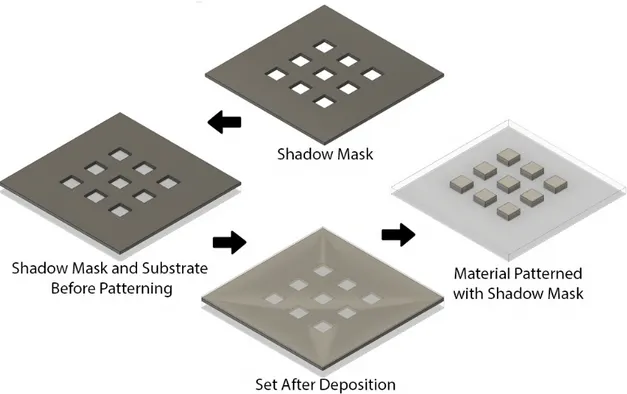
A shadow mask can be a simple laser-cut sheet, a metal mask, or a silicon-based shadow mask, its use will be dependent on the resolution and patterning accuracy that is needed. A laser-cut sheet can offer a simple and cost-saving way of patterning using shadow mask technology at the expense of resolution being dictated by the laser precision. On the other hand, a high-resolution metal mask can offer a micron resolution with sub-micron tolerances at a higher cost. Have already been produced stainless steel shadow mask using a combination of micro-electro-discharge machining and electrochemical etching, obtaining 95 µm of thickness, a wall with 3.6 µm in width and, 150 µm in length, which corresponds to an aspect ratio of around 1/26 [7]. Regarding silicon-based masks, it has been proven to be possible to make shadow masks using laser-interference-lithography in silicon nitride with silicon as support achieving resolution as low as 120 nm [4, 8]. Using silicon has a shadow mask features of 500 nm can be achieved with great reliability, being reutilized at least 20 times [3]. For silicon nitride, direct milling focused ion beam was proven to be efficient [9]. For the fabrication of these masks it is used wafer-through etching solutions that make it possible to create a thin layer where it is designed the shadow mask pattern.
In order to pattern devices, an alignment strategy is required,such as using of metal rods to guide to the substrate holder. When the rods are placed, and it is all aligned the mask is bolted to the holder having the substrate in between in order to pattern it. The possibility of using an equipment composed by holders and microscope to assure the correct positioning of the mask and substrate has also been proposed and developed [10, 11].
This method of patterning may be affected by clogging, which means that the material being deposited will do so on the substrate and the mask, this leads to the decreased size of the features. After each use, the masks should be cleaned with a selective etchant to the material being deposited [5].
When using a thin membrane as a shadow mask the deposited materials may induce mechanical stress. This can lead to a change in the feature size because the details are being forced to maintain a position that is not the desired one. It is possible to stabilize the membrane using localized reinforcement structures [12].
1 . 3 . PA RY L E N E - C S H A D O W M A S K S S TAT E O F T H E A R T
1.3
Parylene-C Shadow Masks State of the Art
Parylene or poly(p-xylylene), is a polymer that offers its applicability in different fields due to its properties. This material shows compatibility with microfabrication processes, chemical inertness, and biocompatibility. When used as a coating has a stress-free con-formal deposition, low defect count, mechanical flexibility and a large linear elastic range [13–17]. The only feasible and practical way to pattern Parylene is by using oxygen plasma [18]. Parylene is applied as a coating to encapsulate and passivate PCB, connec-tions, MEMS devices, and biomedical devices. It is not commonly used as a structural or substrate material for electronic or MEMS but it is amply used in the devices [19–22]. There are several types of Parylene the most used types are Parylene-N, Parylene-C, and Parylene-D, as shown in figure 1.1.
Figure 1.1: Parylene types. Adopted from [23].
Parylene-C is deposited by chemical vapor deposition, this deposition occurs in three stages, dimer vaporization, pyrolysis to form monomers and polymerization. The process is normally done under vacuum, at 16 mBar or less, to assure that it does not occur contamination [13]. During the deposition a thin film of parylene-C is formed, and the dimer mass used will determine the thickness of the produced film.
With these thin membranes, it was already possible to fabricate shadow masks with a high aspect ratio etching. This means that in a 55 µm thick film it was able to etch through a 6 µm opening, resulting in an aspect ratio of 1/9. This was intended to be used for pat-terning cells and proteins and it was successfully made in polystyrene and methacrylate glass surfaces. To pattern proteins the shadow masks are attached to the substrate, the proteins bond with the substrate, the excess is removed with a buffer solution and the shadow mask is removed leaving the proteins where desired [24]. Parylene-C stencils have been used for patterning proteins and cells [25] to generate patterned co-cultures [26].
When trying to pattern curved surfaces of PDMS with aluminum the results showed that the sheet adhered to the surface with a well-defined pattern [27].
Using a parylene-C/Cr shadow mask the smallest feature obtained was 3 µm and this mask maintains its patterning capability for at least 6 depositions. This material
C H A P T E R 1 . I N T R O D U C T I O N
combination is interesting by the fact that parylene-C and Chromium have a similar thermal expansion coefficient, which is important when two thin films are in contact with each other because the temperature affects them similarly, causing their expansion at the same rate and it will not cause the whole structure to bend and curl on itself [28].
Mechanical alignment techniques are important by the fact that shadow mask technol-ogy is most of the times limited to single-step patterning so in this matter the approach was to create structures that could hold in place all the used masks, this was tested using alignment pillars made from SU-8, negative photoresist, that is deposited on the wafer by spin coating and after its baking, exposure and development procedures the pillars are created [29]. The results obtained using this method show that by depositing two times the same E shaped structure, the misalignment can vary between 4 and 9 µm, doing it on top of each other or in front of each other [27, 30].
1.4
Parylene-C Shadow Mask Considerations
Fabrication
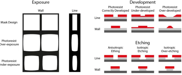
During the several steps of the shadow mask fabrication, there may occur errors, that will lead to a deviation on the detail dimensions. The feature definition can be compromised in the fabrication steps that include material removal. These errors may come from the lithography process, where the photoresist details do not become the expected size, the same may happen during the metal hard mask and the parylene-C erosion. Over exposing, developing and etching will cause the walls, spacing between two features, to be slimmer than expected and the lines will be larger. Under exposing, developing and etching will cause the walls to be larger and the lines to be slimmer [31, 32].
Figure 1.3 shows how the final pattern is affected during the procedure.
Figure 1.2: Feature size deviation. 4
1 . 4 . PA RY L E N E - C S H A D O W M A S K C O N S I D E R AT I O N S
The deviation can occur as well if the mask that is being fabricated has different lines and wall sizes, the smaller details will require less time during the etching steps and they may be over etched while the bigger details are as desired, assuming a constant ratio on the sample area.
Device Patterning
Shadow masks are applied to pattern thin-film transistors, capacitors, diodes and many other electrical components. In some cases, it is simpler than using the photolithographic procedures that can be more expensive and time-consuming. To deposit the different layers the mask is used as exemplified in figure 1.3.
Figure 1.3: Shadow mask usage procedure.
As an example, a TFT device requires four different depositions, one for the source and drain contacts, one for the semi-conductive layer, one for the dielectric layer, and one for the gate contact [33]. A capacitor device will require three layers, two contacts that are overlapping, and a dielectric material layer [34].
C
h
a
p
t
e
r
2
M a t e r i a l s a n d M e t h o d s
2.1
Production Techniques
Parylene-C DepositionThe equipment used for the parylene-C deposition was PDS (Parylene Deposition System) 2010 LABCOTERTM 2 by Specialty Coating Systems. The deposition process occurs in three stages. Firstly vaporization, where the used dimer will reach the vapor state around 90° C and to control the vaporized gas, the vaporization chamber can reach up to 175°C. Secondly pyrolysis, where the parylene gas is decomposed into monomers at the temperature of 690°C. Thirdly the deposition step occurs at ambient temperature and pressure under 16 mBar, the monomers move into the chamber and polymerize onto the substrate and it is formed a thin polymeric film. During this work the produced membranes had thickness of 3 µm and 5 µm, which corresponds respectively to 5 g and 10 g of parylene-C dimer mass.
Polyvinyl Alcohol Solution
PVA solution is used as a sacrificial water soluble layer that will allow to peel-off parylene membranes from a carrier. The solution was prepared using water and polyvinyl alcohol with 20.000 to 30.000 repetition units as precursors. The chain length was the smallest available for an easier dissolution. The solution concentration was 5 wt.%. To improve the dissolution the flask used was placed in heat and rotation. The temperature used in the hot plate was 100 ° C and agitation at 800 rpm. The PVA was added in small amounts to make sure that all the powder was dissolved.
C H A P T E R 2 . M AT E R I A L S A N D M E T H O D S
Aluminum Wet Etching Solution
The wet etching solution allows removing chemically part of a film that is exposed to the etching solution. The solution used to remove aluminum is composed of phosphoric acid, nitric acid and deionized water with a concentration of 85% and 65%, for the acids respectively, and proportions of 65%, 6%, and 29%, respectively. Phosphoric acid is used to etch the native aluminum oxide, acetic acid is used to improve the wetting of the substrate and water is used to adjust the etch rate.
Reactive Ion Etching
The equipment used for reactive ion etching is a Minilock – Phantom RIE from Trion Technology. Dry etching using O2 plasma is used to etch parylene-C layers. This tech-nique allows achieving an anisotropic etching, which means that the parylene-C will only be etched where it exposed. The set values used were the temperature is at 25 ° C, O2
flow of 50 sccm, RIEFW power of 50 W, and pressure of 0.067 mBar. The etching time is dependent on the parylene layer thickness, but the etching ratio is around 0.275 nm/sec. Photolithography
For photolithography the mask aligner used was a Karl Suss MA-6 and the used photore-sist was AZ 6632. The photorephotore-sist application is done by spin-coating, the optimized parameters are 10 s at 1500 rpm followed by 20 s at 3000 rpm. The curing process is done at 115° C during 75 s, and it assures that the solvents do evaporate. The exposure is done in the mask aligner, where the mask is between the sample and the UV light. The exposure time under UV radiation is 30 seconds, optimized having in account the UV lamp power, and the irradiated parts of the positive photoresist turn soluble in a developer solution, the photoresist AZ 6632 is removed by the developer AZ 726 MIF or AZ 400K, and the sample is then passed through water to stop the development process. Thermal Evaporation
Thermal evaporation was used to deposit aluminum. For the deposition, a high current, between 50 and 60 A is applied on a tungsten crucible containing aluminum rods, making it evaporate, and a thin film formed on the substrate. The system is under vacuum, the deposition occurs at pressures inferior to 3×10⁻⁶mBar. The whole process is controlled by a quartz crystal that given the density, 2.7 g/cm3and acoustic impedance, 8.2 ×10⁵g/cm2s for aluminum, can estimate the thickness and deposition rate.
2 . 2 . C H A R AC T E R I Z AT I O N T E C H N I Q U E S
Sputtering
The sputtering equipment used is from Aja, International. This technique was used to deposit GIZO (Gallium Indium Zinc Oxide) and Molybdenum. The parameters that were kept constant are the distance between the target at 35 cm and the substrate, the temperature at ambient temperature, and the target size at 7.62 cm of diameter. The deposition parameters are presented in table 2.1.
Table 2.1: Sputtering conditions.
Material Gases and Flow Pressure (Pre)Sputtering Time RF Power Thickness
sccm mBar min W/cm2 nm
GIZO O214 and Ar 2 3.1×10⁻³ (10) 12 14.2 20
Molybdenum Ar 40 2.3×10⁻³ (5) 13 24.7 60
2.2
Characterization Techniques
Optical Microscopy
This technique allows to inspect and measure the size of the features in the parylene shadow mask, and it was used during all the steps to assure that all had gone as expected. The equipment used was an Olimpus BX51, and the program used to measure was Image-J.
Profilometer
The profilometer was used to determine the thickness of the produced films and struc-tures to compare with expected thickness, it was used to measure parylene-C films, pho-toresist pillars and SU-8 pillars. The equipment used is an AMBIOS XP-200.
C
h
a
p
t
e
r
3
R e s u lt s a n d D i s c u s s i o n
3.1
Shadow Mask Fabrication and Usage
3.1.1 Shadow Mask Fabrication Protocol
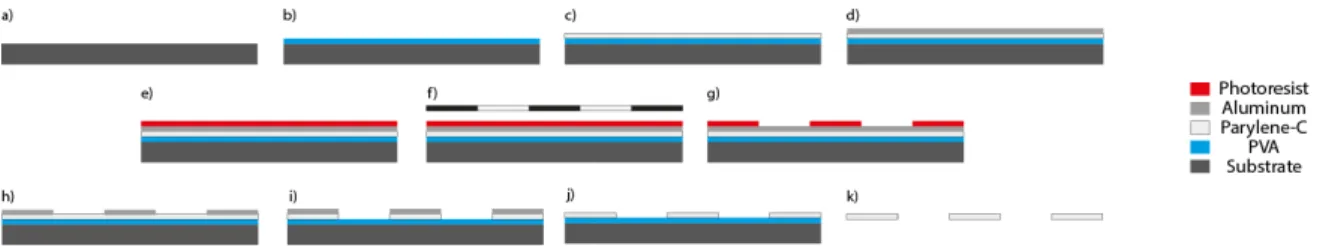
One of the objectives of this work was the production of a protocol for the fabrication and use of these parylene-C thin membranes as shadow masks. The shadow mask fabrication is graphically explained in figure 3.1, where it is possible to see what materials were used and what is their function in this process.
Figure 3.1: Shadow mask fabrication steps.
The parylene-C shadow mask fabrication follows these steps:
Step a) Substrate cleaning: The substrate cleaning is done in three steps, acetone bath, isopropyl alcohol (IPA) bath, and water bath, in ultrasounds for ten minutes each. Step b) PVA deposition by spin-coating: A PVA thin film is deposited by spin-coating, 1000 rpm for 1 minute and annealed at 95°C for 5 minutes, this layer will act as a sacrifi-cial layer in order to remove afterward the parylene from the substrate.
Step c) Parylene-C deposition: Material used for the shadow mask. Membranes of 3 µm and 5 µm were produced during this work.
C H A P T E R 3 . R E S U LT S A N D D I S C U S S I O N
Step d) Aluminum deposition: Material used as a hard mask for the dry etching proce-dure.
Step e) Photoresist application: The photosensitive material is deposited by spin coating. Step f) UV exposure: The sample is put in contact with a photolithography mask, using a mask-aligner, that will cover some parts of the sample, knowing the UV lamp power the exposure time is calculated and the non-protected parts of the sample are exposed to UV radiation.
Step g) Photoresist development: A pattern is defined in photoresist on top of the alu-minum layer, the photoresist exposed to UV radiation, in the case of using positive pho-toresist, will be dissolved in the developer solution.
Step h) Aluminum wet etching: The aluminum parts that are not protected by photoresist will be removed by an etching solution. The solution is composed of phosphoric acid, nitric acid, and water.
Step i) Parylene-C dry etching: After the aluminum etching, some parts of the parylene layer are exposed and are etched completely by an oxygen plasma.
Step j) Aluminum removal: The aluminum on top of the parylene-C layer causes the membrane to curl on it self due to thermal expansion and stress effects. To avoid damag-ing the shadow mask it is important to remove the aluminum.
Step k) Shadow mask peel-off: When in contact with warm water the PVA layer is dis-solved resulting in the parylene layer being released from the silicon substrate. This stage was tested using PVA and photoresist as a sacrificial layer, using different spin-coating and annealing, the one with the best results was the PVA with annealing. To make sure that the mask was cleaned and dried with a nitrogen stream while in between clean-room wipes. To store the masks and make sure they were as flat as possible it was laser cut a 75 µm thick kapton support where the mask would rest.
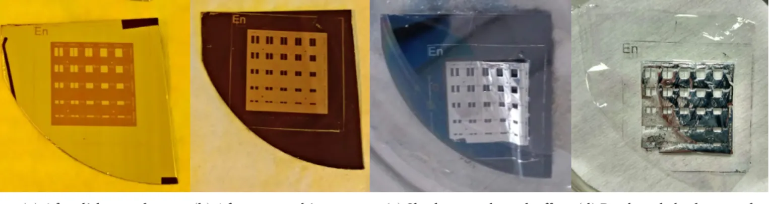
(a) After lithography. (b) After wet etching step. (c) Shadow mask peel-off. (d) Produced shadow mask.
Figure 3.2: Fabrication steps of a 3 µm parylene-C shadow mask.
3 . 1 . S H A D O W M A S K FA B R I C AT I O N A N D U S AG E
Figure 3.2 has the different stages of fabrication from one of the masks produced during this work. Figure 3.2 (a) shows a silicon carrier with a PVA layer, a parylene-C layer and an aluminum layer after photolithography, where it was defined a pattern in photoresist. Figure 3.2 (b) is the same sample after the wet etching step, where the aluminum layer is etched where the photoresist is not protecting it. Figure 3.2 (c) shows the shadow mask peel-off, the PVA layer is dissolved in water bath. Figure 3.2 (d) presents the produced 3 µm shadow mask.
3.1.2 Shadow Mask Design
When working with thin and flexible membranes its mechanical stability must be take into account. Therefore the density of details (opening on the mask) should be reasonably low and the borders of the mask should be avoided to allow the handling of the mask. Photolithography masks were used and adapted for the shadow mask fabrication. For this, some parts of the mask were covered during the photolithography procedure or during the dry etching procedure. The critical dimensions commonly studied are the line width, feature distances (walls), and feature size. During this work, the main focus was on the fabrication of walls and lines.
3.1.3 Sample Holder Development
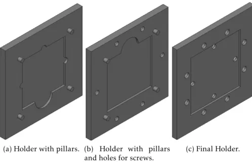
To use the produced shadow masks as patterning tool in a substrate, there was the need to develop a sample holder to fix both the sample and the mask. The holder develop-ment had some prototype designs until the final one was done and fitted all the neces-sary requirements, all were designed using Fusion 360 and printed in a 3D printer. For prototyping the used material was PLA, for the final holder the chosen material was a high-temperature resistant resin, since during the depositions other materials could not resist the temperature. The objective of the holder is to have the substrate fixed, using substrates of 2.5 cm by 2.5 cm, and to have the parylene mask in contact with it in the right position, being fixed as well. Figure 3.3 shows some of the different designs tested for the holder.
Initially the mask was fixed using the holder pillars and in the more recent versions, the mask was secured with nuts and screws. A similar optimization was performed to maintain fixed the sample, holding it with screws.
For being able to use different thickness substrates the depth of the base is 1 mm to accommodate glass substrates and also Si/SiO2 substrates ,using a base to compensate
the height. The shadow mask needs to be standing on the surface of the substrate.
C H A P T E R 3 . R E S U LT S A N D D I S C U S S I O N
(a) Holder with pillars. (b) Holder with pillars and holes for screws.
(c) Final Holder.
Figure 3.3: Substrate and shadow mask designed holders.
3.1.4 Shadow Mask Use
Device patterning using parylene-C shadow mask follows these steps: 1. Insert the clean substrate on the holder.
2. Place the shadow mask on top of the substrate making sure it is as spread and flat as possible.
3. Material deposition through the parylene-C shadow mask apertures. Figure 3.4 has these steps exemplified.
Figure 3.4: Holder(left), holder and substrate (middle), set ready for material deposition (right).
The shadow mask is quite difficult to handle due to its thickness. To simplify this task a laser cutted kapton frame was used, allowing for a better alignment of the mask in the holder.
3 . 2 . S I N G L E - S T E P PAT T E R N I N G
3.2
Single-Step Patterning
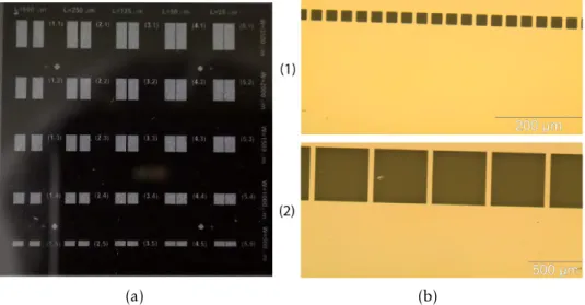
The fabrication and testing of the parylene-C shadow masks started with single-step patterning. This means that the shadow mask is used for one deposition in each substrate to pattern the desired details. The photolithography masks used for this stage of the work are both used to pattern electrical contacts. The photolithography masks used in this stage of the work are presented in figure 3.5.
(a) (b)
Figure 3.5: Single-step patterning lithography masks (a) rectangular contacts mask, (b) square contacts mask (1) 10µm spacing squares with 25 µm dimensions (2) 50µm spacing squares with 500µm dimensions.
Rectangular contacts mask has rectangular contacts, grouped in pairs,with constant width of 1 mm and lengths of 2.5 mm, 2 mm, 1.5 mm, 1 mm or 0.5 mm. The separation changes and it is 500 µm, 250 µm, 125 µm, 50 µm or 25 µm.
Square contacts mask has lines of squares with dimension of 500 µm, 250 µm, 100 µm, 50 µm, and 25 µm, with different separation between them of 50 µm and 10 µm.
3.2.1 Shadow Mask Characterization
The characterization is crucial when producing these shadow masks so that it can be de-termined the attainable resolution, smallest feature that can also be produced to achieve a high yield, and how efficient is the reproducibility of patterns. To characterize the shadow mask features it is necessary to analyze first the mask that it originates from.
To simplify the reading on this and on the following graphics, the following nomen-clature was used:
• Design ratio - Ratio between the dimensions of the lithography mask and the theo-retical design.
• Fabrication ratio - Ratio between dimensions of the shadow mask and the pho-tolithography mask.
C H A P T E R 3 . R E S U LT S A N D D I S C U S S I O N
Rectangular Contacts Mask
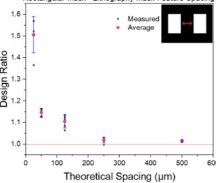
The first step in the characterization is the photolithography mask analysis. In figure 3.6 the design ratio results for the spacing between the features in the rectangular con-tacts acetate film photomask are presented as well as the average and standard deviation values.
Figure 3.6: Rectangular contacts lithography mask spacing design ratio.
There is a tendency and it shows that for the smaller spacing the mean value is further away from the theoretical value and standard variation is larger, while for larger features the mean value is closer to the theoretical value. For a theoretical spacing of 25µm, the average was around 37µm, while for 500 µm the average was around 507µm. This means that even though the theoretical maximum resolution from the photolithography mask was 25 µm the produced mask has a 37 µm minimum feature dimension, this dimension will be responsible for the patterned thin film features.
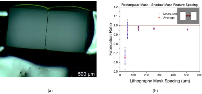
This acetate film photomask was then used to transfer the pattern to a 3 micrometer thick parylene-C shadow mask, which can be seen in figure 3.7 (a), using the proce-dure already mentioned. Figure 3.7 (b) presents the results from the fabrication ratio, shadow mask/ lithography mask dimensions, of spacing between contacts in the pro-duced shadow mask, using the rectangular contacts photolithography mask.
The presented results are from a single produced mask were during the fabrication all the 25 pairs of contacts were produced successfully in this mask, and the sacrificial layer used was PVA annealed at 95 ºC during 5 minutes. There were other three masks produced, using different conditions for the sacrificial layer used for the peel-off, where the details that the final mask had were 76% yield using a photoresist double layer, 80% yield using photoresist, and 88% yield using PVA without annealing. The yield is the number of details that were not destroyed during the peel-off divided by the number of details in the mask.
3 . 2 . S I N G L E - S T E P PAT T E R N I N G
(a) (b)
Figure 3.7: Produced rectangular contacts shadow mask (a) 25 µm theoretical detail, (b) spacing fabrication ratio results.
Having the photolithography masks as a reference all the average spacing details are smaller, which means that during the fabrication the produced walls are thinner than expected so it occurred over-exposure, over-development or over-etching. This is mainly caused by the aluminum wet-etching and the parylene-C etching stages.
Square Contacts Mask
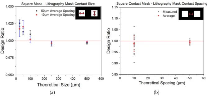
The square contacts photolithography mask used was fabricated using the original quartz mask and inverting the design for its negative, the one need for the shadow mask fabrica-tion. In figure 3.8 is presented the design ratio for spacing and size of the features in the square contacts mask.
In this mask, the spacing between contacts and its dimension are related, and the increase of one means necessarily the decrease of the other. Regarding the contact size results all the results are near the theoretical value, being the maximum attainable reso-lution average for contact size 25.5 µm. The average for the contacts spacing resoreso-lution is 9.8 µm and 49 µm.
After this analysis the photolithography mask was used to produce two parylene-C shadow masks with 3 µm of thickness that can be seen in figure 3.9.
C H A P T E R 3 . R E S U LT S A N D D I S C U S S I O N
(a) (b)
Figure 3.8: Square contacts lithography mask design ratio (a) for size and (b) spacing.
(a) 10 µm spacing shadow mask. (b) 50 µm spacing shadow mask.
Figure 3.9: Produced square contacts shadow masks.
In figure 3.10 the results from the produced shadow masks using the square contacts photolithography mask are presented. The variable used to characterize the shadow mask production is the fabrication ratio.
Analyzing the results it is concluded that the contact size is smaller than intended and the spacing larger. This means that during the shadow mask fabrication there was under-exposure, under-development or under-etching. This was mainly caused by the aluminum under-etching.
3 . 2 . S I N G L E - S T E P PAT T E R N I N G
(a) (b)
Figure 3.10: Square contacts shadow mask fabrication ratio for (a) size and (b) spacing.
3.2.2 Parylene-C Shadow Mask Patterning
To test the produced shadow masks they had to be used for patterning and since the masks were characterized it is possible to compare the patterned contacts with all the masks that were used during this process. For such, aluminum was evaporated and patterned using these shadow masks in a glass substrate, using the developed substrate holder. The graphs related to patterning are quantified using a pattern ratio, this ratio is the quotient between the dimension in the patterned detail and the shadow mask dimension.
Figure 3.11 (a) has the results from patterning using the rectangular contacts shadow mask, using as a reference the shadow mask used to pattern the contacts. Figure 3.11 (b) shows a pair of contacts with 25 µm of spacing between each other.
Analyzing the data present in the graph it can be concluded that for all contacts spacing the average pattern ratio is under the unit reference, where the detail patterned is equal to the one in the shadow mask. This indicates that the features produced are larger than the openings in the mask suggesting that aluminum was also deposited under the mask.
Even so the results from the 25 µm, 250 µm and 500 µm are close to the unit, with a maximum deviation of around 2.5 %, which is a good patterning performance for the parylene-C shadow mask. For the 50 µm and 125 µm the results are not as impressive and this can be cause by the mask not being as completely adhered to the substrate when patterning, causing the features to became smaller than desired.
C H A P T E R 3 . R E S U LT S A N D D I S C U S S I O N
(a) (b)
Figure 3.11: Rectangular contacts pattern ratio results (a). Contacts spaced by 25 µm and length of 2.5 mm patterned using parylene-C shadow mask (b).
Sputtering vs Thermal Evaporation
To test the square contacts shadow masks, it was deposited through the using thermal evaporation and RF magnetron sputtering in order to compare how the features patterned dimensions are influenced by the deposition technique. Sputtering has a better step cov-erage than thermal evaporation due to the higher kinetic energy of the sputter atoms that leads to a surface diffusion and a more conformable deposition. Therefore the patterning of thin gaps using shadow masks is more challenging since any under mask deposition or spreading may compromise the gap definition. Aluminum was thermal evaporated and deposited through the masks with 50 µm and 10 µm of contact spacing, molybdenum was only sputtered through the 50 µm spacing mask.
Some of the details patterned using the square contacts shadow masks are shown in figure 3.12.
(a) Aluminum patterned square contacts with 50 µm spaced by 50 µm.
(b) Molybdenum patterned square contacts with 100 µm spaced by 50 µm.
Figure 3.12: Patterned square contacts using parylene-C shadow masks. 20
3 . 2 . S I N G L E - S T E P PAT T E R N I N G
The graphs in figure 3.13 have the results regarding the patterning using the square contacts shadow masks.
(a) (b)
Figure 3.13: Patterned square contacts (a) spacing and (b) contact size pattern ratio. Figure 3.13 (a) graph shows the contact spacing value. Analyzing the results it can be found two different behavior. For the theoretical 50 µm spacing features deposited with aluminum in average maintained the same size as previously analyzed in the produced shadow mask. For the features with theoretical 10 µm patterned with aluminum and the 50 µm features patterned with molybdenum in average the contact spacing decreased meaning that in some degree material was deposited under the shadow mask.
The observed contact spacing between features in sputtered molybdenum films are smaller than the shadow mask spacing. This is the expected result due to the more conformable nature of the deposition. The fact that is smaller than the mask separation indicates the material spreading due to a non zero gap between mask and substrate surface [35].
To summarize the spacing patterning results, in table 3.1 are presented the obtained average results for the different masks and techniques used. The variation column presents in percentage the difference between the shadow mask and the patterned size divided by the shadow mask average feature size, if the value is positive the detail is smaller then the shadow mask, if negative larger.
C H A P T E R 3 . R E S U LT S A N D D I S C U S S I O N
Table 3.1: Comparison between sputtering and thermal evaporation defining spacing. Spacing (µm)
Masks Thermal Evaporated Aluminum Sputtered Molybdenum Lithography Mask Shadow Mask Patterned Variation(%) Patterned Variation(%)
51.0 56.3 53.0 5.9 49.0 18.2
9.9 12.5 10.3 13.0 -
-Figure 3.13 (b) graph has the contact size pattern ratio. Following the same principle and having in mind the relation between the spacing between contacts and the contact size data the contact size was also analyzed.
For contact size larger than 50 µm the pattern ratio results from the three depositions are in the 5% range deviation from the shadow mask size. For contact size equal to 50 µm the the 50 µm spacing depositions were successful but for the 10 µm spacing mask the contact size is larger than the shadow mask. For contact size smaller than 50 µm the pattern ratio results from the three depositions are smaller than the unit, which means that the pattern contact is smaller than the one in the shadow mask.
To summarize the contact size patterning results, in table 3.2 are presented the ob-tained average results for the different masks and techniques used.
Table 3.2: Comparison between sputtering and thermal evaporation defining contact size. Contact Size (µm)
Masks Thermal Evaporated Aluminum Sputtered Molybdenum Lithography Mask Shadow Mask Patterned Variation (%) Patterned Variation (%)
498.9 486.8 486.2 0.1 -
-249.1 241.5 246.6 -2.1 254.3 -5.3
100.1 95.4 95.0 0.3 97.1 -1.9
50.8 46.0 52.5 -14.0 52.0 -13.1
25.5 20.0 18.7 6.6 21.6 -8.0
Combining both results, spacing and contact size, it is concluded that in general most of the squares dimensions were enlarged and the spacing was decreased, meaning that some material was able to be deposited under the mask, this can be caused by non-zero gap between the shadow mask and the substrate surface.
Overall the technique that shows better usability for these shadow masks is thermal evaporation with aluminum because the shadow mask feature size is better replicated using it. The sputtered molybdenum results are closer to the photolithography mask, this means that the material is being deposited under the shadow mask. This effect can be improved by a better adhesion, ensuring that the gap between the shadow mask and the substrate is zero in the whole surface leading to a smaller detail size difference.
3 . 2 . S I N G L E - S T E P PAT T E R N I N G
Single-Step Patterning Summary
To summarize the single-step patterning results in table 3.3 and 3.4 are presented the obtained average results for the different details studied. The shadow mask variation has the lithography mask as reference and the patterned contacts have the shadow mask as a reference. The variation is calculated by the difference between the average and its reference divided by the reference average.
Table 3.3: Patterned contacts size using a produced shadow mask. Contact Size (µm)
Lithography Mask Shadow Mask Variation(%) Patterned Variation(%)
498.9 486.8 2.4 486.2 0.1
249.1 241.5 3.1 249.1 -3.1
100.1 95.4 4.7 95.7 -0.3
50.8 46.0 9.4 52.3 -13.7
25.5 20.0 21.6 19.6 2.0
Table 3.4: Spacing between patterned contacts using a produced shadow mask. Contact Spacing (µm)
Lithography Mask Shadow Mask Variation(%) Patterned Variation(%)
507.7 487.2 4.0 485.4 0.4 254.9 246.4 3.3 240.4 2.4 138.1 134.4 2.7 126.6 5.8 51.0 56.3 -10.4 51.4 8.7 37.7 24.8 34.2 24.1 2.8 9.9 12.5 -26.3 10.3 17.6
Single-step patterning was tested already in other papers and the best results achieved were squares with 15µm × 15 µm, lines with width of 25 µm and 15 µm of separation between each other [27].
The obtained results showed that are details in all the phases that must be had in account for the production and application of this thin membranes as shadow masks, mainly a rigorous control in the photolithography and etching steps regarding the mask production and the mask adhesion to the substrate during patterning. Having tested these shadow masks and having the understatement of what was happening during the fabrication and patterning steps it started the application of what was learned in device fabrication.
C H A P T E R 3 . R E S U LT S A N D D I S C U S S I O N
3.3
Multi-Step Patterning
When trying to produce devices there is the need to align different material layers with each other. The masks used for this stage of the work were based on TFT devices where the principal parameters explored were the source and drain separation and the gate width. To make a TFT device the source and drain separation has to be positioned in line with the gate. In a shadow mask the source and drain contacts will form a wall between each other, and the gate contact is a line.
The results and habits learned in the single-step patterning stage of this work were used and implemented to optimize this one.
3.3.1 Mask Design
The masks used in this stage of the work were designed to produce TFT devices, the photolithography masks were printed in acetate film photomasks, in which the maximum resolution obtained for walls was 20 µm and for lines 15 µm. The software used for the photolithography mask design was Adobe Illustrator.
(a) Initial design. (b) Test design. (c) Reproducibility design.
Figure 3.14: Multi-step patterning designed masks.
The mask design started with the first TFT mask, figure 3.14 (a), the four masks are intended to pattern devices with a width of 1 mm and length of 50µm and 20µm. The holes in the corners were implemented to try the alignment.
The test design, figure 3.14 (b), was designed to test a different width and length in each device. The width is 100 µm, 75µm, 50µm, 25µm or 20 µm and the length is 50 µm, 40 µm, 30 µm, 25 µm, 20 µm or 15 µm.
The reproducibility design, figure 3.14 (c), was designed to test four different sizes of transistor to see if the properties are maintained in the nine of each size. The width is 100 µm or 50 µm and the length is 50 µm or 25 µm.
The masks can be seen in more detail in the annexes, annex 1 has the initial design, annex 2 has the test design and annex 3 has the reproducibility design.
3 . 3 . M U LT I - S T E P PAT T E R N I N G
When patterning TFT devices the gate width must include a safe overlapping width to assure a misalignment margin Ideally the gave overlap with the source and drain contacts should be minimum to avoid parasitic effects. In the final design a margin of 20 µm in the line width was added to ensure a viable gate-source and drain alignment even if some mask misalignment occurs. The design was implemented to test the possibilities of this material as a shadow mask, and if it works in this designs it will work as well in optimized designs.
3.3.2 Alignment Strategies
The alignment stage was tried using three different approaches, manual alignment with the initial design, photoresist pillars with the test design, and SU-8 pillars with the repro-ducibility design. To keep the substrate in place and to hold the mask it was developed alongside the masks a 3D holder like the one presented in figure 3.15.
Figure 3.15: Designed holder for patterning flat substrates.
The yield of the devices is determined by the contacts depositions,since this is the crit-ical dimension in shadow mask patterning. A device is considered successfully patterned if the the source-drain contacts are not in short circuit and if they are aligned with the gate.
Manual alignment
The manual alignment was tried with the initial TFT mask set. This mask has holes in the corners that are inserted in the designed holder with pillars with the same size, as seen in figure 3.16.
The first deposition was done defining the source and drain contacts and then it was tried the alignment by manually inserting the gate apertures in between the previously deposited contacts.
C H A P T E R 3 . R E S U LT S A N D D I S C U S S I O N
Figure 3.16: Mask alignment with the substrate and holder.
The results achieved with this approach are surprising since this is the less rigorous way tested to align. Using this methodology was possible to align lines of 40 µm with apertures of 20 µm. Figure 3.17 shows that the alignment was attained successfully in the x axis and it needed to be improved is the y axis in order to achieve the desired alignment.
(a) W=1 mm, L=20 µm. (b) W=1 mm, L=50 µm.
Figure 3.17: TFT initial mask set manual alignment between source and drain and gate. For this method of alignment the obtained yield was 6 from the 36 devices patterned, achieving an alignment between all the layers.
Photoresist pillars
The photoresist pillars were used for alignment in the test TFT mask set. The mask has an array of 5 × 5 circular holes with 500 µm of diameter that were aligned with 4 µm thick photoresist pillars, measured using a profilometer. This mask has 3 µm of thickness. The concept behind this alignment try was to use a material that could be easily be patterned into a substrate that was around the thickness of the mask since the idea is to pattern while the shadow mask is as close as possible from the substrate, ideally in complete contact with the whole surface.
3 . 3 . M U LT I - S T E P PAT T E R N I N G
(a) Pillar and mask alignment before the first deposition.
(b) TFT misalignment.
Figure 3.18: Tests with photoresist as alignment.
Figure 3.18 (a) shows the mask aligned with a photoresist pillar before the first mate-rial deposition. This observation is important to assure that the set is ready for patterning. As seen in figure 3.18 (b) this alignment try was not as successful as initially was though since the last patterning step, the source and drain deposition, missed in one of the axis completely the objective. This was caused by the use and reuse of the pillars and this lead to their abrasion and made the last step of patterning being catastrophic for the devices.
SU-8 pillars
The SU-8 pillars were used for alignment in the reproducibility TFT mask set, the mask has a 5 × 5 array of circular holes with 500 µm of diameter that were aligned with 33 µm thick pillars, measured using a profilometer. This mask has 5 µm of thickness. SU-8 is a negative photoresist and the application has more steps than using conventional photore-sist. The alignment procedure taken was equal to the one taken with the photoresist but this time the pillars are thicker, about seven times the thickness of the mask. Figure 3.19 (a) shows one of the SU-8 pillars and figure 3.19 (b) shows the set ready for patterning.
(a) SU-8 pillar. (b) Gate mask ready for patterning.
Figure 3.19: Alignment using SU-8 pillars. 27
C H A P T E R 3 . R E S U LT S A N D D I S C U S S I O N
Using this method the results were the better from the three methodologies used and all of the devices gates were lined up with the source and drain separation, from the ones that the mask had well defined. This proved to be the most effective way to aligned the shadow masks from the three that were experimented, as can be seen on figure 3.20 the TFTs from both of lengths achieved a good alignment.
(a) TFT with L=25 µm. (b) TFT with L=50 µm.
Figure 3.20: Tests with SU-8 pillars as alignment.
For this method of alignment the obtained yield was 28 from the 30 devices patterned, achieving an alignment between all the layers. In this instance there are only counted 30 devices to be possible patterned because of the mask fabrication were only 30 out of 36 were well defined in the source and drain shadow mask.
Alignment Summary
The holder and mask design evolved with the different details that were added to each other to make a set that was possible to pattern with. The TFT designs that were test allowed to make devices with W/L ratios ranging from 0.75 to 50.75, depending on the semiconductor deposition. In short it was possible to pattern four different material layer to pattern TFT devices, being the best method the use of SU-8 pillars to align the shadow masks with the substrate.
Multi-step patterning using SU-8 posts as an alignment strategy was tested already in other papers and the best results achieved were misalignment between 4 µm and 9 µm using 100 µm and 250 µm thick posts [27].
3 . 4 . C U RV E D S U R FAC E PAT T E R N I N G
3.4
Curved Surface Patterning
To pattern in fibers using conventional photolithography, it is not as simple as when patterning in flat surfaces. Mainly because of the photoresist application and its exposure. The exposure will not be homogeneous because of the variation in height of the sample, in the middle the sample is closer to the mask and on the sides is farther away. Having this in mind the parylene-C shadow masks were designed to make possible the patterning possible in this kind of curved surface. The principle behind pattering with these shadow masks is to wrap the fiber with it, patterning only where the mask is open. In order to do this a fiber holder was designed, figure 3.21, and it must be able to immobilize the fiber and make the mask rest on it.
Figure 3.21: Designed holder for fiber patterning.
3.4.1 Mask Design
The purpose of the designed masks in this stage of the work is to pattern capacitors, as can be seen in figure 3.22. For this, there are there materials layers required, two electrical contacts and one dielectric material. The design has two circles with diameter of 1 mm and square pads of side 500 µm of to make electrical contact. The device will work by the fact that there is an overlap of electrical contacts with a dielectric material in between. The two holes on each side were implemented in order for the mask to be aligned with fiber, which is fixed in the holder pillars, where the two holes are inserted. The mask is then wrapped around the fiber and it is ready to be patterned.
Figure 3.22: Designed masks for capacitors, bottom contact (left), dielectric material (middle), top contact (right).
C H A P T E R 3 . R E S U LT S A N D D I S C U S S I O N
3.4.2 Capacitors in Fibers
To fabricate the capacitors it was first deposited a 90 nm thick film of aluminum through the produced shadow mask, then it was deposited around 200 nm of parylene-C to serve has dielectric material and then it was deposited a second layer of 90 nm of aluminum. Figure 3.23 (a) presents the holder, the fiber and the shadow mask ready for the top contact deposition. Figure 3.23 (b) shows one patterned capacitor and it is perceptible that the device was successfully patterned.
(a) Fiber in the holder. (b) Capacitor in fiber.
Figure 3.23: Patterned capacitor in a fiber.
To pattern these capacitors it is necessary that the mask is wrapped around the fiber, if it is not the result will be the same as having a conventional shadow mask making the patterning because the material being deposited will miss the fiber and get deposited in the holder. In this case, the fiber was patterned around 42% of the whole perimeter. The maximum possible to pattern would be 50% of the perimeter since the rest of the fiber is impossible to pattern having the fiber set up like this.
C
h
a
p
t
e
r
4
C o n c lu s i o n s a n d F u t u r e Wo r k
The main objectives of this work were the production of thin membranes of Parylene-C as shadow masks and their application for patterning microelectronic devices. During this work, it was successfully defined a protocol of fabrication and usage for these parylene-C shadow masks. Concerning the protocol, the use of different sacrificial layers was tested. Photoresist single and in a double layer, PVA layer with no annealing step and another with an annealing of 95 ºC were used. The PVA layer annealed before the parylene deposition revealed to be the best option to assure a viable peel off of the parylene-C mask with a yield of 100%.
The results in single-step patterning showed the possibility of defining features with a resolution of 10 µm, as well as the possibility of using multiple techniques. Features were produced either using aluminum thermal evaporated films as well as using molybdenum sputtered films allowing to conclude that using a more conformable film deposition such as sputtering leads to viable gap separations of about 50 µm. The produced masks were re-used a maximum of two times and the one with the maximum resolution obtained was only possible to pattern with one time.
When multi-step patterning the maximum resolution obtained in the produced masks was 20 µm for separation between features and 40 µm for lines, this resolution was lim-ited by the fact that the photolithographic masks used were produced in acetate film pho-tomasks. When comparing these masks with conventional metal shadow masks, which the maximum resolution is 50 µm, this might be an alternative because of the attainable resolution. For the alignment, several strategies were tested but the one that showed the best results was the use of SU-8 pillars to align different shadow masks in order to pat-tern microelectronic devices with the rigor of tens of micrometers. The produced shadow masks sets for TFT patterning were only one used one time and all maintained the same yield from before patterning.
C H A P T E R 4 . C O N C LU S I O N S A N D F U T U R E WO R K
The whole procedure for the shadow mask fabrication had to be tested and modified during the testing of the steps. The chosen sacrificial layer was PVA and it showed the best results. The removal of the metal hard mask before or after the peel-off was also tested and the best and safest way to do it is by removing the metal before the peel-off to assure that the details are not destroyed by the mask curling on itself caused by forces produced by different thermal expansions of the used materials. From the procedure steps, it was possible to point what are the key steps in which the fabrication must be controlled and what can cause a failure in a mask.
From the mask design standpoint, it is better to design the masks having in attention that if there is a broad variation in detail size some of the features might be jeopardized in favor of others, as well as have in attention the number of details in the mask so that the structural stability can be maintained.
For fiber patterning, the obtained results are promising since it showed the possibility of patterning in a curved surface using a simpler and low-cost technique. It was possible to deposit three material layers to fabricate a capacitor. The designed holder was useful for this task and it helped achieve the obtained results. It was possible to pattern a circle of 1 mm in diameter on a fiber with 750 µm of diameter.
These masks have potential and for future work it should be tested a higher resolution to test the limits of patterning and analyze how the shadow effect affects patterning, making features on the mask with size inferior to the mask thickness. It is also necessary to test how the mask resolution can affect the re-usability of the mask. There is still room for improvement regarding alignment and for that, the elimination of the substrate pattering with pillars must be a priority. The use of a holder in which the masks are completely straight and are put in contact with the mask should be analyzed and tested. The next step for patterning in fibers would be trying a more complex device in which would be necessary alignment between layers. The alignment strategy would have to be rethought to be more reliable than the one used during this work. The procedure can be implemented using techniques more anisotropic to achieve better pattern definition.
B i b l i o g r a p h y
[1] F. Dill. “Positive optical lithography.” In: 1975 IEEE International Solid-State Cir-cuits Conference. Digest of Technical Papers. Vol. XVIII. July. Institute of Electrical and Electronics Engineers, 1975, pp. 54–55. d o i: 10.1109/ISSCC.1975.1155417. u r l: http://ieeexplore.ieee.org/document/1155417/.
[2] H. Tanaka. Epitaxial Growth of Oxide Films and Nanostructures. Second Edi. Vol. 3. Elsevier B.V., 2014, pp. 555–604. i s b n: 9780444633057. d o i: 10.1016/B978-0-444-63304-0.00013-5. u r l: http://dx.doi.org/10.1016/B978-0-444-63304-0.00013-5.
[3] W. Bao, G. Liu, Z. Zhao, H. Zhang, D. Yan, A. Deshpande, B. LeRoy, and C. N. Lau. “Lithography-free fabrication of high quality substrate-supported and freestanding
graphene devices.” In:Nano Research 3.2 (2010), pp. 98–102. issn: 19980124. doi: 10.1007/s12274-010-1013-5.
[4] J. Brugger, J. W. Berenschot, S. Kuiper, W. Nijdam, B. Otter, and M. Elwenspoek. “Resistless patterning of sub-micron structures by evaporation through nanosten-cils.” In: Microelectronic Engineering 53.1 (2000), pp. 403–405. i s s n: 01679317. d o i: 10.1016/S0167-9317(00)00343-9.
[5] D. G. Bucknall.Nanolithography and Patterning Techniques in Microelectronics. Cam-bridge: Woodhead, 2005, pp. 1–409. i s b n: 9781855739314. d o i: 10 . 1533 / 9781845690908. u r l: http://cds.cern.ch/record/1010992.
[6] G. J. Burger, E. J. Smulders, J. W. Berenschot, T. S. Lammerink, J. H. Fluitman, and S. Imai. “High-resolution shadow-mask patterning in deep holes and its application to an electrical wafer feed-through.” In: Sensors and Actuators, A: Physical 54.1-3 (1996), pp. 669–673. i s s n: 09244247. d o i: 10.1016/S0924-4247(97)80035-0. [7] S. M. Yi, S. H. Jin, J. D. Lee, and C. N. Chu. “Fabrication of a high-aspect-ratio
stainless steel shadow mask and its application to pentacene thin-film transistors.” In:Journal of Micromechanics and Microengineering 15.2 (2005), pp. 263–269. i s s n: 09601317. d o i: 10.1088/0960-1317/15/2/003.
[8] C. J. Van Rijn, G. J. Veldhuis, and S. Kuiper. “Nanosieves with microsystem technol-ogy for microfiltration applications.” In: Nanotechnology 9.4 (1998), pp. 343–345. i s s n: 09574484. d o i: 10.1088/0957-4484/9/4/007.
B I B L I O G R A P H Y
[9] G. M. Kim, M. A. Van Den Boogaart, and J. Brugger. “Fabrication and application of a full wafer size micro/nanostencil for multiple length-scale surface patterning.” In: Microelectronic Engineering 67-68 (2003), pp. 609–614. i s s n: 01679317. d o i: 10.1016/S0167-9317(03)00121-7.
[10] N. Tamura.Shadow mask alignment using coded apertures. 2012.
[11] M/s Idonus Sarl. “Shadow mask aligner.” In: (). u r l: http://www.idonus.com/ activities/products/mems-products/shadow-mask-aligner.html.
[12] A. Degen, N. Abedinov, T. Gotszalk, E. Sossna, M. Kratzenberg, and I. W. Rangelow. “Stress analysis in Si membranes for open stencil masks and mini-reticles using dou-ble bulging and resonance methods.” In: Microelectronic Engineering 57-58 (2001), pp. 425–432. i s s n: 01679317. d o i: 10.1016/S0167-9317(01)00538-X.
[13] F. T. Tsai, C. T. Chuang, T. C. Li, and P. C. Yu. “Study of Parylene-C Thin Film Deposited on Flat Substrates.” In: Applied Mechanics and Materials 217-219 (2012), pp. 1077–1082. i s s n: 1662-7482. d o i: 10.4028/www.scientific.net/AMM.217-219.1077. u r l: https://www.scientific.net/AMM.217-10.4028/www.scientific.net/AMM.217-219.1077.
[14] B. J. Kim and E. Meng. “Micromachining of Parylene C for bioMEMS.” In:Polymers for Advanced Technologies 27.5 (2016), pp. 564–576. issn: 10991581. doi: 10.1002/ pat.3729.
[15] G. E. Loeb, M. J. Bak, E. M. Schmidt, and M. Salcman. “Parylene as a Chronically Stable, Reproducible Microelectrode Insulator.” In:IEEE Transactions on Biomedical Engineering BME-24.2 (1977), pp. 121–128. i s s n: 15582531. d o i: 10.1109/TBME. 1977.326115.
[16] R. P. Von Metzen and T. Stieglitz. “The effects of annealing on mechanical, chemi-cal, and physical properties and structural stability of Parylene C.” In: Biomedical Microdevices 15.5 (2013), pp. 727–735. i s s n: 13872176. d o i: 10.1007/s10544-013-9758-8.
[17] S Dabral, J. V. A. N. Etten, X Zhang, C Apblett, G Yang, and P Ficalora. “Stress in Thermally Annealed Parylene Films ˜ Laser , Beam Splitter Mirror Chart ˜ Vaccum C Chamber.” In:Chart 21.10 (1992).
[18] E. Mengi and Yu-Chong Tai. “Parylene etching techniques for microfluidics and biomems.” In: 18th IEEE International Conference on Micro Electro Mechanical Sys-tems, 2005. MEMS 2005. (), pp. 568–571. i s s n: 1084-6999. d o i: 10.1109/MEMSYS. 2005.1453993. u r l: http://ieeexplore.ieee.org/document/1453993/.
[19] J. Ortigoza-diaz, K. S. Id, C. L. Id, A. Cobo, T. Hudson, J. Y. Id, A. B. Id, A. W. Hirschberg, and E. Meng. “Techniques and Considerations in the Microfabrica-tion of Parylene C Microelectromechanical Systems.” In: (2018). d o i: 10.3390/ mi9090422.
![Figure 1.1: Parylene types. Adopted from [23].](https://thumb-eu.123doks.com/thumbv2/123dok_br/19233408.968456/23.892.199.706.471.613/figure-parylene-types-adopted-from.webp)