Driving Actuators in a Suzaku
board featuring FPGA + PowerPC
André Manuel Ferraz Carvalhosa
Thesis submitted within the
Integrated Master in Electrical and Computer Engineering
Automation and Industrial Production Branch
Supervisors:
Prof. Dr. Armando Jorge Miranda de Sousa
Prof. Dr. José Carlos dos Santos Alves
A descoberta e desenvolvimento do conhecimento surge da própria vontade e do prazer de o conhecer
Gostaria de agradecer aos meus pais e aos meus aos meus avós, Sãozinha, Serafim e Rita pelo apoio que prevaleceu nos momentos mais difíceis desta motivadora caminhada. Ao Prof. Dr. Armando Sousa por mais uma vez me proporcionar agradáveis dores de cabeça pela oportunidade de explorar uma área que sempre me sugistou muito intereste e que não tive a oportunidade de estudar durante a licenciatura. Ao Tiago Leite, o amigo. À Maria João Rebola, confidente desta vontade de estudar estas coisas das FPGAs ainda antes de surgir a oprtunidade. Ao Pedro Machado, pela pedra partida até à primeira noção do que é isto das FPGAs. À Inês Pinto Cardoso, simplesmente à minha Inês, pelo sorriso que me esboças, pelo teu
carácter e personalidade contagiante … se me alongar transformo isto numa imensa tela:)
RESUMO 13 ABSTRACT 14 1.INTRODUCTION 15 1.1. MOTIVATION 15 1.2. CONTEXT 15 1.3. DOCUMENT STRUCTURE 15
2.STATE OF ART - MOBILE ROBOTS WITH RECONFIGURABLE COMPUTING 16
2.1. FPGA-WHAT IS ? 16
2.2. VIRTEX IIPRO 17
2.3. OPERATING SYSTEM 20
2.4. LINUX 20
2.5. FPGA UTILIZATION TREND 21
2.6. APPLICATIONS 23
2.7. TOOLS –HARDWARE PROGRAMMING LANGUAGES (FOR FPGAS) 24
3.ROBOTIC SYSTEMS AND ACTUATORS 25
3.1. PROJECT FRAMEWORK 25
3.2. STARTING POINT OF THE PRESENTED WORK 25
3.3. REQUIREMENTS ANALYSIS 25
3.4. GLOBAL ARCHITECTURE 26
3.5. REQUIREMENTS SPECIFICATION 26
3.5.1. BRUSHLESS DRIVER CONTROL 26 3.5.2. SENSORED DRIVE –HALL EFFECT SENSORS 27 3.5.3. SPEED CONTROL 28 3.5.4. BLDCCONTROL STATE MACHINE 28 3.5.5. CONTROL WAVEFORMS 28 3.5.6. BRUSHLESS MOTOR 29 3.5.6.1. MOTOR CHARACTERISTICS 29
4.IMPLEMENTATION 30 4.1. HARDWARE &SOFTWARE DESIGN USING SUZAKU BOARD 30 4.2. TOOLS -DEVELOPMENT FOR THE POWERPC UNDER LINUX 31
4.2.1. SOFTWARE DEVELOPMENT ENVIRONMENT 31 4.2.1.1. ATDE 32 4.2.1.2. GNUCROSS DEVELOPMENT TOOLS 32 4.2.1.3. LINUX-DISTRIBUTION 32
4.3. FPGADEVELOPMENT 32
4.4. FPGA+POWERPCCONTROL SYSTEM DEVELOPMENT 34 4.5. HARDWARE/IPDEVELOPMENT IN THE FPGA 36
4.5.1. IPBLOCK DIAGRAM –GLOBAL VIEW 37 4.5.2. IPBLOCK DIAGRAM –DETAILED VIEW 38 4.5.2.1. IPBLOCK DIAGRAM DESCRIPTION 39
4.6. DEVICE DRIVER DEVELOPMENT 47
4.6.1. STEPS TO DEVELOP A STATIC DEVICE DRIVER 48 4.6.1.1. GENERATING THE KERNEL NODE 48 4.6.1.2. GENERATING THE MODULE 49 4.6.1.3. COMPILING THE KERNEL 50 4.6.2. TRANSFER THE KERNEL IMAGE TO THE SUZAKU-V BOARD 50 4.6.3. DEVICE DRIVER TESTING 52
4.7. POWERPCCONTROL APPLICATION 53
4.8. POWER ELECTRONIC CIRCUIT 54
5.VALIDATION PLATFORM AND RESULTS 55
5.1. SOFTCORE ROBOT 55
5.2. VERIFICATION/VALIDATION 56
5.2.1. DELPHI-POWERPCCOMMUNICATION PROTOCOL 56
5.3. RESULTS 57
5.3.1. DRIVER RESPONSE – NO TRANSITORY REGIME 57
5.3.2. RESOLUTION ANALYSIS 58
5.3.3. TIME RESPONSE ANALYSIS 58
5.3.4. VELOCITY VS PWM CONTROL SIGNAL –LINEARITY ANALYSIS 59
5.3.5. MAXIMUM VELOCITY ANALYSIS 60
5.3.6. MOVEMENT DIRECTION INVERSION ANALYSIS 60
6.CONCLUSIONS 62
APPENDIX A (FPGA IP DEVELOPMENT) 65
CREATE THE BASIC PROJECT 66
CREATE THE PERIPHERAL 68
MODIFY THE PERIPHERAL 70
IMPORT THE PERIPHERAL 72
CREATE AN INSTANCE OF THE PERIPHERAL 74 LINK THE EXTERNAL PORTS TO FPGAPINS 75
APENDIX B (DEVICE DRIVER & VHDL CODE) 78
USER_LOGIC.VHD 79
DRIVER.VHD 88
UCFFILE 94
POWERPC CONTROL APPLICATION - CONTROL.C 96
DRIVER.C 98
MAKEFILE 99
APENDIX C (ELECTRONIC POWER CIRCUIT) 100
CIRCUIT SCHEMATIC 101
PCB CIRCUIT LAYOUT 102
FIGURE LIST
Figure 1 - VirtexII Global Architecture 18
Figure 2 - Structure of a CLB (a) with a detailed view of a slice (b) (based on [6]) 18 Figure 3 - Organization of memory configuration (based on [6]) 19
Figure 4 - Locomotion system (Global Overview) 26
Figure 5 - Push-Pull Stages of a 3-Phase BLDC Drive 26
Figure 6 - Commutation Using Hall Sensors 27
Figure 7 - External MOSFET Bridge Circuit for Commutation 27
Figure 8 - BLDC Control State Machine 28
Figure 9 - PWM Waveforms 28
Figure 10 - Suzaku-V board 30
Figure 11 - (ATDE) Atmark Techno Development Environment 32
Figure 12 - Hardware development top view 33
Figure 13 - Tools used for Software & Hardware development 33 Figure 14 - Commented interface for the XPS project 33
Figure 15 - Control System Global Architecture 34
Figure 16 - Global Architecture with - IPs to full robotic control system 35 Figure 17 - Brushless Driver IP Global Architecture 35 Figure 18 - Brushless Driver IP – Velocity control loop 36 Figure 19 - Brushless Motor Driver IP – Global overview 37 Figure 20 - Brushless Motor Driver IP – detailed view 38
Figure 21 - Generated Waveforms 40
Figure 22 - FPGA(IP) architecture 47
Figure 23 - Access FPGA hardware trough character device driver 48 Figure 24 - Testing the device driver – Led OFF 52
Figure 25 - Testing the device driver – Led ON 52
Figure 26 - PowerPC application architecture 53
Figure 27 - 5DPO DC motor driver - PCB 54
Figure 28 - Photo of the SoftCore robot 55
Figure 29 - Graphical interface tool 56
TABLE LIST
Table 1 - Types of columns configuration (based on [6]) 19 Table 2 - Motor EC45 Flat Sensor 50W KL characteristics 29
Table 3 - Suzaku-V board specifications 31
Table 4 - Suzaku-V 310 memory map 47
GRAPHICS LIST
Graphic 1 - Motor EC45 Flat Sensor 50W KL (rpm vs mNm vs A) 29 Graphic 2 - Driver response - no transitory regime 57
Graphic 3 - Driver error analysis 58
Graphic 4 - Time response analysis 58
Graphic 5 - Linearity analysis 59
Graphic 6 - Maximum velocity analysis 60
Graphic 7 - Movement direction Inversion Analysis 60 Graphic 8 - Movement direction Inversion Analysis (Zoom In View) 61
Abbreviations and Symbols
ASIC - Application-specific Integrated Circuit BLDC - Brushless DC
CLB - Configurable Logic Block
CPLD - Complex Programmable Logic Device DSP - Digital Signal Processor
FPGA - Field-programmable Gate Array GPIO - General Purpose Input/Output HDL - Hardware Description Language IP - Intellectual Property
I2C - Inter-Integrated Circuit OPB - On-chip Peripheral Bus PALs - Programmable Array Logic PCB - Printed Circuit Board
PLD - Programmable Logic Device PPC - PowerPC
PWM - Pulse-width Modulation SPI - Serial Peripheral Interface USB - Universal Serial Bus
Resumo
Devido ao rápido ritmo de desenvolvimento em tecnologias de hardware e software na área dos sistemas embebidos, torna-se cada vez mais necessário desenvolver aplicações com base em metodologias, que têm em conta a facilidade de futuras modificações, actualizações e melhorias no sistema concebido.
De acordo com estes requisitos, este trabalho apresenta uma proposta de desenvolvimento baseada em tecnologias de computação reconfigurável aplicada ao desenvolvimento de aplicações para robôs móveis, em particular os seus actuadores.
Este documento propõe uma partição entre hardware e software no sentido de tirar proveito máximo da riqueza de recursos disponíveis na placa Suzaku que inclui processador e FPGA. O software e o hardware desenvolvidos são estruturados em blocos independentes, através da implementação de uma arquitectura modular e expansível.
O sistema proposto é utilizável em diversas aplicações e em particular em robótica móvel, sendo facilmente expansível e adaptável a outras aplicações.
Abstract
Due to the fast innovation speed in the hardware and software technologies in the field of embedded systems, it becomes more and more necessary to develop applications based on methodologies which take into account the easiness of future modifications, updates and improvements in the designed system.
According to these requirements, this work presents a development proposal based in reconfigurable computing applied to the development of applications for mobile robots, in particular actuators.
This document proposes a partition between hardware and software to take maximum advantage of the wealth of resources available on the Suzaku board which includes processor and FPGA. The software and hardware developed are structured in independent blocks, through the implementation of a modular and expandable architecture.
The proposed system is used in various applications and particularly in mobile robotics and is easily expandable and adaptable to other applications.
1. Introduction
1.1. Motivation
Reconfigurable computing is a promising research area that has recently stabilized and nowadays there are plenty of FPGAs (Field-Programmable Gate Array) with interesting tools at moderate costs making it possible to envisage a smallrobot with little number of components and hi flexibility that will deliver high performance in a broad spectrum of applications.
1.2. Context
The objective of this project is to analyze and validate the development of a robotic control system based on technologies for reconfigurable computing.
This implies the development of PWM modules, Digital Outputs and General I/O controllers modules. This objective is too extensive and the time available for the preparation of this thesis does not allow the development of the whole system, so the focus of this project is the locomotion system.
The analysis of results and the analysis of the effort necessary for its development and the tools available, compared with current methods, will serve as an evaluation platform for the development of a complete robotic system control.
The aim is therefore, apart from developing a locomotion system, to leave the way open for the future development of a complete robotic system control, through the structuring of a platform that allows the easy and orderly development of other control modules.
1.3. Document Structure
The different technological areas approached during the project development are organized into chapters, following the order in which they were addressed.
In the chapter 2 the state of the art regarding robots with reconfigurable computing is shown. In this chapter the FPGA concept will be detailed as well as it’s applications and trend utilization analysis in the last years. The detailed analysis of the FPGA model used in this project it’s also done.
The chapter 3 is dedicated to the requirements specifications and analyzes of the robotic locomotion system develop during this project with focus on the project framework that is a brushless DC motor driver development.
The development steps, starting in the hardware and software design of the driver and finishing in its implementation, are described in the chapter 4.
The development and validation methods as well as the performance analysis of the the developed project is described in the chapter 5.
In the chapter 6 it’s verified if the project meets the initial specifications and the conclusions of the project are listed.
2. State of art - mobile robots with reconfigurable computing
The configurable circuit, usually referred to as PLD, allows the user to change its configuration in order to implement different functions. Although not present the same performance than an ASIC, these devices enable a more flexible development. The ability to define, or redefine, their logic configuration at any time makes the development faster and more economically, avoiding the long cycle of manufacture of ASICS and cost associated with each iteration until the final product.
The family of PLDs is still quite large as circuits including FPGAs, CPLDs or PALS. Among them, the most interesting for this project are the FPGAs because they posses a higher logic and performance density.
2.1. FPGA - What is ?
A field-programmable gate array (FPGA) is a semiconductor device that can be configured by the customer or designer after manufacturing, hence the name "field-programmable". FPGAs are programmed using a logic circuit diagram or a source code in a hardware description language (HDL) to specify how the chip will work. They can be used to implement any logical function that an application-specific integrated circuit (ASIC) could perform, but the ability to update the functionality after shipping offers advantages for many applications. [20]
FPGAs contain programmable logic components called "logic blocks", and a hierarchy of reconfigurable interconnects that allow the blocks to be "wired together" somewhat like a one-chip programmable breadboard. Logic blocks can be configured to perform complex combinational functions, or merely simple logic gates like AND and XOR. In most FPGAs, the logic blocks also include memory elements, which may be simple flip-flops or more complete blocks of memory.[1]
Historically, FPGAs have been slower, less energy efficient and generally achieved less functionality than their fixed ASIC counterparts. A combination of volume, fabrication improvements, research and development, and the I/O capabilities of new supercomputers have largely closed the performance gap between ASICs and FPGAs.[2]
Advantages include a shorter time to market, ability to re-program in the field to fix bugs, and lower non-recurring engineering costs. Vendors can also take a middle road by developing their hardware on ordinary FPGAs, but manufacture their final version so it can no longer be modified after the design has been committed.
Xilinx claims that several market and technology dynamics are changing the ASIC/FPGA paradigm: [3]
IC costs are rising aggressively
ASIC complexity has bolstered development time and costs R&D resources and headcount is decreasing
Revenue losses for slow time-to-market are increasing
Financial constraints in a poor economy are driving low-cost technologies
These trends make FPGAs a better alternative than ASICs for a growing number of higher-volume applications than they have been historically used for, which the company blames for the growing number of FPGA design starts (see History).[3]
The primary differences between CPLDs and FPGAs are architectural. A CPLD has a somewhat restrictive structure consisting of one or more programmable sum-of-products logic arrays feeding a relatively small number of clocked registers. The result of this is less flexibility, with the advantage of more predictable timing delays and a higher logic-to-interconnect ratio. The FPGA architectures, on the other hand, are dominated by interconnect. This makes them far more flexible (in terms of the range of designs that are practical for implementation within them) but also far more complex to design for.
Another notable difference between CPLDs and FPGAs is the presence in most FPGAs of higher-level embedded functions (such as adders and multipliers) and embedded memories, as well as to have logic blocks implement decoders or mathematical functions.
Some FPGAs have the capability of partial re-configuration that lets one portion of the device be re-programmed while other portions continue running.[20]
2.2. Virtex II Pro
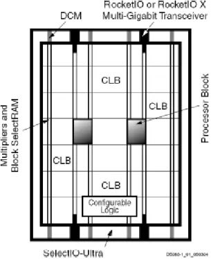
The Virtex II Pro [4] are a family of FPGAs from Xilinx SRAM based technology. As can be seen in Figure 1, shows a nearly symmetrical structure. The CLBs columns are separated, with regular spacing, by a column of BRAMs, with a processor embedded on the left.
Figure 1 - VirtexII Global Architecture
Each CLB consists of four cells divided into two columns, where each column has its own logic of transport as shown in Figure 2 (a). In Figure 2 (b) the logic in each Slice can be observed more closely.
Figure 2 - Structure of a CLB (a) with a detailed view of a slice (b) (based on [6])
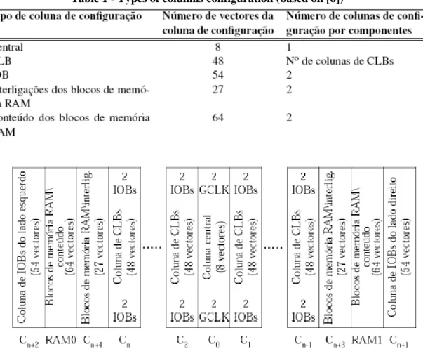
The matrix is organized in vertical channels of a bit of width and length proportional to the number of lines. This is the minimum structure that can be set [5].
Vectors are grouped in columns whose size varies according to Table 1.
Figure 3 shows the allocation of different columns of the memory configuration for configurable resources.
Table 1 - Types of columns configuration (based on [6])
Figure 3 - Organization of memory configuration (based on [6])
The change in memory configuration is done using Bitstream files.
These files contain the configuration of one or more aspects of memory configuration, and may have some parameters associated with the address to which the vector is refered. The Bitstreams are specific to each type of FPGA.
2.3. Operating System
The static optimization of resources is complicated. One more degree of freedom makes the control quite complex. Using an Operating System (OS) to control the resources is an option allowing the natural development of applications with a higher level of abstraction. Despite some loss in performance, increases both the potential flexibility and speed of the project are an added value, representing a good compromise.
With the use of an OS you can develop new applications using known languages, software development, and linking software and hardware in a simple and productive way, optimizing the existing resources.
The OS must support the processes of communication, such as Ethernet or RS232, to manage memory and control peripherals. Thus, designers can focus its attention on the functionality they intend to implement since the OS already recognizes the devices on the system.
The use of known methods eases the adaptation to new systems and architectures allowing a faster adaptation to new users. Thus it is easier to adapt applications already developed for other systems, benefits of the model abstraction making available the OS. This layer of abstraction also allows increasing the portability of new applications.
Because they use the methods provided by the OS, if there is a change in hardware is not necessary to rewrite the application code, just change the driver for that module if necessary. Thus it minimizes the dependence on a specific model of FPGA either during development or after production. [21]
2.4. Linux
The GNU / Linux [7] is an open source OS that supports many target platforms. The PowerPCs embedded in the Xilinx FPGAs are no exception. These processors are supported in kernel versions 2.4 and 2.6. The currently recommended version is the 2.6 and is the one with further development, while in the 2.4 only corrections of bugs was done.
The use of Linux allows the use of "common" tools as compilers and debuggers, enabling new projects to adapt quickly to the new system development. For example, you can run a terminal via serial port, in the FPGA to control the various execution processes.
The Xilinx initiated a project [8] which aims to test and develop code in support of their platforms to GNU / Linux. In the process of testing are drivers for peripherals GPIO, I2C, SPI and USB.
2.5. FPGA utilization trend
Reconfigurable computing is a promising research area that has recently stabilized and nowadays there are plenty of FPGAs with interesting tools at moderate costs making it possible to envisage a small robot with little number of components and hi flexibility that will deliver high performance in a broad spectrum of applications.
In the last decade, it has become aparent that embedded systems are integral parts of our every day lives. The wireless nature of many embedded applications as well as their omnipresence has made the need for security and privacy preserving mechanisms particularly important.
An increasing interest in the design of mobile robots has been observed in recent years, which is mainly motivated by technological advances that may allow their application to consumer markets, in addition to industrial areas. Although sophisticated techniques have been developed, choosing the appropriate hardware-software partitioning and programming robot functions are still very complex tasks. Current approaches often involve the design and implementation of hardwired solutions, with the associated problems of a long development cycle, and little flexibility to deal with changing requirements[22].
FPGAs has gained interest on robotics and mobile robotics applications due to their flexibility to implement from glue logic, up to complete embedded systems for robot control and high level processing. The synergy between robotics and reconfigurable computing is opening new research and application opportunities to build better and more intelligent robots. The special Reconfig track on FPGAs for robotics is aimed to research related to any aspect of Robotics where FPGA and Reconfigurable logic can have an impact. Topics include, but are not limited to[23]:
• Reconfigurable Computing and FPGAs in Mobile Robotics • FPGA based platforms for robotics
• Robot navigation architectures • Robot map creation architectures • Robot protocol and communications
• Bioinspired sensing and controlling architectures implemented on FPGA • Modular robotics
• Robotic control
• Vision processors based on FPGA
Mobile robots have been the central focus of many research works in recent years. Those works have allowed important advances in areas such as algorithms for machine learning and probabilistic models, which can be used to deal with the uncertainty associated with the environment which the robot will interact with, and the data received via sensors.
There are two primary methods in conventional computing for the execution of algorithms. The first is to use hardwired technology, either an ASIC or a group of individual components forming a board-level solution, to perform the operations in hardware. ASICs are designed specifically to perform a given computation, and thus they are very fast and efficient when executing the exact computation for which they were designed. However, the ASIC circuitry cannot be altered after fabrication. This forces a redesign and refabrication of the chip if any part of its circuit requires modification. This is an expensive process, especially when one considers the difficulties in replacing ASICs in a large number of deployed systems. Board-level circuits are also somewhat inflexible, frequently requiring a board redesign and replacement in the event o changes to the application [24].
The second method is to use software - programmed microprocessors / microcontrollers - a far more flexible solution. Processors execute a set of instructions to perform a computation. By changing the software instructions, the functionality of the system is altered without changing the hardware. With the help of the OS, several tasks can be multiprocessed in a manner that only sometimes can be considered simultaneous [24].
However, the downside of this flexibility is that the performance can suffer, if not in clock speed then in work rate, and is far below that of an ASIC. The processor must read each instruction from memory, decode its meaning, and only then execute it. This results in a high execution overhead for each individual operation [24].
Additionally, the set of instructions that may be used by a program is determined at the fabrication time of the processor. Any other operations that are to be implemented must be built out of existing instructions. Reconfigurable computing is intended to fill the gap between hardware and software, achieving potentially much higher performance than software, while maintaining a higher level of flexibility than hardware. Reconfigurable devices, including FPGAs, contain an array of computational elements whose functionality is determined through multiple programmable configuration bits. These elements, sometimes known as logic blocks, are connected using a set of routing resources that are also programmable. In this way, custom digital circuits can be mapped to the reconfigurable hardware by computing the logic functions of the circuit within the logic blocks, and using the configurable routing to connect the blocks together to form the necessary circuit. FPGAs and reconfigurable computing have been shown to accelerate a variety of applications [24].
In order to achieve these performance benefits, yet support a wide range of applications, reconfigurable systems are usually formed with a combination of reconfigurable logic and a general-purpose microprocessor. The processor performs the operations that cannot be done efficiently in the reconfigurable logic, such as data-dependent control and possibly memory accesses, while the computational cores are mapped to the reconfigurable hardware. This reconfigurable logic can be composed of either commercial FPGAs or custom configurable hardware [25].
Compilation environments for reconfigurable hardware range from tools to assist a programmer in performing a hand mapping of a circuit to the hardware, to complete automated systems that take a circuit description in a high-level language to a configuration for a reconfigurable system [25].
The design process involves first partitioning a program into sections to be implemented on hardware, and those which are to be implemented in software on the host processor. The computations destined for the reconfigurable hardware are synthesized into a gate level or register transfer level circuit description [25].
This circuit is mapped onto the logic blocks within the reconfigurable hardware during the technology mapping phase. These mapped blocks are then placed into the specific physical blocks within the hardware, and the pieces of the circuit are connected using the reconfigurable routing. After compilation, the circuit is ready for configuration onto the hardware at run-time. These steps, when performed using an automatic compilation system, require very little effort on the part of the programmer to utilize the reconfigurable hardware. However, performing some or all of these operations by hand can result in a more highly optimized circuit for performance-critical Applications. Since FPGAs must pay an area penalty because of their reconfigurability, device capacity can sometimes be a concern. Systems that are configured only at powerup are able to accelerate only as much of the program as will fit within the programmable structures. Additional areas of a program might be accelerated by reusing the reconfigurable hardware during program execution. This process is known as run-time reconfiguration (RTR). While this style of computing has the benefit of allowing for the acceleration of a greater portion of an application, it also introduces the overhead of configuration, which limits the amount of acceleration possible. Because configuration can take milliseconds or longer, rapid and efficient configuration is a critical issue. Methods such as configuration compression and the partial reuse of already programmed configurations can be used to reduce this overhead [25].
2.6. Applications
Applications of FPGAs include digital signal processing, software-defined radio, aerospace and defense systems, ASIC prototyping, medical imaging, computer vision, speech recognition, cryptography, bioinformatics, computer hardware emulation, radio astronomy and a growing range of other areas [20].
FPGAs originally began as competitors to CPLDs and competed in a similar space, that of glue logic for PCBs. As their size, capabilities, and speed increased, they began to take over larger and larger functions to the state where some are now marketed as full systems on chips (SoC). Particularly with the introduction of dedicated multipliers into FPGA architectures in the late 1990s, applications, which had traditionally been the sole reserve of DSPs, began to incorporate FPGAs instead.[9][10]
FPGAs especially find applications in any area or algorithm that can make use of the massive parallelism offered by their architecture. One such area is code breaking, in particular brute-force attack, of cryptographic algorithms.
FPGAs are increasingly used in conventional high performance computing applications where computational kernels such as FFT or Convolution are performed on the FPGA instead of a microprocessor.
The inherent parallelism of the logic resources on an FPGA allows for considerable computational throughput even at a low MHz clock rates. The flexibility of the FPGA allows for even higher performance by trading off precision and range in the number format for an increased number of parallel arithmetic units. This has driven a new type of processing called reconfigurable computing, where time intensive tasks are offloaded from software to FPGAs.
turn-around times of current design tools, where 4-8 hours wait is necessary after even minor changes to the source code [20].
Traditionally, FPGAs have been reserved for specific vertical applications where the volume of production is small. For these low-volume applications, the premium that companies pay in hardware costs per unit for a programmable chip is more affordable than the development resources spent on creating an ASIC for a low-volume application. Today, new cost and performance dynamics have broadened the range of viable applications [20].
2.7. Tools – Hardware Programming Languages (for FPGAs)
To define the behaviour of the FPGA, the user provides a hardware description language (HDL) or a schematic design. The HDL form might be easier to work with when handling large structures because it's possible to just specify them numerically rather than having to draw every piece by hand. On the other hand, schematic entry can allow for easier visualisation of a design [20].
The most common HDLs are VHDL and Verilog, although in an attempt to reduce the complexity of designing in HDLs, which have been compared to the equivalent of assembly languages, there are moves to raise the abstraction level through the introduction of alternative languages [20].
To simplify the design of complex systems in FPGAs, there exist libraries of predefined complex functions and circuits that have been tested and optimized to speed up the design process. These predefined circuits are commonly called IP cores, and are available from FPGA vendors and third-party IP suppliers (rarely free and typically released under proprietary licenses). Other predefined circuits are available from developer communities such as OpenCores (typically free, and released under the GPL, BSD or similar license), and other sources [20].
3. Robotic Systems and Actuators
3.1. Project Framework
As an application goal, the fire fighting contest was chosen for ease of deployment and because it is now considered somewhat of a standard test for robotics performance. The mentioned contest started in Trintiy College[14] and has also been ported to a low cost but very interesting similar competition at a local level, namely the fire fighting at Instituto Politécnico da Guarda[15].
As refered in the Introduciton chapter the focus of this project is to develop a locomotion system in order to evaluate the future developments of IPs to control full robotic systems.
3.2. Starting Point of the presented work
At the time this work started, some components were alredy chosen and a prototype was somewhat assembled.
Many decisions for the workings of the robot had already been made such as the configuration, sensors and actuators (see figure 28).
The current work will focus on the actuators for the mentioned robot. The complex part of the actuators is, of course, the control of the movement of the robot.
The locomotion system controller will be developed in a wheelchair type robot, mentioned in the chapter 5, with brushless DC (BLDC) motors. For this reason a driver for a brushless DC motor will be the developing focus of this project.
3.3. Requirements analysis
There is no need for any type of advanced drives. It would be interesting to allow the robot maneuver in tight corridors and to be able to turn around himself, due to this requirement a driver with high movement precision is needed. Although interesting, speed is not essential and a maximum of 0.5 m/s is perfectly acceptable.
Identified actuators in the robotic system are:
Geared Electrical Motors – typically DC motor, brushless type
Extinguisher Devices – motor for water sprinkler or fans or hobby servo's
As referred above the focus of the project will be the development of a driver to control the bushless DC motor. The system to develop will control a wheelchair robot type, this means that the development of two drivers is needed.
3.4. Global architecture
FPGA Motor Power Electronic Circuit SuzakuFigure 4 - Locomotion system (Global Overview)
3.5.
Requirements specification
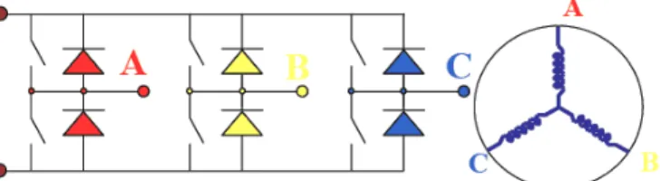
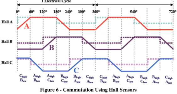
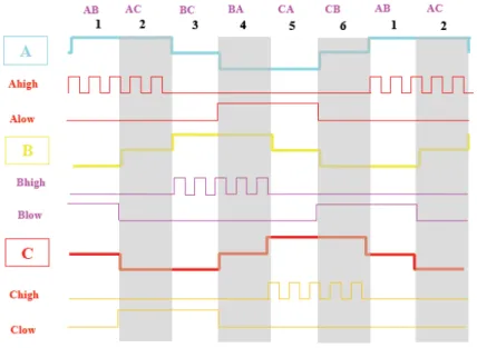
3.5.1. Brushless driver controlThe motor is commutated based on the signals given by the Hall Sensors mounted at various positions inside the motor. Hall outputs change every 60 electrical degrees. The state of the control switches and the Hall sensor signals are scanned continuously. A new voltage vector / control trajectory is applied to the BLDC motor based on the Hall sensor signal conditions. This mechanism is known as commutation.
3.5.2. Sensored Drive – Hall Effect Sensors
The Hall position sensors sense the actual rotor position. The Hall outputs are monitored by the controller and appropriate commutation sequence is applied to assist in commutating the motor. The speed of the motor is varied by making use of PWM outputs on the output voltages. Typically there are three Hall effect sensors provided inside the motor. The three sensors comprise six states: 001, 010, 011, 100, 101, and 110. Six steps are required to perform one complete electrical cycle. The electrical-to-mechanical ratio is based on the pole pairs inside the motor. Each state corresponds to the actual rotor position inside the motor. This determines the required direction of voltage vector based on the direction in which the rotor needs to be moved. A vector table is generated for the sensor state and the next commutation sequence.
Figure 6 - Commutation Using Hall Sensors
3.5.3. Speed Control
The speed of the motor is directly proportional to the applied voltage. By varying the average voltage across the windings, the RPM can be altered. This is achieved by altering the duty cycle of the base PWM signal. Maximum speed is achieved when PWM is OFF. In that case, the MOSFETs are ON for 100% of the commutation period. When PWM is turned ON, the speed is proportional to the duty cycle setting.
3.5.4. BLDC Control State Machine
Figure 8 - BLDC Control State Machine
3.5.5. Control Waveforms
In this case the PWM signal is applied only to the high side of the MOSFET pair, while the low side is driven for 100% of the commutation period.
3.5.6. Brushless Motor
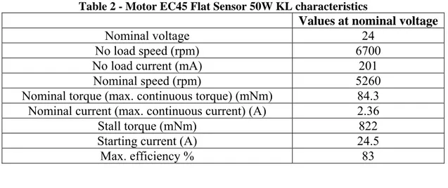
Motor choice is based on power density, efficiency, size restrictions together with gearbox and cost.
The choice was motor EC45 Flat Sensor 50W KL (251601) and gearbox GP 042C (203115), 7.5Nm, 2St, KL. The motor is high power and includes hall sensors and connects integrally to a robust ceramic lightweight planetary gearbox with large stall torque (7 Nm), reduction 12:1.
3.5.6.1. Motor characteristics
Table 2 - Motor EC45 Flat Sensor 50W KL characteristics
Values at nominal voltage
Nominal voltage 24
No load speed (rpm) 6700
No load current (mA) 201
Nominal speed (rpm) 5260
Nominal torque (max. continuous torque) (mNm) 84.3 Nominal current (max. continuous current) (A) 2.36
Stall torque (mNm) 822
Starting current (A) 24.5
Max. efficiency % 83
4. Implementation
4.1. Hardware & Software Design Using Suzaku Board
Recent FPGAs present large “programming” capacities. In order to have large capacity at inexpensive prices, the packaging of these chips is often BGA that are impractical to build in-house PCBs and thus many development boards with FPGAs are available that transform FPGA plus interesting spare electronics into rapid prototyping boards. In this project one of these boards is used.
Figure 10 - Suzaku-V board
The Virtex II Pro is a powerful FPGA + PowerPC in the same chip, implementing a particularly powerful combination of common usage processor (the PowerPC 405) and a FPGA fully available for programming user logic.
The Suzaku-V SZ310-U00 board was chosen to develop the software and hardware applications that will control the robot. The board includes the Virtex II Pro, memory, flash and ethernet on board in a credit card sized board. It is possible to develop dedicated hardware using a HDL (VHDL or Verilog) for the FPGA that communicates with the PowerPC inside the same chip. By using the rich array of IP cores offered by Xilinx and other third parties, it is easy to add required functionality.
The SUZAKU board has 70 free, configurable, I/O pins. From the network protocol stack to the file system, SUZAKU are provided with a proven and stable operating system. The SUZAKU-V makes use of a standard Linux kernel 2.6 releases and uses standard ELF executables.
From device drivers to server applications, it is possible to utilize the wide range of open source Linux compatible software resources. Use of this proven and stable software will shorten development time. The combination of the LAN interface (10BASE-T/100BASE-TX) and Linux's TCP/IP protocol stack makes it easy to develop network ready devices.
Table 3 - Suzaku-V board specifications
SZ310-U00 FPGA Device Xilinx Virtex-II Pro (XC2VP4)
FPGA Clock 3.703 MHz
CPU Core PowerPC405
CPU Clock 265.4208MHz
DRAM SDRAM 32MB
Flash Memory 8MB
Ethernet 10BASE-T/100BASE-TX
User I/O pins 70
Serial Port FPGA intemal 1ch (RS232C) Timer PowerPC internal timer
Configuration TE7720
Dimentions Board Size: 72×47 [mm] Power Supply 3.3V +/- 3% Power Consumption(Typ.) 1.5W Operating Temperatures 0 ~ 60 ° C Supplied Operating System Linux 2.6
The advantages are clear: full speed for the CPU and a full FPGA free to program at the expense of using a slightly higher priced chip. Additional advantages is that full speed communications between FPGA and processor is possible because they are inside the same packaging and external IO pins may be routed though the FPGA as if they were internal to the PPC.
4.2. Tools - Development for the PowerPC under Linux
The Suzaku-V uses a full standard Linux kernel 2.6.xx and as such, device drivers and normal programming tools can be used. Compiled programs can be stored in flash and executed upon boot.
The cross compile tools (to PowerPC) were installed inside a VMWare image in order to shorten installation times for the tool chain.
The Linux development tools are C-Language GCC cross compiler to PowerPC.
4.2.1. Software Development Environment
The software development environment provided with the SUZAKU series boards consists of three tools:
4.2.1.1. ATDE
Figure 11 - (ATDE) Atmark Techno Development Environment
Atmark Techno Development Environment (ATDE) is a VMware virtual machine data image which provides a development environment for the SUZAKU series boards. The image includes a Linux desktop environment along with the GNU cross development tools and other necessary development tools preinstalled. By using ATDE, it is no longer necessary to spend time setting up a development PC and installing the various required tools. ATDE can be used with VMware Player.
4.2.1.2. GNU Cross Development Tools
Kernels and applications to be run on the SUZAKU series boards can be built using the cross compiler and other tools included in the GNU cross development tool chain.
4.2.1.3. Linux-distribution
Product development, involving both application and kernel development, can be carried out using Linux-distribution. Linux-distribution not only provides the ability to customize kernels and make application selections, but can also be used to build image files to be written to the board Flash memory with a single command. With Linux-distribution, it is simple to customize SUZAKU boards in order to produce final products.
4.3. FPGA Development
This project used the standard Xilinx tools: Xilinx Platform Studio, Xilinx ISE, Xilinx EDK and modelSim simulator.
Programming uses netflash and hermitt tools, supplied by Atmark, the Suzaku manufacturers.
Figure 12 - Hardware development top view
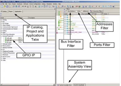
Many Intellectual Property (IP) cores are available for FPGAs that can be connected to these devices, example from Xilinx and from http://www.opencores.org/. These cores offer additional functionalities to the system.
Figure 13 - Tools used for Software & Hardware development
The usage of the software tools has some setup time as there are many types of view for the same system (see Figure 14). Highlights for this interface is the easiness to see the processor buses (Processor local bus – PLB and On-Chip peripheral Bus – OPB) and the catalogue of Intellectual Properties (IPs) that can be added to the system.
4.4. FPGA+ PowerPC Control System Development
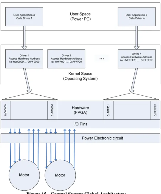
The control system was developed based on the architecture designed on the figure 15.
The system was distributed by the low and high level layers. The main property of the applications developed in the high level layer is the high calculation capacity but less actuation speed when compared to the applications developed in the low level layer. The control applications were distributed by these layers based on the properties above mentioned.
In the following figure the high and the low level layers are respectively referred as the User Space and the FPGA area.
Figure 15 - Control System Global Architecture
In the high level the goal is to develop a control/decision application in the PowerPC capable of communicate with the FPGA IP cores.
The long term goal of this project is to develop IPs, in the low level layer, with the capacity to control the full robotic system, this means IPs capable of controlling actuators like DC motors, servos and motors for water sprinkler.
Figure 16 - Global Architecture with - IPs to full robotic control system
As refered in the sub-chapter 3.1 the focus of this project is to develop a IP core capable of controlling a brushless Motor.
From the PowerPC application the user only sends the reference velocity to the Brushless driver IP core. The velocity control loop is implemented in the FPGA hardware due to the main property of the applications developed in these layers that is the high actuation speed (see figure 18). Future work will include receiving [velocity and angular velocity] and driving together a pair of BLDC motors.
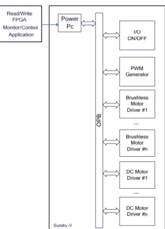
OP B Suzaku-V Brushless Motor Driver #1 Target Velocity (rpm) Power Pc
Velocity
Control Loop
Brushless Motor Driver #2Velocity
Control Loop
Figure 18 - Brushless Driver IP – Velocity control loop
For the communication between PowerPC application and the FPGA IP core a Linux Device Driver development is needed.
4.5. Hardware/IP Development in the FPGA
The goal of the IP developed in the FPGA is to drive a brushless motor.
This IP is able to read the digital signal generated by the hall sensors available in the brushless motor and based on the number of impulses the IP is capable to estimate the motor velocity and keep it in a register that will be accessible from the PowerPC.
The PID block implemented in the IP guarantee that the motor runs at the reference velocity sent by the PowerPC application.
The FPGA signal level is 3.3V and is quite vulnerable to problems in the power circuit. For safety, voltage adaptation, current adaptation and isolation purposes, the TLP2630 optocoupler is used.
4.5.1. IP Block Diagram – Global View
The IP was developed using the XPS toll. Xilinx Platform Studio (XPS) is an integrated tool for specifying and building both hardware and software embedded development. The FPGA hardware was designed using this tool as an interface to the Xilinx ISE tool. The embedded processor part of the system design will be completed and added to the IP by this tool during the compilation process.
Figure 19 - Brushless Motor Driver IP – Global overview
The PowerPC communicates with the IP developed through the OPB.
The IP is developed in two parts, the first part it’s implemented in the driver.vhd and the second one in the user_locig.vhd file.
The interface between the OPB and the IP registers is configured in the driver.vhd, this is the main part of the IP.
The registers as well as the custom logic to make the IP working as the user wants will be defined in the user_locig.vhd file. This part is instantiated by the first file.
The connection between the registers and the physical Input and Output ports of the Suzaku-V board will be established in the .ucf file.
4.5.2. IP Block Diagram – Detailed view 4 Velocity estimator 3 Duty calculator 5 “Encoder” Motor registers Phase A Phase B Phase C Hall C Hall B Hall A Estimate Rpm (rpm_estimate) PWM duty (pwm_length)
Hall Amostrage Timer (timer_hall_a) registers 2 Phase Switch 1 Wave Form generator PWM signal (pwm) registers Increment phase ( inc_phase) Hall State (hall_state) Boot Signal (vboot)
PowerPC bus Values for register 1 3 4 Power
PC
Brushless Control IP
OPB <–> IP interface
Figure 20 - Brushless Motor Driver IP – detailed view
All the clocks are synchronized with the main clock of the IP core that has a frequency of 3,7Mhz.
4.5.2.1. IP Block diagram description
During the initialization the registers of some blocks are configured.
The PWM control frequency, the hall signals sensors sample frequency as well as other values, that will be explained later, are calculated in the user-space application (PowerPc) and sent to the FPGA registers during the initialization.
The Initialized registers are:
timer_hall_rf <= conv_integer(slv_reg0); -- block 1 dtk <= conv_integer(slv_reg1); -- block 4 dtime <= conv_integer(slv_reg2); -- block 1 inc_phase <= conv_integer(slv_reg3); -- block 3 pwm_max <= conv_integer(slv_reg5); -- block 1 rpm_ref <= conv_integer(slv_reg8); -- block 3 inc_pwm <= conv_integer(slv_reg9); -- block 3
Rpm_ref defines the register were the target velocity is stored.
Timer_hall_rf defines the sample control frequency by configuring the maximum value of the counter that will implement the hall signals sensors sample time.
Pwm_max defines the PWM control frequency by configuring the maximum value of the counter that will implement the PWM control signal.
dtk is a constant that allows to calculate the velocity in rpm based on the number of impulses redden during the hall signal sensors sample time. The calculation of this value will be explained in the block 4 description.
Inc_pwm it’s the registers that defines the number of PWM control steps increment. Inc_phase will be explained in the block 3 description.
Block 1:
In this block the PWM waveform, the clock that defines the sample frequency of the hall sensors signals as well as the boot signal for the electronic power circuit are generated.
Figure 21 - Gene ted Waveforms
o generate multiple signals with different frequencies based and synchronized with the
ra
T
main clock, multiple counters were implemented. The counter values are calculated based on the following equation:
Main_clock_frequency Counter_Value=
Target_frequency impulses per revolution of the motor is 48.
ollowing equation: The number of
The number of counted impulses is calculated based on the f Velocity(rpm)
Counted_Impluses= *Impulses_per_revolution*sample_time 60
The hall signal sensors sample time was defined based on the velocity sample resolution that was chosen to be 50rpm. (the number of impulses counted during the sample time for the minimum velocity should be 1):
50
1= *48*sample_time sample_time=25ms sample_frequency=40hz
60
3,7Mhz
Sample_Timer_Counter_Value= =92500 40hz
following equation: The PWM control resolution is calculated based on the
Maximum_velocity PWM_control_resolution=
The PWM control resolution should higher or equal to the velocity sample resolution: 6700rpm 50 Number_of_PWM_steps 134 Number_of_PWM_steps PWM_Timer_Counter_Value=134 _ _ 3,7 PWM_frequency_control= 27, 4 _ _ _ 134
Main clock freqeuncy Mhz
Khz
number of control steps
The frequency of the Vboot signal is 44us, this signal is used to generate a voltage higher than VGS on VDS and ensure that the MOSFET is always driving because as an N channel MOSFET VDS is approximately 0v and Vcc approximately Vs and so the MOSFET on the superior part of the H-Bridge would not work properly because VGS would also be 0v. VHDL code: process(clk) begin if (rising_edge(clk)) then if ( count_vboot > 540 ) then
if ( count_vboot > 2880 ) then count_vboot<=0;
else count_vboot <= count_vboot+1;
end if; vboot <= '0'; else vboot <= '1'; count_vboot <= count_vboot+1; end if;
if ( timer_pwm > pwm_length ) then
if ( timer_pwm > pwm_max ) then timer_pwm<=0;
else timer_pwm <= timer_pwm+1;
end if;
pwm<="0000";
else
if ( timer_pwm < dtime ) then pwm<="0000";
else pwm<="0111"; end if; timer_pwm <= timer_pwm+1; end if; if(timer_hall_a>=timer_hall_rf) then timer_hall_a<=0; else
Block 2:
In this block the control signal to each phase of the motor is achieved based on the hall sensors signal state.
VHDL code: process(clk,inc_phase,hall_state) is begin if (rising_edge(clk)) then hall_state_mi<=hall_state+inc_phase_a; end if; end process; process(clk,timer_pwm,hall_state_mi) is begin
if (rising_edge(clk)) and (timer_pwm=0) then if(conv_integer(rpm_ref)>0) then
case hall_state_mi is
when 1 => phase_select<="0100"; hiz<="010"; -->I-II when 2 => phase_select<="0010"; hiz<="100"; -->II-III when 3 => phase_select<="0010"; hiz<="001"; -->III-IV when 4 => phase_select<="0001"; hiz<="010"; -->IV-V when 5 => phase_select<="0001"; hiz<="100"; -->V-VI when 6 => phase_select<="0100"; hiz<="001"; -->VI-I when others => phase_select<="0000"; hiz<="000"; end case;
else
case hall_state_mi is
when 1 => phase_select<="0100"; hiz<="001"; -->I-VI when 2 => phase_select<="0100"; hiz<="010"; -->II-I when 3 => phase_select<="0010"; hiz<="100"; -->III-II when 4 => phase_select<="0010"; hiz<="001"; -->IV-III when 5 => phase_select<="0001"; hiz<="010"; -->V-IV when 6 => phase_select<="0001"; hiz<="100"; -->VI-V when others => phase_select<="0000"; hiz<="000"; end case;
end if;
phase <= (phase_select and pwm); end if;
Block 3:
In this block the duty cycle of the PWM control signal is achieved based on the estimated velocity calculated on the block 4. The increment of the duty cycle value is ruled by the register inc_pwm, configured during the initialization of the IP.
This increment is applied to the pwm_length_init register that is calculated by the PowerPC application in order to improve the time driver response.
Due to mechanical clearences sometimes the hall sensors signals does not correspond to the correct state of the motor and it stops because the phase signal and hall sensors signal are not synchronized. In order to avoid this problem an increment on the phase control signal is done if the target velocity is not zero and if the estimated velocity is zero from more than 5 cycles. This increment is ruled by the register inc_phase, configured during the initialization of the IP.
VHDL code:
--- CODE TO ESTIMATE THE PWM LENGTH PULSE --- process(clk,rpm_estimate,timer_hall_a) is begin if (rising_edge(clk)) then if (timer_hall_a=0) then if(abs(rpm_estimate)<abs(rpm_ref)) then pwm_length_e<=(pwm_length_e+inc_pwm); end if; if(abs(rpm_estimate)>abs(rpm_ref)) then pwm_length_e<=(pwm_length_e-inc_pwm); end if; if(rpm_estimate=0) then rpm_count<=rpm_count+1; else rpm_count<=0; end if; else pwm_length_e<=pwm_length; end if; end if; end process; process(clk,pwm_length_e) is begin if (rising_edge(clk)) then if(pwm_length_e>pwm_max) then pwm_length<=pwm_max; else if(pwm_length_e<0) then pwm_length<=0; else pwm_length<=pwm_length_e; end if; end if;
process(clk,rpm_count) is begin if (rising_edge(clk)) then if(rpm_count>5) then if(conv_integer(rpm_ref)>0) then inc_phase_a<=inc_phase; else inc_phase_a<=- inc_phase; end if; else inc_phase_a<=0; end if; end if; end process;
Block 4:
In this block the velocity of motor is calculated based on the number of impulses counted during the sample time:
Velocity(rpm) Counted_Impluses= *Impulses_per_revolution*sample_time 60 60*Counted_Impluses Velocity(rpm)= Impulses_per_revolution*sample_time
dtk is a register that allows to estimate the velocity in rpm:
60*Counted_Impluses Velocity(rpm)= =Counted_Impluses*dtk Impulses_per_revolution*sample_time dtk= 60 = 60 =50 Impulses_per_revolution*sample_time 48*25ms VHDL code: process(clk,timer_hall_a) is begin if (rising_edge(clk)) then hall_state_mb<=hall_state; if (timer_hall_a=0) then count_hall_mb<=count_hall_m; rpm_estimate<=(conv_integer(count_hall_m))*dtk; count_hall<="00000000000000000000000000000000"; else count_hall_m<=count_hall; if (hall_state > hall_state_mb) then
if (hall_state = 6 and hall_state_mb =1) then count_hall<=count_hall-1;
else
count_hall<=count_hall+1;
end if;
end if;
if (hall_state < hall_state_mb) then
if (hall_state =1 and hall_state_mb = 6) then count_hall<=count_hall+1; else count_hall<=count_hall-1; end if; end if; end if;
Block 5:
In this block the state of the motor is achieved based on the state of the hall sensors signal.
VHDL code:
process(hall) is begin
case hall is
when "101" => hall_state<= 1;-->I when "100" => hall_state<= 2;-->II when "110" => hall_state<= 3;-->III when "010" => hall_state<= 4;-->IV when "011" => hall_state<= 5;-->V when "001" => hall_state<= 6;-->VI
when others => hall_state<= hall_states; end case;
4.6.
Device Driver development
The user application developed in the PowerPC is able to access (read/write) the IP registers implemented in the FPGA.
Figure 22 - FPGA(IP) architecture
In order to communicate with the FPGA IP a Linux Character Device Driver was developed to access the address in witch the FPGA registers data is stored.
Table 4 - Suzaku-V 310 memory map
The Address in witch the FPGA registers data is stored is defined in the ISE project. This address select to implement the registers could be placed in any free memory address.
There are two ways of compiling a device driver: statically built into the kernel or as a module.
Modules have the advantage that they can be loaded and unloaded during runtime. Therefore, during development it becomes necessary to compile the device driver as module.
The development of a device driver as a module was not possible due to some compilations errors that can not be solved, for this reason a static device driver was developed.
4.6.1. Steps to develop a static device driver
User Space (Power PC)
driver.c
Access Hardware Address 0xF0FD200 … 0xF0FD3FF
User Application uses driver.c compiled on the
Kernel space
Hardware (FPGA)
Kernel Space
Kernel node: /dev/fpga
Figure 23 - Access FPGA hardware trough character device driver
4.6.1.1.Generating the kernel node
Char devices are accessed through names in the file system. Those names are called special files or device files or simply nodes of the file system tree[12].
Open the following directory:
/home/Desktop/atmark-dist-20080314/vendors/AtmarkTechno/SUZAKU-V.SZ310SIL
Open the Makefile and add the following line after the last DEVICE statement and before the FLASH_DEVICES statement:
“DEVICE += fpga,c,250,0”
4.6.1.2. Generating the module
This module will be used by the user-space application, to generate it it’s necessary to generate a new sub-directory called driver in the following directory:
/home/Desktop/atmark-dist-20080314/linux-2.6.x/drivers/char Add the following lines to the Makefile of the following directory:
/home/Desktop/atmark-dist-20080314/linux-2.6.x/drivers/MakeFile subdir-m += driver
obj-m += driver/driver.o
On the new directory add the file with the functions that will be used by the user-space application(s).
In this example the file it will called as driver.c. The functions used by the user-space applications are[11]:
fpga_read(struct file *filp, char *buf, size_t count, loff_t *f_pos) used to read values from FPGA registers
fpga_write(struct file *filp, unsigned char *buf, size_t count, loff_t *f_pos) used to write values to FPGA registers
fpga_init(void) – used to open the device driver fpga_exit(void) – used to close the device driver
This files (driver.c and Makefile) are attached in the Appendix B. driver.c:
int fpga_major = 250;
#define FPGA_BASE 0xF0FD200 Change this addresses to access the desired FPGA ZONE Check on the XPS project the addresses
#define FPGA_MAX 0x F0FD3FF static void *io_base;
ssize_t fpga_read(struct file *filp, char *buf, size_t count, loff_t *f_pos) {
… }
ssize_t fpga_write(struct file *filp, unsigned char *buf, size_t count, loff_t *f_pos) {
read: fpga_read, write: fpga_write, poll: NULL, open: NULL, release: NULL, };
static int fpga_init(void) {
… }
static void fpga_exit(void) { … } module_init(fpga_init); module_exit(fpga_exit); MakeFile: EXTRA_CFLAGS += -I$(TOPDIR)/arch/ppc/platforms/xilinx_ocp list-multi := driver.o
# The Linux adapter for the Xilinx driver code. driver-objs += driver.o # The Xilinx OS independent code.
driver-objs += driver.c obj-$(CONFIG_REG_DRIVER) := driver.o
driver.o: $(driver-objs)
$(LD) -r -o $@ $driver-objs)
4.6.1.3. Compiling the Kernel
Now that a new module with the functions that will be used by the user application(s) was added to the Linux Kernel, a compilation is needed in order to generate the .bin file that will be later transferred to the FPGA.
Execute the make command on the following directory to compile the kernel:
/home/Desktop/atmark-dist-20080314 The result will be the image.bin file placed on the following directory:
/home/Desktop/atmark-dist-20080314/images
4.6.2. Transfer the Kernel image to the Suzaku-V board
Open the following directory and transfer the image.bin file to a server directory: /home/Desktop/atmark-dist-20080314/images
Open a telnet session on the Suzaku-V board (User:root Password:root): telnet IP_from_the_Suzaku-v_board
(i.e: telnet 192.168.1.33) Execute the following netflash command:
netflash -ukiH -r /dev/flash/image http://server/image.bin (i.e: netflash -ukiH -r /dev/flash/image http:// 192.168.1.34/image.bin)
4.6.3. Device Driver Testing
Introduce the LED address in the device driver ( 0x0F0FA200 - 0x0F0FA3FF ), on the driver.c file change the following lines:
#define FPGA_BASE 0xF0FA200 Change this addresses to access the desired FPGA ZONE Check on the XPS project the addresses
#define FPGA_MAX 0x F0FA3FF
Compile the new image and send it to the FPGA. Open a telnet session on the FPGA and insert the module executing the following command:
insmod lib/modules/2.6.18-at2/kernel/drivers/char/driver/driver.ko execute echo –n FFFFFF > /dev/fpga and the LED should turn-off
Figure 24 - Testing the device driver – Led OFF
execute echo –n FFFF00 > /dev/fpga and the LED should turn-on
4.7.
PowerPC Control Application
This application was developed in C language supported by the Atmark Techno Development Environment.
The application code is attatched in the Appendix B.
The main task of this application is to send the target velocity to the IP. The initialization values of the IP registers, mentioned on the sub-chapter 4.5.2.1, is done using the functions located in the static device driver developed:
fpga_write(handlemem, &vel_amostrage, 4, 0); fpga_write(handlemem, &dtk, 4, 1*4); fpga_write(handlemem, &dtime, 4, 2*4); fpga_write(handlemem, &inc_phase, 4, 3*4); fpga_write(handlemem, &pwm_max, 4, 5*4); fpga_write(handlemem, &timer_hall, 4, 7*4); fpga_write(handlemem, &ref, 4, 8*4); fpga_write(handlemem, &inc, 4, 9*4);
handlemem is a file handler descriptor associated to the kernel node “linked” to the
developed static driver.
#define FPGADEVICE "/dev/fpga" handlemem = open(FPGADEVICE,O_RDWR);
4.8. Power Electronic Circuit
The power electronic circuit was developed based on the electronic driver developed by the 5DPO department to control a DC motor.
Changes were done to the electronic driver, only the power electronic circuit was used. A new arm was added to the H-Bridge since the electronic driver was only ready to drive an H-Bridge with two arms (blue bounded in Figure 27).
The embedded control circuit on this driver (red bounded in Figure 27) was removed, because it is now implemented in the FPGA, input and output ports were reworked in order to match the interface specifications of the new control circuit. The alimentation circuit (yellow bounded in Figure 27) was also adapted to the new specifications.
Figure 27 - 5DPO DC motor driver - PCB
By the time that this thesis is being written the new PCB with the changes mentioned above have not yet been completed, but the layout and schematic of the electronic circuit is attached in Appendix C.
5. Validation platform and Results
The system developed in the Suzaku board it was tested and verified in a robot based on an FPGA chip developed for the SoftCore robot project.
5.1. SoftCore Robot
The goal of this project is to set the way for a robot with minimalistic component and pin count. This is expected to allow for a small in size but very powerful and versatile robot. The processing is to be based on an FPGA+Microprocessor in the same chip.
The proposed example application is the Fire Fighting contest at Instituto Politécnico da Guarda
5.2. Verification/Validation
The verification and validation of this project was supported by a graphical interface tool develop in Delphi.
Figure 29 - Graphical interface tool
This application is used to send the target velocity to the IP as well to read the velocity and the PWM duty cycle value.
This application stores this data in a file that can be later used to analyze the driver behaviour.
With some small changes this interface can be used to initialize the IP registers mentioned on the 4.5.2.1 sub-chapter.
5.2.1. Delphi- PowerPC Communication Protocol
The communication between the PowerPC application and the Delphi interface is supported a communication protocol developed with the following architecture:
PC (Windows – Delphi) FPGA RS232 BGxxxxAyyyBED
B G x x x x A y y y B E D xxxx -> measured velocity ( 0 to maximum velocity (6700 rpm)) yyy -> number PWM steps ( 0 to maximum number of PWM steps (670)) Each DataStream contains information related to the measured velocity and number of PWM steps applied to the motor.
5.3. Results
In this chapter the response time and resolution of the driver will be analyzed. Linearity, regarding control signal and the response of the driver, will also be analyzed.
The data was collected with the motor running with no load.
5.3.1. Driver Response – no transitory regime
To analyze the driver response and driver resolution, steps of 100 rpm starting on 1000 rpm and finishing on 6000 rpm were applied to the system. The steps increments were only applied after the velocity stabilization.
Reference vs Measured Velocity
y = 0,9985x + 6,4514 0 1000 2000 3000 4000 5000 6000 0 1000 2000 3000 4000 5000 6000 Reference velocity (rpm) Measur e d Velocity (r pm)
Graphic 2 - Driver response - no transitory regime
From the data analyses it’s possible to conclude that driver is capable of reaching the target velocity.
5.3.2. Error analysis
Velocity Error -100 -50 0 50 100 0 50 100 150 200 Sample number E rro r ( rp mGraphic 3 - Driver error analysis
The maximum absolute error, after velocity stabilization, it’s 50 rpm which matches the initial driver specifications.
5.3.3. Time response analysis
In this sub-chapter the driver performance in transitory regime will be analyzed. A step of 3000 rpm was applied in order to evaluate the control system time response.
Time response 0 500 1000 1500 2000 2500 3000 3500 0 1 2 3 4 5 6 7 8 9 10 11 12 13 14 15 16 17 18 19 20 Time(s) M e as u red V el o c it y ( r
Due to the PWM duty cycle estimation block the system response to the input velocity it’s virtually instantaneous, and the time it takes to reach the target velocity is the time needed to set the "thin" adjust implemented in the developed IP (block 3).
5.3.4. Velocity vs PWM control signal – Linearity analysis
PWM vs Measured velocity y = 63,552x - 163,56 0 1000 2000 3000 4000 5000 6000 7000 0 20 40 60 80 100 PWM Duty Cycle (%) Measured V e lo ci ty (rpm )
Graphic 5 - Linearity analysis
The collected data allows to conclude that there is a linearity relation between the system response the PWM control signal.