Article
J. Braz. Chem. Soc., Vol. 25, No. 3, 526-531, 2014. Printed in Brazil - ©2014 Sociedade Brasileira de Química 0103 - 5053 $6.00+0.00
A
*e-mail: [email protected]
Optical Properties and Surface Morphology of ZnTe Thin films Prepared by
Multiple Potential Steps
Murilo F. Gromboni,Francisco W. S. Lucas and Lucia H. Mascaro*
Laboratório de Eletroquímica e Cerâmica (LIEC), Departamento de Química, Universidade de Federal de São Carlos, Rod. Washington Luis, km 235, 13565-905 São Carlos-SP, Brazil
Nesse trabalho foram obtidos eletrodepósitos de filmes finos de ZnTe sobre substrato de Pt, usando pulsos potenciotásticos. A influência do número de pulsos, tempo de deposição para cada elemento (Zn ou Te) e a ordem de deposição das camadas (Zn/Te ou Te/Zn) na morfologia, propriedades ópticas e na foto-corrente foi avaliada. Os dados de microanálise mostraram que a razão Zn/Te variou entre 0,12 e 0,30 sendo que o filme não era estequiométrico. Entretanto, o valor de energia da banda proibida obtido, em todas as condições experimentais utilizadas neste trabalho, foi de 2,28 eV, indicando a formação do filme de ZnTe. As amsotras com maior porcentagem de Zn apresentaram maior fotocorrente, a qual foi da ordem de 2,64 µA cm–2 e uma
morfologia do tipo dendrítica.
In this work, the ZnTe thin films were electrodeposited using potentiostatic steps, on Pt substrate. The effect of steps number, the deposition time for each element (Zn or Te) and layer order (Zn/Te or Te/Zn) in the morphology, composition, band gap energy and photocurrent was evaluated. Microanalysis data showed that the ratio Zn/Te ranged from 0.12 and 0.30 and the film was not stoichiometric. However, the band-gap value obtained from in all experimental conditions used in this work was 2.28 eV, indicating film growth of ZnTe. The samples with higher Zn showed higher photocurrent, which was of the order of 2.64 µA cm–2 and dendritic morphology.
Keywords: electrodeposition, semiconductor, photocurrent, ZnTe thin film
Introduction
Current studies show that Zinc-based II-VI compound semiconductors (e.g., ZnO, ZnTe and ZnSe) have large band gap energy.1-4 Zn-X semiconductors can be applied
to optoelectronic devices such as light emission diodes and photovoltaic solar cells.5 ZnTe is one of the type II-VI
semiconductors that present good optical properties. It shows a direct optical band gap of 2.2-2.3 eV at room temperature, low resistivity and high transparency in the visible spectral domain. Because of these excellent characteristics, ZnTe thin films are used widely in modern solid-state devices, including photovoltaic and solar cells, green light emission and thermoelectric devices and photodetectors.6-10. Thin films
of ZnTe can be obtained by different physical and chemical techniques both at room and at high temperature and it is found as a polycrystalline material in nature. The more usual techniques used to prepare polycrystalline thin films of ZnTe are thermal evaporation,11 sputtering,12 chemical
vapour deposition13 and electrodeposition.14-16 Among
these techniques, electrodeposition is the most suitable method because it is low cost and it allows the coating of large areas with good lateral control of the material quality. Mahalingam et al.17 studied the potentiostatic electrodeposition
of ZnTe thin films on indium-doped tin oxide coated glass (ITO) substrates from an aqueous solution. They observed the ZnTe using scanning electron microscopy (SEM) images and found that nanowires protruding from nanorods had grown, which presented a direct transition band gap energy estimated at about 2.26 eV. Secondly, the authors established that the ZnTe-nanostructured grains with high surface-to-volume ratios could be applied in the construction of high-efficiency gas sensors. A similar system was evaluated by Diso et al.;18
however, in this case, the bandgap of the polycrystalline ZnTe layers was in the range of 2.65-2.75 eV for the ZnSO4
precursor and 2.70-2.87 eV for the ZnCl2 precursor; this increase was attributed to the quantum effect.
acid (9-AnCOOH). Compared with the unmodified TiO2
NT, the ZnTe modified TiO2 NT showed significantly
enhanced photocatalytic activity under simulated solar light. The increased efficiency of photodegradation was due mainly to the improved photocurrent density, which resulted from the enhanced visible-light absorption and decreased hole-electron recombination due to the presence of the p-type semiconductor ZnTe.19 The influence of the
Zn(II) concentration in solution was investigated in the ZnTe’s electrodeposition from solution containing citric acid and sodium citrate. The dependence of the structure, composition and surface morphology was evaluated. The results demonstrated that as the Zn concentration in the electrolyte was reduced, the resistivity of the films obtained decreased continuously and that their band gap increased.20
Another paper reported the ZnTe electrodeposition process from a highly acidic aqueous sulfate electrolyte and discussed the relationships between the electrochemical kinetics and the crystalline structure of the electrodeposits. It was observed that the nucleation process is instantaneous and that the films had a cubic crystalline structure.15 ZnTe
nanowires on the anodic alumina membrane (AAM) membranes with 50-nm pore diameters were prepared through potentiostatic electrodeposition conditions. The electrodeposited ZnTe nanowires were characterised by SEM and X-ray diffraction analysis. The latter showed that they presented a preferential crystalline growth along the crystalline plan (200), which is different to that reported in the scarce literature available on this subject.21
The literature review shows that there is a very sensitive and complex dependence of film microstructure on the preparation method and deposition conditions. Thus, it is important that studies seek to establish the deposition conditions that produce ZnTe films that have a particular crystalline structure with the desired optical properties and morphology. This paper studied the multiple steps in the potentiostatic electrodeposition of ZnTe thin films from aqueous solution on Pt substrates. The effect of the steps numbers, the deposition time for each element (Zn or Te) and the layer order (Zn/Te or Te/Zn) on the morphology, composition, band gap energy and photocurrent response was evaluated.
Experimental
The reagents used were 99.9% TeO2 , ZnSO4.7H2O
and H2SO4 from Sigma Aldrich. Aqueous solutions were
prepared with deionized water taken from a GEHAKA purification system. For the electrodeposition of films, a solution was prepared with 100 mmol L–1 ZnSO
4 and
1 mmol L–1 TeO
2 in 0.5 mol L–1 H2SO4, pH 0.30. The
photoelectrochemical experiments used a 0.1 mol L–1
ferrocene ([Fe(C5H5)2]) in acetate nitrile (C2H3N) and
0.5 mol L–1 sodium perchlorate (NaClO 4).
Electrochemical measurements were performed using an Autolab® PGSTAT 302N potentiostat system with
Autolab GPES software. The electrodes used were a platinum wire counter electrode and a potassium chloride saturated silver (Ag/AgCl/KCl(sat)) reference electrode. The
working electrodes were Pt polycrystalline plates with a geometrical area of 0.9 cm2. The photocurrent system was
a xenon lamp (150 W) from Newport 66902 and the cell that was used in this experiment had a quartz window and 3-cm optical distance. The temperature during all experiments was maintained at 25 °C using a thermostatic bath of Polystat® from Cole-Parmer.
The films were obtained by multiple potentiostatic steps at –0.2 and –0.7 V, where the potentials were choose from cyclic voltammetric results and are related to Te and Zn deposition, respectively. To assess the influence of the species deposited initially on the substrate (Zn or Te) and of the thickness of each layer on the optical properties of the films, several samples were prepared under the conditions given in Table 1. The total polarisation time was 35 min, which was the same for all the prepared samples; the initial polarisation potential (–0.2 or –0.7 V) and the number of steps for the deposition of each (12, 30, 120 and 300 s) was varied. The time change for each step allowed the modification of the thickness of each layer and also of the number of layers. The variation of initial polarisation potential enabled the selection of whether the first layer deposited was Zn or Te.
T h e p h o t o c u r r e n t w a s a n a l y s e d u s i n g t h e chronoamperometric technique at light on and off, applying 0.2 V more positive than the open circuit potential for 300 s with the chopper period adjusted to 50 s. SEM images and energy dispersive X-ray spectroscopy (EDS) spectra were obtained using a microscope mod 35 VP Zeiss-Supra. Reflectance UV-Vis spectra were obtained using a UV-VIS
Table 1. Experimental conditions for the preparation of ZnTe thin films by potential steps
Sample E1dep / V t1 / s E2dep / V t2 / s
Number of cycles Te/Zn
120/300 –0.2 120 –0.5 V 300 5
300/120 –0.2 300 –0.5 V 120 5
30/12 –0.2 30 –0.5 V 12 50
Zn/Te
120/300 –0.5 120 –0.2 300 5
300/120 –0.5 300 –0.2 120 5
HITACHI U-3900H spectrometer. The band gaps of the films were calculated from transmission studies carried out to investigate the optical absorption properties of the ZnTe films; the optical band gap should obey the following Tauc equation, from the plot of (ahν)2vs. photon energy (hν).22
(ahν)2 = cte (hν- Eg) (1)
where α is the absorbance, h is Planck constant and ν the
frequency. Plotting (hν)2vs. hν we can determine the band
gap (Eg ).
Results and Discussion
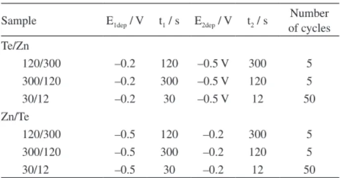
Initially, the voltammetric behaviour of the Te(IV), Zn(II) and Zn(II) + Te(IV) solutions were analysed using a Pt substrate. The objective was to determine the potentials of the deposition and dissolution of each species, which were used to grow the films. Figure 1 presents the cyclic voltammograms obtained from the individual and the mixture of the ionic species at 0.5 mol L–1 H
2SO4, pH 0.30.
It can be observed in the cathodic sweep (green curve, Te) that there is one peak at 0.55 V, which is characteristic of the reduction of Te(IV) to Te0. There are two peaks in the
anodic branch at 0.55 and 0.65 V, which can be related to the dissolution of the deposited Te and the bulk and of underpotential conditions.23,24In the case of Zn (red curve)
a cathodic peak is visible at –0.7 V, corresponding to the reduction of Zn(II) to Zn0 and another very low anodic
peak at –0.35 V, which is due to the dissolution of the Zn coating. The observed Zn dissolution current is low because Zn deposition occurs simultaneously with the hydrogen evolution reaction (HER) and because the HER has a cathodic current, the total anodic current observed on the voltammogram is reduced. This behaviour is usually observed for metal ions that are reduced at very negative potentials.9 In addition, the crossing of the cathodic and
anodic currents is observed in the Zn voltammograms when the direction of sweep is changed, which is indicative of the nucleation of the metallic phases.25
For the mixture of ions, the peak at –0.7 V attributed to Zn deposition is no longer observed. In this case, the cathodic current increases exponentially due to the HER. However, a well-defined anodic peak appears at +0.52 V which presents a higher dissolution charge and more negative peak potential compared to pure Te. This behavior is typically associated with the formation of a new phase in voltammetry dissolution alloys.26 Therefore, we can say that this peak is not related
to pure Te dissolution process, but probably a ZnTe phase, which is formed during the cathodic sweep by co-deposition of Te and Zn. From cyclic voltammograms were chosen for
potential deposition of the layers, which were –0.7 V for Zn and –0.2 V for Te deposition.
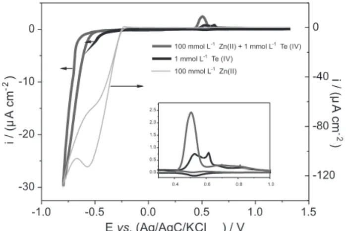
Several samples of ZnTe films were prepared under the conditions described in Table 1, which were analysed by SEM. The micrographs of some samples are shown in Figure 2. These micrographs relate to the Zn/Te and Te/Zn films with different thickness for each layer, as described in the experimental section.
It can be seen from Figure 2 that the films are uniform, dense and strongly adherent to the substrates and that they present two different types of morphology. One is formed by small globular crystals and the other is a dendritic structure with uniform branches. The branches have different thicknesses and they have an arrangement parallel to the substrate. The samples have examples of both morphologies but one type is usually dominant. The morphology type seems more influenced by the deposition time of each metal ion than by the order of the growth of the layers (Zn/Te or Te/Zn).
The samples obtained under the conditions when the polarisation time is long (120 and 300 s), corresponding to five cycles of deposition, are shown in Figure 2a, 2b, 2d and 2e. In this case, irrespective of whether the deposition is Zn/Te or Te/Zn at –0.7 V, when Zn deposition or ZnTe co-deposition occurs at 300 s (Figure 2a and 2e), the film morphology is dendritic and the branches are thick. However, when the deposition time is 300 s at –0.2 V (Figure 2b and 2d), for Te(IV) reduction, the coatings are constituted by thin wire dendrites and some globular crystals. Therefore, we can conclude that the dendritic morphology is associated with species deposited at –0.7 V, i.e., Zn or ZnTe deposition. Comparing the samples obtained at 50 cycles, where the polarisation time at each potential is 10 times lower than for the previous samples
Figure 1. Cyclic voltammograms for Pt electrodes in 1 mmol L–1 Te(IV),
100 mmol L–1 Zn(II) and 100 mmol L–1 Zn(II) + 1 mmol L–1 Te(IV)
0.5 mol L–1 H
(Figure 2c and 2f), the morphology of the Zn/Te or Te/Zn is very similar and presents two structural forms, independently at –0.7 or –0.2 V when the deposition time is high. These coatings seem thinner and do not cover the substrate surface completely.
The dendritic branches were analysed with the aid of Image’J software and the thicknesses of these structures were calculated to vary between 10 and 200 nm. The nanosizes of these structures are good because they provide a high surface area for the material, which is beneficial for applications in photo-sensible devices. By increasing the polarisation time at –0.7 V, these will be the preferential structures once the preformed nanowires have lower energy and will act as nuclei for subsequent ZnTe dendrites; thus, the dendritic structures are grown and their branches become larger. The growth of the dendritic structures is expected in the diffusion-controlled process, far from
the conditions of non-equilibrium.27 At short polarization
times (12 and 30 s) there is no time for these to structures to grow, because at –0.2 V, a portion of the film deposited at –0.7 V is dissolved. Thus, the dendrites observed in this case are thinner, a smaller amount of film is formed and the substrate is not fully covered.
The EDS measurements were performed on samples produced under the experimental conditions described in Table 1 and the film compositions obtained from these analyses are shown in Table 2. Table 2 also presents the band gap (Eg) and photocurrent values (ipha) for the films.
From Table 2 it is possible to observe that the film composition is not stoichiometric and that the atomic ratio of Zn/Te ranged between 0.12 and 0.30. In all the experimental deposition conditions there was an excess deposition of Te, despite the low concentration of Te(IV) in the solution. The small amount of Zn deposited is due
Figure 2. Scanning electron micrographs of ZnTe thin films electrodeposited as described in Table 1.
Table 2. Data of ZnTe thin films obtained at experimental conditions described in Table 1
Sample Tea / % Zna / % Zn/Te relative thickness /
nmb
ipha /
(µA cm–2)
r iphv /
(mA cm–3) Eg / eV
Te/Zn 120-300 77 23 0.30 337 2.64 7.83 2.28
Te/Zn 300-120 83 17 0.20 303 1.85 6.11 2.28
Te/Zn 30-12 89 11 0.12 257 1.22 4.75 2.28
Zn/Te 120-300 89 11 0.12 329 1.56 4.74 2.28
Zn/Te 300-120 79 21 0.27 272 1.96 7.21 2.28
Zn/Te 30-12 86 14 0.16 304 1.66 5.46 2.28
a% at/at; bvalue calculated from estimative of thickness using EDS considering the Pt substrate as reference; i
pha = photocurrent intensity by area and
to the low deposition efficiency, once the process occurs simultaneously at HER and because at –0.7 V the Te is deposited with the Zn. Furthermore, it can be observed in Table 2 that the Zn/Te ratio is affected by time and the initial potential of the deposition cycle. The films that present the higher Zn percentage are those whose deposition cycles ended at –0.7 V or for which the time at this potential was 300 s. From EDS results it is also possible to see that for samples with higher amounts of Zn (Figures 2a and 2e) with the dendritic morphology thick branches are more pronounced, which shows that dendritic growth is related to the presence of Zn in the film.
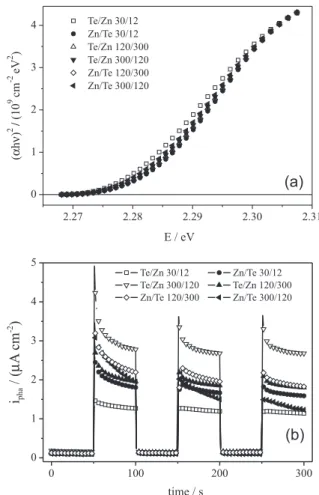
Figure 3 presents the plots of (αhν)2vs. hν obtained
from the diffuse diffraction spectrum (Figure 3a) and the chronoamperometric response to light on and off during polarisation at 0.2 V vs. open circuit potential for the different films (Figure 3b). The values of the photocurrent and the band gap determined from Figure 3 are shown in Table 2.
From Figure 3a, it is clear that the band gap values are practically the same for the different films. The average value is 2.28 eV, which is similar to that found in the literature for films produced by physical and electrodeposition techniques.9,28,29 This result indicates that
the films obtained are of type ZnTe, which absorb light next to orange.
The photocurrents vary for the different films but not significantly, except for the samples Te/Zn 30-12 and Te/Zn 120-300, which exhibit lower and higher photocurrent values, respectively. It can be said that the higher photocurrent values are observed for films where the percentage of Zn is increased. This occurs probably because the deposited Zn reacts with the excess of Te, forming a ZnTe phase and increasing the presence of the semiconductor in the deposits. It is worth noting that the photocurrent values obtained in this study are very significant, whereas the values of the order of nanoamperes are related to those in the literature for CdSe films.30
From SEM micrographs and by varying the intensity of the peaks in the Pt EDS measurements, it can be concluded that the films thickness of the various samples are different. Because the films are very thin, the photocurrent can vary over the sample volume. This work was not measured the thickness of the films, therefore was calculated relative thickness in order to make a comparison between different samples. To calculate comparative values of the thicknesses between the samples, a direct proportionality was assumed between the Pt peaks intensity in EDS spectra, considering that the maximum value for the depth is 1 µm. So, it was possible to obtain a comparative value of the films thicknesses and these values were used to calculate the
relative photocurrent per sample volume (r iphv). The values
of thickness and r iphv are shown in Table 2. It is emphasized
that the method used does not allow it to make absolute values of current per unit volume, but allows a comparison between different samples of ZnTe obtained in this work.
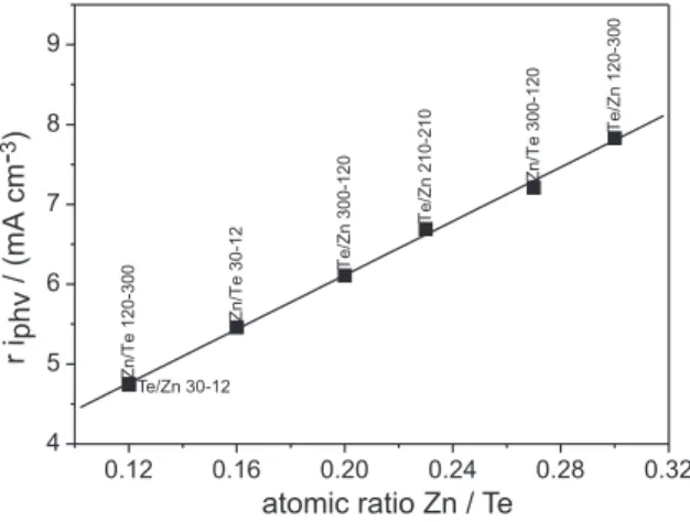
In Figure 4 are represented the variation of relative photocurrent per volume unit as function of film composition. The results are similar to those discussed earlier, where the photocurrent increases with the content of Zn in the film. It is noted that despite having obtained a straight this case, the relationship between photocurrent and composition need not necessarily to be linear, since the values used are relative thickness between the different samples.
Conclusions
ZnTe thin films were obtained by potentiostatic steps and aqueous solution. The morphology and film composition depend of deposition conditions, however the band gap value is not varied in the different experimental
Figure 3. (a) hν vs. (αhν)² for a spectral response obtained in the samples of ZnTe by UV-Vis that was describe on Table 1. (b) Chronoamperometry in light and dark applying a E = +0.20 V for 300 s in 0.1 mol L–1 ferrocene
+ 0.5 mol L–1 NaClO
4 in the middle of acetonitrile. Equilibrium time
conditions used in this work. Eg was of 2.28 eV, which is a value close to that of ZnTe bulk and ZnTe films produced by other techniques. SEM analyses showed a dendritic morphology with thick branches for samples with higher amounts of Zn in coating. Using an approximate method for calculating the relative thickness of the different samples was possible to observe that the photocurrent increases with the content of Zn in the film and the values obtained for all samples were the order of mA cm–3. This value indicating
that ZnTe obtained in this work is a promising material for use in pn-junctions.
Acknowledgments
The authors wish to thank the Brazilian funding institutions: CNPq (Process No. 2010/18134-5), CNPq and FAPESP (Processes No. 2009/00788-1; 2010/18134-5; and 2012/10947-2).
References
1. Colletti, L. P.; Thomas, S.; Wilmer, E. M.; Stickney, J. L.; Electrochem. Synth. Modifications Mater. 1997, 451, 253. 2. Wang, L.; Cao, L. X.; Su, G.; Liu, W.; Xia, C. H.; Zhou, H. J.;
Appl. Surf. Sci. 2013, 280, 673.
3. Fang, X. S.; Zhai, T. Y.; Gautam, U. K.; Li, L.; Wu, L. M.; Yoshio, B.; Golberg, D.; Prog. Mater. Sci. 2011, 56, 175. 4. Loh, L.; Dunn, S.; J. Nanosci. Nanotechnol. 2012, 12, 8215. 5. Janotti, A.; Van de Walle, C. G.; Rep. Prog. Phys. 2009, 72,
126501.
6. Fauzi, F.; Diso, D. G.; Echendu, O. K.; Patel, V.; Purandare, Y.; Burton, R.; Dharmadasa, I. M.; Semicond. Sci. Technol. 2013, 28, 045005.
7. Tanaka, T.; Nishio, M.; Ogawa, H.; Recent Progress in ZnTe-based green LED; Chen, N.P., eds Handbook of Light Emitting and Schottky Diode: New York, USA, 2009, ch. 15.
Figure 4. Relative photocurrent per volume unit values vs. atomic ratio Zn/Te in ZnTe thin films.
8. Mondal, A.; McCandless, B. E.; Birkmire, R. W.; Sol. Energy Mater. Sol. Cells 1992, 26, 181.
9. Mahalingam, T.; John, V. S.; Rajendran, S.; Sebastian, P. J.; Semicond. Sci. Technol. 2002, 17, 465.
10. Neumann-Spallart, M.; Koenigstein, C.; Thin Solid Films 1995, 265, 33.
11. Soundararajan, D.; Lim, Y.; Chun, M. P.; Kim, K. H.; Electron. Mater. Lett. 2013, 9, 177.
12. Spath, B.; Fritsche, J.; Sauberlich, F.; Klein, A.; Jaegermann, W.; Thin Solid Films 2005, 480, 204.
13. Rao, G. K.; Bangera, K.V.; Shivakumar, G. K.; Mater. Res. Bull. 2010, 45, 1357.
14. Chaure, N. B.; Nair, J. P.; Jayakrishnan, R.; Ganesan, V.; Pandey, R. K.; Thin Solid Films 1998, 324, 78.
15. Konigstein, C.; Neumann-Spallart, M.; J. Electroc. Soc. 1998, 145, 337.
16. Ishizaki, T.; Ohtomo, T.; Fuwa, A.; J. Phys. D: Appl. Phys. 2004, 37, 255.
17. Mahalingam, T.; Dhanasekaran, V.; Sundaram, K.; Kathalingam, A.; Rhee, J. K.; Ionics 2012, 18, 299.
18. Diso, D. G.; Fauzi, F.; Echendu, O. K.; Weerasinghe, A. R.; Dharmadasa, I. M.; J. Phys.: Conference Ser. 2011, 286, 012040. 19. Yutang, L.; Xilin, Z.; Ronghua, L.; Renbin, Y. C. L.;
Qingyun, C.; J. Solid State Chem. 2011, 184, 684.
20. Ishizaki, T.; Ohtomo, T.; Fuwa, A.; J. Phys. D: Appl. Phys. 2004, 37, 255.
21. Yang, Y. A.; Taggart, D. K.; Brown, M. A.; Xiang, C. X.; Kung, S. C.; Yang, F.; Hemminger, J. C.; Penner, R. M.; ACS NANO 2009, 3, 4144.
22. Patel, K. J.; Panchal, C. J.; Kheraj, V. A.; Desai, M. S.; Mater. Chem. Phys. 2009, 114, 475.
23. Ambily, S.; Menos, C. S.; Mater. Let. 1998, 34, 124. 24. Flowers, B. H.; Wade, T. L.; Garvey, J. W.; Lay, M.; Happek, U.;
Stickney, J. L.; J. Electroanalytical Chem. 2002, 525, 273. 25. Marczona, R.; Varga, K.; J. Radioanlytical Nucl. Chem. 2006,
269, 29.
26. Petrauskas, A.; Grinceviciene, L.; Cesuniene, A.; Matulionis, E.; Surf. Coat. Technol. 2005, 192, 229.
27. Jiang, Y.; Kou, H.; Li, J.; Yu, S.; Du, Y.; Ye, W.; Wang, C.; J. Solid State Chem. 2012, 194, 336.
28. Nishio, M.; Hayashida, K.; Guo, Q.; Ogawa, H.; Appl. Surf. Sci. 2001, 169, 223.
29. Lin, M. C.; Chen, P.Y.; Sun, I. W.; J. Electrochem. Soc. 2001, 148, C653.
30. Hus, S. M.; Parlak, M.; J. Phys. D: Appl. Phys. 2008, 41, 035405.
Submitted on: October 14, 2013
Published online: January 24, 2014