DIMENSIONAL EFFECT ON OPTICAL
PROPERTIES OF CADMIUM ZINC
TELLURIDE THIN FILMS
Dr. MONISHA CHAKRABORTY
Assistant Professor, School of Bio-Science & Engineering, Jadavpur University, 188, Raja S. C. Mallik Road, Kolkata-700032, India.
Abstract :
In this work, thin films of Cd1-xZnxTe of 1µm and 100nm thickness are fabricated on plain glass
substrates with ‘x’ varying from 0.0567 to 0.2210. Optical properties of these fabricated films are studied. The optical properties of these films vary with thickness and ‘x’. The present paper has dealt with the estimation of dimensional effect on Cd1-xZnxTe thin films in the light of optical characterization studies.
Keywords: Dimensional effect; Optical properties; Thin films; Cd1-xZnxTe
1. Introduction
High resistivity II-VI compound semiconductor e.g. ZnTe, CdTe and their alloys Cd1-xZnxTe with
stoichiometric value ‘x’ are the potential materials used for room temperature X-ray and Gamma ray detectors, infrared detectors, solar cells and other optoelectronic devices [1-5]. Introduction of Zn into CdTe makes the lattice of Cd1-xZnxTe tunable and by adjusting the Cd/Zn ratio, a lattice-matched substrate for the growth of the
HgCdTe epitaxial layer has been reported in [6]. In the recent years, major attention has been given to the investigation of optical, structural and electrical properties of Cd1-xZnxTe thin films in order to improve the
performance of the device and also for finding new applications. Designable semiconductor band gap is helpful for controlling the resistivity as well as the valence and conduction band alignment at the semiconductor interface. CdTe/CZT-based surgery probes have large impact on patient management in surgical oncology. Excellent large-field of view modules have already been realized as reported in [7]. The performance of a CZT dual Positron Emission Tomography (PET), dedicated for breast cancer, is studied by a group of researchers and these are reported in [8]. Studies in [9] report on dedicated emission mammotomography with CZT imaging detector. A comprehensive review of the material properties of Cd1-xZnxTe with varying zinc content is reported
in [10]. Some studies on the structural and optical properties of II-VI compound semiconductors are proposed previously and these are reported in [11-19]. The range of ‘x’ in Cd1-xZnxTe lies preferably within 0.05≤ ‘x’ ≤0.95 [19, 20]
.
In the present work, Cd1-xZnxTe thin films of 1µm and 100nm thickness for ‘x’ varying from 0.0567 to
0.2210 are fabricated on plain glass substrates. These films are subjected to optical characterization studies. The method to determine the variation of band gap energy with concentrations of zinc has been repoted in [21]. In the present paper, the variation of band gap of Cd1-xZnxTe 1µm and 100nm thin films with the experimentally
designed values of ‘x’ are obtained. Photoluminescence (PL) is a suitable technique to determine the crystalline quality and the presence of impurities in the material. In the present work, the PL spectra of the Cd1-xZnxTe 1µm
and 100nm thin films are obtained. Film properties change with ‘x’ and these also change with the change in the thickness of the film.
In this work, proper methods are adopted to fabricate Cd1-xZnxTe thin films of 1µm and 100nm
thickness and these are discussed in section 2 of this paper. The mathematical calculation for obtaining experimentally designed value of ‘x’ is discussed in section 2.1 of this paper. The optical characterization results of Cd1-xZnxTe thin films of 1µm and 100nm thickness are discussed in section 3 of this paper. PL spectra of the
Cd1-xZnxTe 1µm and 100nm thin films are studied and these results are discussed in section 3.1 of this paper
The significance of the results of this work is discussed with respect to dimensional effect in section 4 of this paper. The work is concluded in section 5 of this paper.
2. Materials and Methods
In this work, physical deposition method is adopted to fabricate large area Cd1-xZnxTe thin films of
dimensions 23 mm x 37 mm x 1 mm are dipped in chromic acid for two hours. These are washed with detergent and finally ultrasonically cleaned with acetone before use.
In order to design the six different compositions of Cd1-xZnxTe thin films of 1µm and 100nm thickness, six different % ratio of the stack layer of ZnTe/CdTe is chosen and these are 20:80, 30:70, 40:60, 50:50, 60:40 and 70:30. For these six ratios of the stack layer of ZnTe/CdTe, six different values of ‘x’ are obtained. The mathematical detail is discussed with a sample calculation in section 2.1 of this paper.
For the film fabrication, 500W RF Sputtering unit has been used. ZnTe and CdTe targets are placed in the target holders of the RF sputtering unit. Plain glass substrates are kept at the bottom of the target holder and temperature to the order of 100°C is maintained on the substrates. Argon gas is injected from outside and pressure of the order of 10-2 Torr has been maintained. At this pressure, the RF unit is energized and a power of 500W with a frequency of 13.56 MHz is applied between the target and the substrate. On application of this RF power the target gets energized and vapour of the target material produced deposits on the substrate. At the substrate temperature the film gets crystallized and the thickness is dependent on the sputtering time. Both CdTe and ZnTe targets are sputtered sequentially and a stack layer of ZnTe/CdTe is thus obtained. The stack layer is then annealed in vacuum (10-5 Torr) for an hour at 300°C. Both Cadmium and Zinc tried to inter-diffuse among each other to get into a stabilized state. Applications of thermal energy initiate both cadmium and zinc inter-diffusion. However, the stoichiometric ratio of cadmium and zinc is not equal and as a result the film is formed in the form of Cd1-xZnxTe. The value of ‘x’ decides whether the film is CdTe or ZnTe. Thickness and deposition time for CdTe and ZnTe layers for each composition of Cd1-xZnxTe films of 1µm thickness are tabulated in Table 1(a). Similarly, thickness and deposition time for CdTe and ZnTe layers for each composition of Cd 1-xZnxTe 100nm thin films are tabulated in Table 1(b).
Table 1(a) Thickness and Deposition Times of ZnTe and CdTe layers in 1µm CZT Films
Table 1(b) Thickness and Deposition Times of ZnTe and CdTe layers in 100 nm CZT Films
2.1. Sample Calculation of ‘x’
In this section, the mathematics to determine ‘x’ in Cd1-xZnxTe thin film is discussed with a sample calculation. For this purpose, one out of the six samples is considered and this is a 1µm stack of CZT comprised of ZnTe film deposited on CdTe film. Percentage thickness ratio of ZnTe : CdTe layer is 60:40 and this can be expressed as given in Eq. (1.1).
S..No. (%ZnTe):(%CdTe) Thickness of ZnTe layer TZnTe (nm) Thickness of CdTe layer TCdTe (nm) Deposition time of CdTe layer
tCdTe
Deposition time of ZnTe layer
tZnTe Fraction of Zinc in CZT matrix, ‘x’ 1 20:80 156.48 843.52 10 mins 49 sec 3 mins 29 sec 0.0567 2 30:70 241.29 758.71 9 mins 44 sec 5 mins 22 sec 0.0870 3 40:60 330.97 669.03 8 mins 35 sec 7 mins 21 sec 0.1182 4 50:50 425.95 574.05 7 mins 22 sec 9 mins 28 sec 0.1510 5 60:40 526.74 473.26 6 mins 4 sec 11 mins 42 sec 0.1865 6 70:30 633.88 366.12 4 mins 42 sec 14 mins 5 sec 0.2210
S.No. (%ZnTe):(%CdTe) Thickness of ZnTe layer TZnTe (nm) Thickness of CdTe layer TCdTe (nm) Deposition time for CdTe layer
tCdTe
Deposition time for ZnTe layer
tZnTe Fraction of Zinc in CZT matrix, ‘x’
1 20:80 15.65 84.35 1 min 5 sec 21 sec 0.0567
2 30:70 24.13 75.87 58 sec 32 sec 0.0870
3 40:60 33.10 66.90 51 sec 44 sec 0.1182
4 50:50 42.60 57.40 44 sec 57 sec 0.1510
%
60
%
40
ZnTe ZnTe ZnTe CdTe CdTe CdTem
n
M
ZnTe
m
CdTe
n
M
(1.1)where,
mZnTe and mCdTe are the masses of ZnTe and CdTe layers respectively to attain the % ratio ZnTe : CdTe as 60:40. MZnTe and MCdTe are the molar masses of ZnTe and CdTe respectively and these values are MZnTe =193 gms/mol and MCdTe=240 gms/mol. On putting these values, Eq. (1.1) becomes,
.
. .240
1.5
.
. .193
ZnTe ZnTe CdTe CdTe
T
A
T
A
(1.2)where,
‘A’ is the cross-sectional area of the substrate. ρZnTe and ρCdTe are the density of ZnTe and CdTe layers respectively and these values are ρZnTe = 6.34 gms/cc and ρCdTe=5.85 gms/cc. TZnTe and TCdTe are the values of thickness of ZnTe and CdTe layers respectively. On putting these values, Eq. (1.2) becomes,
1.113022477
ZnTe
CdTe
T
T
(1.3)1
ZnTe CdTe
T
T
m
(1.4)Solution of Eq. (1.3) and Eq. (1.4) gives the values of the thickness of CdTe and ZnTe layers and these are, TCdTe = 473.26 nm and TZnTe = 526.74 nm. (1.5 a) Deposition rates for CdTe and ZnTe targets are 78 nm/min and 45 nm/min respectively. (1.5 b) From Eq. (1.5 a) and Eq. (1.5 b) the deposition times for CdTe and ZnTe layers for this sample are obtained and these values are tCdTe = 6 mins 4 sec and tZnTe = 11 mins 42 sec respectively. (1.5 c) So, mass of ZnTe layer, mZnTe = 3339.53.A.10-7 gms
and mass of CdTe layer, mCdTe = 2768.57.A.10-7 gms. Molar mass of Zinc, MZn = 65.38 gms/mol.
So, 1139.29.A.10-7 gms of zinc is present in 3339.53.A.10-7 gms of ZnTe.
Fraction of zinc in this CZT matrix =7
7
1139.29. .10
0.1865
(2768.57 3339.53). .10
A
A
(1.6)Similarly, for other % ratios of ZnTe : CdTe layers for both the thickness domains considered in this study, the values of ‘x’ are calculated and these results are tabulated in Table 1(a) and Table 1(b).
3. Optical Characterization and Results
The samples of Cd1-xZnxTe 1 m and 100nm thin films are subjected to optical characterization studies. Transmission and reflection spectra of these samples have been recorded using PerkinElmer Lambda 35 spectrophotometer and the plots of normalized values of (αh )2 vs. h are obtained. Sample plots showing the variation of (αh )2 vs. h obtained from 1 m and 100nm Cd1-xZnxTe thin films for ‘x’ = 0.1865 are shown in Fig. 1(a) and Fig 1(b) respectively as sample results. From such curves, energy band gap of the fabricated films can be evaluated [10, 19, 21]. The relation between the absorption coefficient (α) and the incident photon energy hυ is given by,
(αh )2 = A(h -Eg) (1.7) where, A is a constant and Eg is the band gap energy.
Fig. 1(a) Variation of (αh )2 vs. h of Cd
1-xZnxTe 1 m thin film at ‘x’ = 0.1865
Fig. 1(b) Variation of (αh )2 vs. h of Cd
1-xZnxTe 100nm thin film at ‘x’ = 0.1865
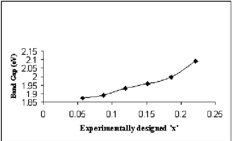
Fig. 2(b) Variation of band gap energy with ‘x’ for Cd1-xZnxTe 100 nm thin films
3.1.Photoluminescence Results
Photoluminescence (PL) spectra for Cd1-xZnxTe 1 m and 100 nm thin films, deposited on glass substrate, are obtained for different ‘x’, with photo-excitations at 500 nm for 1 m thin films and 450nm for 100nm thin films. PL studies are done using PerkinElmer LS 55 luminescence spectrometer. The typical comparative plots of room temperature PL spectra of Cd1-xZnxTe 1 m and 100nm thin films for ‘x’ = 0.1865 are shown in Fig. 3 as sample results.
Fig. 3 Room Temperature PL spectra of Cd1-xZnxTe (1) 1 m and (2) 100 nm thin films at ‘x’ = 0.1865
Similarly, for other values of ‘x’, such comparative plots of room temperature PL spectra of Cd
1-xZnxTe 1 m and 100nm thin films are obtained.
4. Discussion
property of Cd1-xZnxTe 100 nm thin films must have decreased due to nano-structured dimensional effect. These PL results indicate that thickness has a good correlation to the reflection property of the fabricated films.
5. Conclusion
This study infers that dimensional effect has impact on optical properties of Cd1-xZnxTe thin films.
Acknowledgments
Author is thankful to all the members of Advanced Materials and Solar Photovoltaic Division, School of Energy Studies, Jadavpur University, Kolkata, India for their help and cooperation.
References
[1] Dornhaus, R.; Nimitz, G.; Höhler , G. and Nickisch, E. A. (1983). Springer, p-119. [2] Faurie, J. P.; Reno, J. and Boukerche, M. (1985). J. Crystal Growth, 72, p-111.
[3] Willardson, R. K. and Beer, A. C. (1978). Semiconductors and Semimetals, 13, Academic, New York. [4] Schlesinger, T. E. and James, R. B. (1995). Semiconductors and Semimetals edited 43, Academic, San Diego. [5] Shi, Z. Q.; Stahle, C. M. and Shu, P. (1998). Proc.SPIE, 90,p- 3553.
[6] Guergouri, K.; Ferah, M. S.; Triboulet, R. and Marfaing, Y. (1994). J. Cryst.Growth, 6, p-139. [7] Eisen, Y.; Mardor, I.; Shor, A. et al. (2002): IEEE Trans. Nucl. Sci., 49, p-172.
[8] Peng, H.; Olcott, P. D.; Pratx, G.; Foudray, A. M. K.; Chinn, G.; Levin, C. S. (2007): IEEE Nuclear Science Symposium Conference Record.
[9] Brzymialkiewicz, C. N.; Tornai, M. P.; McKinley, R. L. and Bowsher, J. E. (2005):IEEE Transactions on Medical Imaging, 24, p-7. [10] Schlesinger, T. E.; Toney, J. E.; Yoon, H.; Lee, E. Y.; Brunett, B. A. ; Franks, L. and James, R. B. (2001). Material Science and
Engineering 32, p-103.
[11] Patidar, D.; Rathore, K. S.; Saxena, N. S.; Sharma, K. and Sharma, T. P. (2008). Chalcogenide Letters 5, p-21.
[12] Rao, K. P.; Md. Hussain, O.; Reddy, K. T. R. ; Reddy, P. S.; Uthanna, S. ; Naidu, B. S. and Reddy, P. J. (1995). Journal of Alloys and Compounds, 218, p-86.
[13] Samanta, B.; Sharma, S. L. and Chaudhuri, A. K. (1995). Vacuum, 46, p-739. [14] Li, M. and Li, J.C. (2006). Materials Letters 60, p-2526.
[15] Herrera, S.; Ramos, C. M.; Patino, R..; Pena, J. L.; Cauich, W.; Oliva, A. I. (2006). Brazilian Journal of Physics, 36.
[16] Nag A.; Sapra, S.; Sen Gupta, S.; Prakash, A.; Ghangrekar, A.; Periasamy, N.; Sarma, D. D. (2008). Bull. Mater. Sci., 31, p-561. [17] Rao, C. N. R. ; Kulkarni, G. U. ; Thomas, P. J. ; Edwards, P. P. (2002). Chem. Eur. J 8, p-29.
[18] Reno, J. L. and Jones, E. D. (1992). Phys. Rev. 45, p-1440.
[19] Chakraborty, M. (2011). International Journal of Engineering Science and Technology, 3, 5, pp- 3798-3806. [20] Weblink: http://www.freepatentsonline.com/5528495.