Abstract—This paper shows the design and post-layout simulation of an integrated analog-to-digital interface for energy quality meter systems, in which voltages and currents are sampled and converted to digital values for later digital processing by a fully integrated system or discrete DSP. It has been used the switched capacitor technique on the sampling and conversion circuits, instead of the analog conventional techniques, thus reducing the circuit size and achieving a higher precision. The proposed analog front-end was successfully simulated in a 0.35-um AMS CMOS process. The system has six input channels and can reach 10 bits of resolution at a sampling rate of 369,000 words per second. The circuit takes an area of 5.2 mm2, including pads
Index Terms— analog-to-digital conversion, current sampling, digital signal processing, energy quality metering, voltage sampling
I. INTRODUCTION
HEN nonlinear load in the power system is rapidly increased, especially after the extensive use of power electronic devices, ultra-harmonics are greatly produced in the power grid, which cause the serious power quality deterioration and threaten the power system security and economic operation. When using currently existing induction and electronic meters, non-harmonic source users absorb the unnecessary and even harmful harmonic electric energy; moreover, they have to pay for it. On the contrast, harmonic source users transform part of fundamental waves into harmonic energy, which pollutes power grid, and avoids the corresponding electric bills. So it is obvious that electric energy measurement data is the settlement basis between power generation, power transmission and distribution, and power consumer [1]. However, power harmonic leads to inaccurate measurement and unfair charges, which seriously harm the power supply system and the nonharmonic source users' interests, and directly influence the accuracy and fairness of electric energy measurement. Therefore, it is necessary for power industry to measure and analyze harmonic energy accurately in order to provide harmonic
Manuscript received March 28, 2014; revised July 15, 2014. This work was supported in part by CNPq/Brazil.
E. D. C. Cotrim is with the Federal University of Itajuba – Itabira Campus, Itabira, MG 35903-087 Brazil. (phone: (+55) 31-3839-0875; e-mail: evandro.cotrim@ unifei.edu.br).
L. H. C. Ferreira is with the Systems Engineering & Information Technology Institute, Federal University of Itajuba, Itajuba, MG 37500-903 Brazil. (e-mail: [email protected]).
T. C. Pimenta is with the Systems Engineering & Information Technology Institute, Federal University of Itajuba, Itajuba, MG 37500-903 Brazil. (e-mail: [email protected]).
energy measurement products with high accuracy, multi-rate and multi-function for the current power grid.
This work presents the design and post-layout simulation of an integrated analog to digital system that samples voltage and current from the grid and converts this measurements to digital for further digital processing, where calculations such harmonic distortion and power consumption can be performed using Fast Fourier Transform.
The paper is organized as follows. Section II describes the concepts and architecture of the system. Section III presents the results and the prototype layout. Conclusions are drawn in section IV.
II. SYSTEM ARCHITECTURE
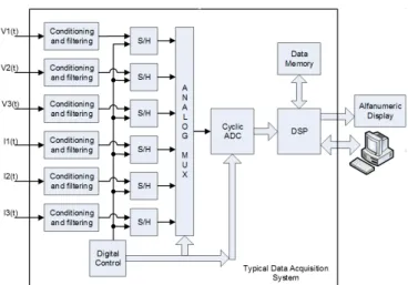
Advanced power-grid monitoring systems combine many functions in order to enable safe and efficient power delivery. These systems track the voltage and current on multiple phases, where the acquisition must be synchronized in order to meet stringent standards requirements and to accurately measure power factor and other energy-related values [2]. In a typical scheme, each phase’s instant current and voltage are acquired by current transformers (CT) and voltage transformers (VT), respectively. They provide high-voltage insulation and reduce both high-voltage and current to compatible levels that can be handled by the internal circuits. The signal conditioning circuit makes the sampled signal voltages compatible to in-chip voltages. Additionally, a second-degree Sallen-Key low-pass filter, the higher sampled harmonics are attenuated thus the aliasing distortion during discretization is minimized. The sample-and-hold circuit acquires each phase’s data simultaneously and keeps it stable in order to have it data applied to the analog-to-digital converter. The analog-to-digital converted data is then stored in a memory stack, in order to allow later calculations of the active, reactive and apparent-power, power-factor and harmonic distortion by a DSP system [2]. Additionally, the stored instant voltage and instant current values can be later recovered in order to determine overcurrent or overvoltage occurrences in the power system. As shown in Fig. 1, V1(t) to V3(t) inputs are the phase voltages present at the grid, while I1(t) to I3(t) are related to the current values flowing through the system. As the converter’s speed is very faster than the sampled signal’s frequency, the signals are applied to the same analog-to-digital converter through an analog multiplexer, saving chip area. In this architecture, the analog multiplexer is embedded into the ADC converter.
An Integrated Analog Front-end for Energy
Quality Meter Systems
Evandro D. C. Cotrim, Luis H. C. Ferreira, and Tales C. Pimenta
W
Proceedings of the World Congress on Engineering and Computer Science 2014 Vol I WCECS 2014, 22-24 October, 2014, San Francisco, USA
ISBN: 978-988-19252-0-6
ISSN: 2078-0958 (Print); ISSN: 2078-0966 (Online)
The analog values converted to digital format are made available either to a DSP system or a memory stack through direct-memory access system (DMA), for later processing. Additionally, the sampled data can be transmitted to a personal computer or PDA, by a communication port.
A. Signal conditioning and filtering circuit
The input signals sampled by the VT end CT must be applied to a conditioning and filtering circuit so the voltage and current values are reduced and made compatible to the in-chip supported values. The current signal sampled through the CTs is converted to voltage by means of a hall sensor, but if desired a current-to voltage circuit can be implemented on-chip as well. The filter is responsible for superior harmonics attenuation and for avoiding the aliasing distortion on the sampled signal. The Sallen-Key filter has been used in this application, once it has a constant quality factor Q and is independent of R and C variations, not affecting the flatness of the passband, nor permit aliasing [3]. As it is desired a decrease of – 40-dB per decade on the passband attenuation, a second-degree Sallen-Key filter [3] has been implemented. Since the passband and stopband specifications must be met even under worst-case tolerance conditions, the antialiasing filter is usually overdesigned [3]. R and C values may vary up to 50% thus a typical 1500-Hz passband may vary from 750-Hz up to 2.25-kHz. Taking these variations in account, R and C are calculated in a way that a passband of 1500 Hz is allowed even when they present their minimum value, once it is desired to sample up to the 25th harmonic component of the input signal. Under these conditions, for the typical case, the passband becomes equal to 2.25-kHz, even lower than the 1.5-MHz sampling frequency, avoiding aliasing distortion.
B. Sample-and-Hold Circuit
Sample-and-hold circuit is responsible for sampling the input signals and keeping they stable while acquired by the analog-to-digital converter during the beginning of the conversion. In power-factor calculations, where the misalignment between instantaneous voltage and current is determined, it is also important to guarantee that the phase current and voltage are sampled synchronously, so calculations errors are avoided. Thus the sample-and-hold circuits must sample the input signals synchronously. If they are sampled in different time, calculations must be
performed in order to compensate the time between each channel’s input sampling.
The system precision depends directly of the sampled signal correctness when the sample-and-hold receives the hold control signal, where the exact voltage value of the signal present at its input must be presented at its output. When the circuit receives the hold command, MOS switches are closed and open, so undesired charges are injected in the circuit resulting in voltage errors.
Using switched-capacitor techniques and appropriate techniques allow error-cancelling due to charge-injection effect and offset-error cancellation [4], [5]. We have implemented the sample and hold circuit and the switching sequence described in [4]. Fig. 3 depicts the simulated sample-and-hold output waveform.
C. Analog-to-Digital Converter
This circuit is responsible for converting the sampled analog data to the digital format. Due to the relatively lower sampled frequency, a compact and slower analog-to-digital converter is used. Cyclic analog-to-digital converters (ADCs) are used in moderate-to-high-accuracy and low-to-moderate-frequency applications, especially where low power consumption and low area occupation is required [6], [7]. In a cyclic ADC, the residue signal is cyclic, thus only one stage is needed, and N periods are required to convert an N-bit digital code. In these ADCs, noise and accuracy requirements decrease from the most-significant bit (MSB) to the least-significant bit (LSB) cycle, but the invested
Fig. 1. Example of a fully data acquisition system architecture.
Fig. 2. Implemented system.
Fig. 3. Input, hold and output voltages – Sample-and-hold circuit.
Proceedings of the World Congress on Engineering and Computer Science 2014 Vol I WCECS 2014, 22-24 October, 2014, San Francisco, USA
ISBN: 978-988-19252-0-6
ISSN: 2078-0958 (Print); ISSN: 2078-0966 (Online)
energy per cycle is “conventionally” constant [8]. The main disadvantage of this mode of operation is the long conversion cycles, which is exacerbated by the need to use closed-loop amplifiers instead of comparators [9].
After filtering and sampling operations, the sampled signals from the six input channels are converted to the differential form [9] and applied to a 12-to-2 multiplexer, where its differential outputs are applied to the ADC for converter. The ADC topology is also based in switched-capacitor techniques, allowing the charge-injection effect during switching and offset independent [8].
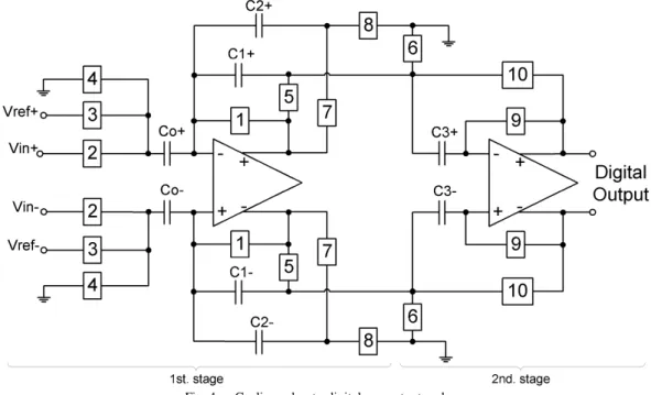
The cyclic ADC circuit is implemented by the two-stage differential circuit depicted in Fig. 4. The switches numbered from 1 to 10 are implemented by MOS transistors with dummy elements in order to prevent charge injection. During cyclic conversion, each output bit is available after three cycles of clock and the switching sequence that performs the analog-to-digital conversion is depicted in Table I. The next switching sequence depends on the value of the previously converted bit B(i). At the beginning of the conversion cycle, operation (I) is performed and the MSB is derived [8].
Fully-Differential Folded Cascode OTA
A fully-differential folded cascode OTA with capacitive common-mode feedback circuit (CMFB) has been implemented in this converter [10]. This topology is largely used due to its simplicity, symmetry, speed, lower power consumption and improved PSRR in spite its limited output voltage range, when compared to a two-stage amplifier [11]. The implemented amplifier presented an open-loop gain of 85.4-dB, a phase margin of 82.2 degrees and a 0-dB frequency of 52.3-MHz.
III. SYSTEM SIMULATION
The proposed system has been simulated using Accusim© Mentor Graphics tool after parasitic layout extraction and the circuit layout was built in AMS 0.35-µm CMOS technology implemented using Mentor ICStation©. The implemented circuit was simulated using a 60-Hz/3.5-Vpp sinusoidal signal as input voltage with offset equal to 1.75-Vdc. The circuit was designed to work with a 5-Vdc supply voltage and VREF set to half scale of the maximum input signal voltage (3.5-Vdc). By measuring the voltages at the sample-and-hold output, a mean error of only 0.05% was obtained. At the ADC output, in a range of 1024 possible digital words for each channel, only 10 results presented a deviation of ± 1 LSB from the correct value.
Due to the mixed analog and digital nature of the circuit, some precautions must be taken in order to avoid that switching noise generated by digital circuitry reaches analog portion of the system. To do so, the analog section has been built inside an N-well guard-ring and the power supply rails were connected to distinct pads
The same measures have been taken regarding the digital circuitry. These measures decrease the coupling of the switching noise through the substrate and by power supply rails, respectively.
The digital circuitry were implemented using minimal- dimension transistors and the analog section using larger gate length transistors in order to minimize DIBL (drain-induced barrier lowering) effect [12].
The operational amplifiers have been implemented using matched transistors in order to reduce the offset and current mismatching and implemented inside an N-diffusion guard rings in order to reduce noise coupling through the substrate. The matched capacitors were implemented using a double-poly structure with dummy elements in order to prevent capacitor mismatch. The capacitors matrix is built inside an N- diffusion guard ring, to avoid switching noise coupling to the amplifiers. In order to minimize control signal crosstalk, the analog sections have been implemented in a way to avoid analog and digital buses crossings or superposition.
These measures aimed to minimize cross coupled noise signals that could jeopardize circuit’s accuracy or even functionality. Fig. 5 depicts the circuit layout, where the digital portion is at the upper side of the figure. The circuit occupied an area of 5.2-mm2 including pads. The circuit area with no pads is 1.98-mm2.
IV. CONCLUSION
This paper presented the design and simulation of an analog to digital interface for energy quality meter systems, where the voltage and current of a three-phase system is sampled and converted to digital for further digital signal processing.
The converted data is used to assess power grid quality related measurements such as voltage and current surges, under voltage and over voltage occurrences, power consumption, power factor, harmonic distortion among surges and total harmonic distortion. The system is comprised by a signal-conditioning circuitry which reduces the sampled current and voltages to acceptable in-chip values and filters the input signals in order to avoid aliasing effect and superior harmonics blocking.
The system is comprised by a signal-conditioning circuitry which reduces the sampled current and voltages to acceptable in-chip values and filters the input signals in order to avoid aliasing effect and superior harmonics blocking. The sample-and-hold circuitry allows a
TABLEI
ADCSWITCHING SEQUENCE FOR EACH OUTPUT BIT
Proceedings of the World Congress on Engineering and Computer Science 2014 Vol I WCECS 2014, 22-24 October, 2014, San Francisco, USA
ISBN: 978-988-19252-0-6
ISSN: 2078-0958 (Print); ISSN: 2078-0966 (Online)
synchronized sampling of the six input channels and a cyclic analog-to-digital converter, suitable for low-frequency operation is implemented in the system. The use of the cyclic algorithm saves a significant amount of silicon area once the circuit size is independent of the number of converting bits and allows a more precise operation, once the results are independent of the capacitor-ratio and operational amplifiers’ offset. Differential topology of the ADC improved the circuit precision once the clock feedthrough and the charge injection effects on the MOS switches are common-mode occurrences and minimized by the cyclic topology and the deployment of MOS switches with dummy transistors. Simulation showed a maximum error of 0.05% after the sample-and-hold section and a deviation of ± 1-LSB in only 10 values, among the 1024 possible output values at the ADC output.
The circuit was implemented in a 0.35- m process and occupied a total area of 5.2-mm2 including pads. If used as a block in a fully-integrated DSP system, this circuit with no pads occupies an area of 1.98-mm2.
REFERENCES
[1] L. Zhi-kun, W. Quan, X. Xian-young and G. Yun-peng, "Design of harmonic energy meter based on TDK+DSP+MCU", 2012 International Conference on Measurement, Information and Control (MIC) , pp. 874 - 878, May, 2012.
[2] Maxim, "Power-grid monitoring" [Online] Available:
http://www.maximintegrated.com/solutions/guide/smart-grid/power-grid-monitoring.pdf.
[3] R. Gregorian, G. C. Temes, "Analog MOS Integrated Circuits for Signal Processing"; John Wiley & Sons, New York, 1986.
[4] K. Watanabe, K.; Ogawa, S.; "Clock-feedthrough Compensated Sample/Hold Circuits", Electronics Letters, 1988, Vol. 24, n. 19, pp. 1226-1228.
[5] R. C. Yen, and P. R. Gray, " A MOS Switched-capacitor Instrumentation Amplifier", IEEE J. Solid-State Circuits, 1982, SC-17, pp. 1008-1013.
[6] J-K. Woo et al, "A comparator-based cyclic analog-to-digital converter with boosted preset voltage", International Symposium on Low Power Electronics and Design (ISLPED), 2011, pp. 199-204. [7] M. Zaare', R. Lotfi, and M. Maymandi-nejad, "Capacitor scaling for
low-power design of cyclic analog-to-digital converters", Proceedings of IEEE International Symposium on Circuits and Systems (ISCAS), 2010, pp. 1456 - 1459.
[8] H. Onodera, T. Tateishi, K. Tamaru, "A cyclic A/D converter that does not require ratio-matched components", IEEE Journal of Solid-State Circuits, vol. 23, n. 1, pp. 152-158, February 1988.
[9] B. Carter, "A Differential Op-Amp Circuit Collection"; Application Report SLOA064; Texas Instruments, July 2001; pp. 10-13. [10] S. M. Mallya, J. H. Nevin, "Design Procedures for a Fully-differential
Folded Cascode CMOS Operational Amplifier", IEEE Journal of Solid-State Circuits, vol. 24, n. 6, pp. 1737-1740, December, 1989. [11] F. Dülguer, E. Sáchez-Sinencio, J. Silva-Martinez, "A 1.3-V 5mW
fully integrated tunable bandpass filter at 2.1GHz in 0.35-?m CMOS", IEEE Journal of Solid-State Circuits, 2003, Vol. 38, n. 6, pp. 918-928.
[12] L. H. de Carvalho Ferreira, T. C. Pimenta, "A CMOS reference voltage based on threshold voltage for ultra low-voltage and ultra low-power", The 17th International Conference on Microelectronics (ICM 2005), 2005, pp. 10-12.
Fig. 4. Cyclic analog-to-digital converter topology.
Fig. 5. Circuit implemented in AMS 0.35 m technology.
Proceedings of the World Congress on Engineering and Computer Science 2014 Vol I WCECS 2014, 22-24 October, 2014, San Francisco, USA
ISBN: 978-988-19252-0-6
ISSN: 2078-0958 (Print); ISSN: 2078-0966 (Online)