A BIST Scheme for RF Power Amplifiers
J. Machado da Silva, A. Gabriel Pinho, Pedro F. Mota
Universidade do Porto, FEUP / INESC Porto
Rua Dr. Roberto Frias, 4200-465 Porto, Portugal
jms@fe.up.pt
Abstract
One can find today system-on-chip devices comprising also radio-frequency blocks. These highly integrated cir-cuits raise extraordinary challenges for testing, jeopardiz-ing the low cost requirements associated often to these products. A built-in self test scheme for RF power ampli-fiers based on a polynomial fitting approach is proposed here, which takes advantage of the existing local oscillator, up-conversion mixer, and pre-driver, allowing for low area overhead and performance degradation. Simulation and experimental results for gain and linearity (1 dB compres-sion and third order interception points) obtained with a GaAs distributed amplifier are presented which confirm the validity of the method. The BIST scheme proposed for im-plementing this method on-chip is then described, together with preliminary simulation results.
1. Introduction
The progress attained with submicron CMOS technolo-gies allows today not only to fully integrate RF transceivers on a single silicon substrate, but also to integrate these with the baseband (BB) processing and user interface func-tions [10, 1]. With the capability and benefits of monolithic integration being now extended to RF circuits, the acces-sibility to test nodes for control and observation is becom-ing more and more difficult as generatbecom-ing, propagatbecom-ing, and measuring high frequency signals is more acute [2].
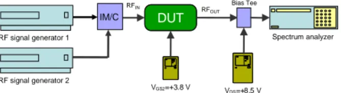
Figure 1 shows a typical set-up to perform single tone or two tone measurements. Besides the RF signal gen-erators, bias sources, and measurement instruments, im-pedance matching couplers and attenuators are required to interface the different devices. In the two tone case an im-pedance matching and combiner (IM/C) coupler is required to add the two signals and avoid interaction between the two RF generators. New test procedures are then required to avoid the necessity for complex and delicate set-ups and which allow testing embedded RF circuits.
This issue has deserved the attention from the research community and different solutions have already been pub-lished [9, 5, 11, 8, 3]. These works have addressed mainly Low Noise Amplifiers, or the transmitter and receiver sub-systems as a whole making it difficult to diagnose defective RF macros. In particular, the test of power amplifiers (PAs) has not been addressed with the same effort.
Spectrum analyzer RF signal generator 1 VDS=+8.5 V DUT RFIN RF OUT Bias Tee VGS2=+3.8 V IM/C RF signal generator 2
Figure 1.Typical RF power amplifier test set-up.
PAs are usually tested for linearity, output power, gain, and power added efficiency (PAE) using a single tone stim-ulus. Two-tone or more complex digital modulated signals are used to measure parameters such as intermodulation distortion (IMD) and adjacent channel leakage power ra-tio (ACPR). However, at the producra-tion stage typical tests include gain, output power, P1dB, and input return loss.
In [12] a PA test methodology based in the analysis of the transient response of the PA’s dynamic power supply cur-rent (iDD) is proposed for faster production test. Parameters
such as gain and PAE are estimated after the iDD
signa-ture using non-linear regression functions computed using multivariate adaptive regression splines. The amplifier un-der test parameters are estimated by using these regression function to map the observed transient current to the corre-sponding specifications. The method requires then testing a number of known good devices to provide the mapping regression functions.
In this paper a method to test for power and linearity, after the estimation of 1 dB compression (P1dB) and 3rd
order input interception (IIP3) points is presented, which is suitable to be built on-chip. The performed measure-ments provide directly an estimation of these parameters. Simulation and experimental results obtained with a GaAs distributed amplifier are shown which confirm the valid-ity of the method. Concerning on chip implementation, as a single tone stimulus is employed, the existing local os-cillator can be used as stimulus generator. To propagate this stimulus into the PA, instead of creating an alternative path using additional switches (which could degrade per-formance), a reconfigurable up-conversion mixer is used to route the stimulus to the PA input. Advantage is also taken of the existing variable gain PA driver to control the ampli-tude of the stimulus at the PA’s input. Simple diode based power detectors are used to obtain DC measures of the PA’s input and output powers. These measures are then used off-chip to compute the polynomial that best fits the PA’s
gain characteristic, whose coefficients allow us to obtain P1dB and IP3. As only DC and digital control signals are
needed to be interchanged with the tester, general purpose test infrastructures can be used for control and observation purposes.
Next section reviews the mathematics behind the com-putation of P1dBand IP3 values after the polynomial fitting
coefficients. Section 3 presents simulation and experimen-tal results obtained with a GaAs distributed amplifier. Sec-tion 4 describes the implementaSec-tion of the method on chip, and presents simulation results obtained with the IC proto-type being designed. Finally, section 5 highlight the main conclusions.
2. Polynomial-Fitting Testing Method
The output response of an amplifier with weak non-linear behaviour can be modelled as a Taylor series in terms of the input voltage:
vout= a0+ a1vin+ a2v2in+ a3v3in+ ... (1)
The Taylor series model is valid for memoryless non-linear functions, while Volterra series are required when memory effects have to be included. Nevertheless, the Taylor series model is applicable when the number of stages is small.
If a single frequency signal vin= Acos(ωt) is applied at
the input, the output voltage becomes
vout= a0+ a1Acos(ωt)+a2A2cos2(ωt)+
a3A3cos3(ωt) + ... = = (a0+ 1 2a2A 2) + (a 1A+ 3 4a3A 3)cos( ωt) +1 2a2A 2cos(2 ωt)+1 4a3A 3cos(3 ωt) + ... (2)
The voltage gain at frequencyω0, retaining only terms
up to the third order, can be found from
Gv= vout(ω0) vin(ω0) =a1A+ 3 4a3A3 A = a1+ 3 4a3A 2 (3) The 1 dB compression point, which characterizes the occurring AM/AM distortion, is defined as the power level at which the output power decreases 1 dB from the ideal characteristic. That is,
Preal= Pideal− 1dB 10log[1 2 (a1A+34a3A3)2 Z ] = 10log[ 1 2 a21A2 Z ] − 1dB (4) which yields, A1dB= s |( a1 10201 − a1) 4 3a3 | (5)
for the input voltage at the 1 dB compression point.
If a two-tone input voltage, consisting of two closely spaced frequencies, vin= A(cos(ω1t) + cos(ω2t)), is
ap-plied the amplifier non-linearity gives place to intermodu-lation products of order|m| + |n|, i. e., harmonics of the form mω1+ nω2, with m, n = 0, ±1, ±2, ±3, .... The third
order intercept point can be defined as the input (or out-put) for which the power of the third order intermodulation components is equal to the power of the first order (ideal re-sponse) component. One can express the input- and output-referred third-order intercept point powers, using the poly-nomial coefficients as, respectively,
IIP3=
1 2
4a1
3a3× Zin
OIP3= Poω1|Pi=IIP3=
1 2a 2 1 4a1 3a3 1 Zout = 2a 3 1 3a3Zout (6)
These equalities lead us to define a test method to mea-sure P1dBand IP3 based on obtaining the polynomial that
best fits the amplifier’s transfer characteristic. This can be done by sweeping the PA’s input voltage, and measuring the respective output levels. From the resulting set of in-put/output values one can find the best fitting polynomial whose coefficients (a1and a3) allow us to calculate the
cor-responding P1dBand IP3 values.
3. Simulation and experimental results
To evaluate the applicability of this testing approach to power amplifiers, simulation and experimental results were obtained using a GaAs distributed power amplifier [6]. The simplified topology of this amplifier, which comprises 6 cascode cells in cascade, is shown in figure 2. Its ADS model was used to obtain simulation results, and a proto-type fabricated with a 150 nm GaAs power pHEMT tech-nology from United Monolithic Semiconductors (figure 3) was used to confirm these results experimentally. Figure 4 shows the input/output power characteristic obtained by simulation.
Figure 2.Schematic of GaAs distributed PA (DC a 20GHz).
A sequence of 16 equally spaced voltage levels was ap-plied and the resulting output values registered. This set of 16 coordinates was used to obtain the respective best fitting
Figure 3. Photo of GaAs distributed PA prototype.
Figure 4.PA’s power I/O characteristic at 20 GHz.
third-order polynomial, as shown in figure 5. This opera-tion was repeated at different frequencies, and in each case the P1dB values given by ADS, compared with those
ob-tained using the coefficients of the best fitting polynomial. A close agreement between these results was confirmed as it is shown in figure 6, which shows input- and output- re-ferred P1dBpoints obtained with ADS (curve A in red) and
with the polynomial fitting method (curve B in blue). In all the five cases the differences are very small. Larger dif-ferences were obtained for the IP3 point as it can be seen in figure 7. However, the differences between the expected values given by the ADS simulation (curve A in red) and those obtained with the fitting polynomial (curve B in blue) do not differ more than 1 dB.
Figure 5.Set of points that define the VoutvsVincharacteristic, and
the respective best fitting 3rd order polynomial.
Experimental results were then obtained with the fabri-cated prototype using a single tone stimulus set-up to mea-sure P1dB and a dual tone stimulus set-up to measure IP3.
Figure 6. PA’s P1dB variation with frequency. Curve A - ADS
simulation; curve B - polynomial fitting.
Figure 7. PA’s IP3 variation with frequency. Curve A - ADS simulation; curve B - polynomial fitting.
Table 3 summarises these results, together with those ob-tained using the polynomial fitting method (in both cases these are output referred values). One can see that a very close agreement was found again.
Other simulation and experimental results where ob-tained with class A amplifiers which showed the same good agreement between the values obtained with the traditional measurement procedure and with the polynomial fitting ap-proach.
4. On-chip Implementation
Considering the relative simplicity of the polynomial fit-ting method, both in terms of the required implementation resources and computational effort, one finds it suitable for
Table 1. Experimental results obtained using the classical procedures and polynomial fitting.
Frequency Measured Polynomial fit
(GHz) P1dB OIP3 P1dB OIP3
10 20.835 32.585 20.980 31.287
15 20.420 31.090 20.540 31.428
on-chip implementation. All that is necessary is the ca-pability to sweep the PA’s input voltage in a range cover-ing from about A1dB/10 to 1.5 ∗ A1dB provided the
ampli-fier does not enter into deep saturation, and to measure the corresponding output voltage levels. In order to minimize test circuitry overhead and performance degradation, one should take advantage of existing resources whenever that is possible.
Mixer Driver PA
fBB/IF fRF
fLO
Figure 8.Typical topology of an emitter front-end.
Figure 8 shows the typical topology of an RF emitter front-end. It includes a mixer to up-convert the BB or inter-mediate frequency (IF) signals to the RF transmitting fre-quency that results from the sum (or difference) of the local oscillator (LO) and the BB/IF frequencies. The PA is often preceded by a driver (pre-amplifier) which provides also a means to control PA’s output power. Two methods of power control are commonly used: PA’s input swing control us-ing a variable gain amplifier (VGA), and variable bias con-trol. Other approaches based on digitally controlled out-put drivers have also been proposed [10, 13, 4]. These are based on switching on/off an array of, typically three to five, binary area-weighted transistors, providing thus a dis-crete control of the PA dynamic range.
Taking advantage of this topology one can use the LO as stimulus generator and the driver’s power control feature to provide the required PA’s input voltage sweep. To avoid the inclusion of extra switches to shift the driver’s input from the up-conversion mixer output to the LO, one has to be able to generate a single-tone continuous waveform (CW) at the mixer’s output. This requires a reconfigura-tion of the mixer’s operareconfigura-tion in order that, in test mode, it propagates the single-frequency LO’s signal without being modulated by the BB/IF one. Alternatively a specific sig-nal can be injected from the BB interface avoiding thus any modifications in the mixer. Nevertheless, using a recon-figurable mixer just a simple digital signal can be used to switch between normal mission and test operating modes. Furthermore, using AC/DC converters as power detectors, the entire test operation can be accomplished without the need to generate, capture or propagate any high frequency signals, and low frequency buses can be used to control and capture the DC detectors’ outputs.
4.1. IC prototype
An IC prototype is being designed to implement this test methodology. It comprises the blocks depicted in figure 8, as well as the detectors to be used to obtain the PA’s in-put/output transfer characteristic. Figure 10 shows the PA
scheme together with the controllable driver [4]. The driver comprises four sets of two transistors. The top transistors of three of them are switched on/off with controlling bits (C0— C2). The widths of the bottom ones are weighted in
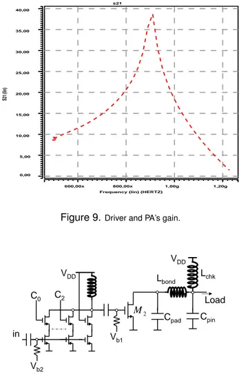
order to obtain eight different equally spaced voltage lev-els spanning the PA’s input range. Figure 9 shows the gain obtained with the driver in the highest gain (C0=C1=C2=1)
mode. The 1 dB compression point measured in this case is P1dB=8.1 dBm. S21 (lin) 0,00 5,00 10,00 15,00 20,00 25,00 30,00 35,00 40,00
Frequency (lin) (HERTZ)
600,00x 800,00x 1,00g 1,20g s21
Figure 9.Driver and PA’s gain.
2 M Vb1 C2 C0 Vb2 Load VDD VDD Cpad Cpin Lbond Lchk in
Figure 10.Power amplifier with controllable pre-amplifier.
Vr1 Vr3 Vr2 Vr4 Vm VLO VIF + -IRF- IRF+ VREF
Figure 11. Up-conversion mixer.
Figure 11 shows the up-conversion mixer. This mixer was adopted from [7] and modified in order to support both normal mission and test modes. In normal mission mode node Vm is connected to VREF allowing the two sides of
output current. Due to the differential operation the VLO
frequency component is suppressed in the mixer’s output. In test mode VIF is disconnected and Vm is pulled up to
VDD, leading the mixer’s right side to be off and the
out-put signal to be of constant amplitude at the LO frequency. A differential to single-ended signal converter provides the interface between the mixer output and the driver input.
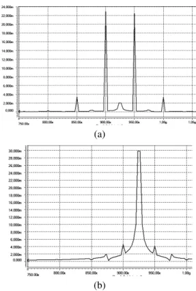
Figures ??.a) and ??.b) show the PA’s output spectrum, respectively, in normal mode and in test mode when a sin-gle tone signal is present at the VIFinput. In normal mode
two main frequencies at fLO±fIF are generated, while in
test mode one can see mainly a tone at fLO.
(a)
(b)
Figure 12.PA’s output spectrum: a) normal mode; b) test mode.
Using the proposed reconfigurable mixer the required extra circuitry overhead corresponds to a transmission gate used to switch-off the mixer’s VIF input plus the two
de-tectors. Their presence imply a degradation of about 1 dB in the gain seen between the VIFinput and the PA output.
The detectors (figure 13) to be placed at the PA’s in-put and outin-put (the driver’s gain is excluded in the test op-eration) allow to obtain the different voltage coordinates which define the PA’s input/output characteristic. The de-tectors’ characteristic shown in figure 13 show that a good measure linearity is ensured. That is a critical requirement in order that the PA’s characteristic linearity is not affected by the measures non-linearity.
4.2. Prototype simulation results
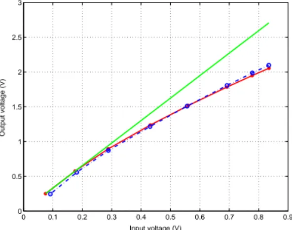
Figure 14 shows the voltage (rms values) transfer char-acteristics obtained observing the PA’s input and output voltages, respectively, the expected one (solid red line) and that obtained using the power detectors’ values (dashed
Vin Vout 0 0,5 1 1,5 2 2,5 3 0,2 0,4 0,6 0,8 1 1,2 1,4 1,6 1,8 2 2,2 2,4 vin VOUT VREF
Figure 13.Power detector.
blue line). One can see that the last one follows the ex-pected observed values with an error smaller than 0.1 dB. Figure 15 shows the respective power curves.
After finding the coefficients of the polynomials which define the two voltage curves one can compute the PA’s P1dB and IIP3 points using equations 5 and 6. Using the
directly observed voltages the values P1dB=7.2 dBm and
IIP3=16.8 dBm are obtained. These values are slightly dif-ferent from the ones mentioned above for the highest gain configuration, due to the non-linearity introduced by us-ing the different stages of the driver to generate the sweep. Using the values provided by the detectors one obtains P1dB=6.3 dBm and IIP3=16 dBm. The error due to using
these simple AC/DC converters as power detectors is thus about 1.0 dB. Values were also obtained affecting the ob-served voltages with a random noise. With a peak noise amplitude equal to 1% the maximum voltage, one obtains for P1dBa mean value of 6.5 dBm and a standard deviation
of 0.9 dBm. For the IIP3 these values are 16.1± 0.9 dBm. Increasing the peak noise amplitude to 3% the maximum voltage, one obtains P1dB=7.5± 3.7 dBm and IIP3=17.1 ±
3.8 dBm.
Concerning fault detection, taking the curve obtained with the detectors as a reference, it is also possible to know whether a fault is located in the PA or in the previous blocks, by mapping both input and output observed values with the reference ones. That is, if the observed input val-ues match the expected ones and those at the output do not, a fault is detected in the PA. If the observed input values do not match the expected ones the fault is occurring be-fore the PA. Placing more detectors allows to increase fault diagnosability.
5. Conclusions
A methodology is proposed which allows testing an embedded PA using a polynomial fitting characterization method. This method relies on applying a set of voltage values spanning the PA’s dynamic range and on capturing the respective output values. From this set of input/output values one can obtain the polynomial that best fits the PA’s transfer characteristic, whose coefficients allow one to cal-culate 1 dB compression and third order intercept point values. Simulated and experimental results have been
ob-0 0.1 0.2 0.3 0.4 0.5 0.6 0.7 0.8 0.9 0 0.5 1 1.5 2 2.5 3 Output voltage (V) Input voltage (V)
Figure 14. PA’s voltage transfer characteristic.
−100 −5 0 5 10 15 5 10 15 20 25 Output Power (dBm) Input Power (dBm)
Figure 15. PA’s power transfer characteristic.
tained which confirm the feasibility of this methodology to obtain accurate results for these parameters.
The BIST scheme being proposed to implement this method on-chip reuses the existing oscillator, up-conversion mixer, and PA’s driver to generate the differ-ent amplitude stimuli. Simple diode based AC/DC con-verters are used as peak voltage detectors at the PA’s in-put and outin-put. The up-conversion mixer is modified in order to allow applying a single-tone stimulus at the PA’s input, being the voltage sweep obtained using the scaling feature provided by the PA’s driver. This avoids including extra circuitry for stimuli generation and propagation. The only extra circuitry that is required is a transmission gate required to switch-off the mixer’s IF input and the two de-tectors. Simulation results show that a small performance degradation is obtained, and that parameters’ values can be obtained with an error of about 1 dBm. As the test opera-tion is controlled digitally and DC voltages are measured, no wide-bandwidth buses and specific instruments are re-quired to deal with delicate high frequency signals.
Acknowledgment
This work has been carried-out under the
frame-work of projects NanoTEST (2A702-MEDEA+,
www.lirmm.fr/∼w3mic/nanotest), and TARGET IST-1-507893-NOE (www.target-org.net). We are also grateful to Prof. H. Schumacher and Dr. C. Schick from the University of Ulm, for providing the facilities to conduct the measurements with the GaAs distributed amplifier.
References
[1] B. Cho, D. Thomas Kang, C.-H. Heng, and B. Sup Song. A 2.4-GHz Dual-mode 0.18-µm CMOS Transceiver for Blue-tooth and 802.11b. IEEE Journal of Solid-State Circuits, 39(11):1916–1926, November 2004.
[2] R. Green and J. Janesch. The importance of fast, economical testing for RFIC PAs, mobile phones. RF Design Magazine, pages 20–26, June 2004.
[3] A. Halder, S. Bhattacharya, G. Srinivasan, and A. Chatter-jee. A System-Level Alternate Test Approach for Spec-ification Test of RF Transceivers in Loopback Mode. In Proceedings of the IEEE 18th International Conference on VLSI Design held jointly with 4th International Conference on Embedded Systems Design (VLSID’05), pages 289–294, January 2005.
[4] M. M. Hella and M. Ismail. 2 GHz controllable power amplifier in standard CMOS process for short-range wire-less applications. IEE Proc.-Circuits Devices and Systems, 149(516):363–368, October/December 2002.
[5] M. S. Heutmaker and D. K. Lee. An Architecture for Self-Test of a Wireless Communication System Using Sampled IQ Modulation and Boundary Scan. IEEE Communications Magazine, pages 98–102, June 1999.
[6] M. H¨afele, A. Trasser, K. Beilenhoff, and H. Schumacher. A GaAs Distributed Amplifier With an Output Voltage of 8.5Vpp for 40Gb/s Modulators. In Gallium Arsenide ap-plications symposium. GAAS 2005, Paris, pages 345–348, October 2005.
[7] P. Kinget and M. Steyaert. A 1-GHz CMOS Up-Conversion Mixer. IEEE Journal of Solid-State Circuits, 32(3):370–376, March 1997.
[8] D. Lupea, U. Pursche, and H. J. Jentschel. Spectral Signa-ture Analysis - BIST for RF front-ends. Journal of Advances in Radio Science, 1:155–160, 2003.
[9] M. Negreiros, L. Carro, and A. A. Susin. Low Cost Analog Testing of RF Signal Paths. In Proceedings of the IEEE De-sign Automation and Test in Europe, pages 292–297, Febru-ary 2004.
[10] A. Rofougaran, G. Chang, J. Rael, J. Chang, M. Rofougaran, P. Chang, M. Djafari, M.-K. Ku, E. Roth, A. A. Abidi, and H. Samueli. A Single-Chip 900-MHz Spread-Spectrum Wireless Transceiver in 1-µm CMOS – Part I: Architecture and Transmitter Design. IEEE Journal od Solid-State Cir-cuits, 33(4):515–534, April 1998.
[11] J.-Y. Ryu, B. C. Kim, and I. Sylla. A New BIST Scheme for 5GHz Low Noise Amplifiers. In Proceedings of the Euro-pean Test Symposium (ETS’04), pages 127–132, May 2004. [12] G. Srinivasan, S. Bhattacharya, and A. Chatterjee. Fast specification test of TDMA power amplifiers using transient current measurements. IEE Proc.-Comput. Digit. Tech., 152(5):632–642, 2005.
[13] J.-H. Yoon, N. Ju-Y, K.-H. Lee, and S.-H. Son. A 900 MHz CMOS RF Power Amplifier with Digitally Control-lable Power. In IEEE International Conference on Com-puters, Communications, Control and Power Engineering (TENCON 2002), pages 1138–1141, October 2002.