Diogo Telmo Cruz Dias
Licenciado em Engenharia Electrotécnica e de Computadores
Transimpedance Amplifier for Early
Detection of Breast Cancer
Dissertação para obtenção do Grau de Mestre em Engenharia Electrotécnica e de Computadores
Orientador: Luís Augusto Bica Gomes de Oliveira,
Prof. Auxiliar, Universidade Nova de Lisboa
Júri:
Presidente: Prof. Doutor Pedro Miguel Ribeiro Pereira Arguente: Prof. Doutor Rui Manuel Leitão Santos Tavares
Vogal: Prof. Doutor João Pedro Abreu de Oliveira Setembro, 2014
iii
Transimpedance Amplifier for Early Detection of Breast Cancer
Copyright © Diogo Telmo Cruz Dias, Faculdade de Ciências e Tecnologia, Universidade Nova de Lisboa.
A Faculdade de Ciências e Tecnologia e a Universidade Nova de Lisboa têm o direito, perpétuo e sem limites geográficos, de arquivar e publicar esta dissertação através de exemplares impressos reproduzidos em papel ou de forma digital, ou por qualquer outro meio conhecido ou que venha a ser inventado, e de a divulgar através de repositórios científicos e de admitir a sua cópia e distribuição com objectivos educacionais ou de investigação, não comerciais, desde que seja dado crédito ao autor e editor.
v The work presented in this thesis was only made possible given the motivating environment found in the Department of Electrical Engineering of the Faculty of Sciences and Technology. For that, for providing the means necessary to the development of this work and for the high institutional standards presented, I would like to address a truthful and deep word of appreciation.
I would also like to thank Professor Luís Oliveira, my thesis advisor, for the relentless support, patience, dedication and availability demonstrated. Without any of these characteristics, this work would have had become an exponentially harder feat to achieve, if achieved at all. I would still like to mention that the trust he placed upon me have been crucial to the good conclusion of this work. For all the mentioned, a sincere and ever unforgettable word of gratitude.
To Professor João Goes and Professor João Pedro Oliveira, I would like to address a special appreciation for their support and interest demonstrated. Their motivational capability has kept me in the right track countless times. To Professor Rui Tavares, I would like to issue a word of appreciation regarding all the support provided with some technical issues that came by. I would still like to address a very sincere and strong word of gratitude to Professor Manuel de Medeiros Silva. His lectures and monitoring, in an early stage of my academic path, have been the main driver for pursuing a specialization in electronics and, even though not being physically present, his influence will always be an intellectual reference to me.
To all my office colleagues – Nuno Pereira, Diogo Inácio, Miguel Fernandes, Filipe Melo and João Eusébio – I can only wish the best academic success. Thank you for the technical help and suggestions, fun times and for providing a wonderful working environment. To my non-office colleagues – Pedro Sardinha, Carlos Gaspar, Raúl Guilherme, Diogo Sousa and Hugo Serra – a deep appreciation for the good times spent and for making me feel at home day after day.
Finally, for my better half, Marisa Esteves, I can undoubtedly state that without her none of this would have been made possible. My gratitude to her, for sticking with me in these last five, difficult, years is eternal. For being my safe haven, that kept me strong, when everything else crumbled, for being an immense inspirational and motivational source, for all that she has lost while helping me find myself and for her unconditional support, I am eternally grateful. No matter what, this will always be present in me. Thank you, without you I could never be where I am today.
vii
Resumo
Faculdade de Ciências e Tecnologia
Departamento de Engenharia Electrotécnica e de Computadores
Dissertação para obtenção do grau de Mestre em Engenharia Electrotécnica e de Computadores
por Diogo Telmo Cruz Dias
O cancro da mama é o tipo de cancro mais comum, à escala mundial. A eficácia do seu tratamento depende, não só, de uma detecção atempada, mas também da precisão do seu diagnóstico. Algumas técnicas de diagnóstico como a Ressonância Magnética, Sonogramas por Ultra-som e Tomografia por Emissão de Positrões (PET) têm sofrido avanços consideráveis. O trabalho aqui apresentado incide sobre o estudo de uma aplicação PET direccionada para a Mamografia por Emissão de Positrões (PEM).
Um sistema PET/PEM opera sob o princípio no qual um cristal cintilante deverá detectar um impulso de raios gama, originado nas células cancerígenas, convertendo-o num impulso de luz visível. Este último deverá ser convertido num impulso de corrente eléctrica através de um Dispositivo Fotossensível (PSD). Após o PSD, surge um Amplificador de Transimpedância (TIA), cujo objectivo é o de converter o impulso de corrente numa tensão de saída num período de tempo inferior a 40 ns.
No trabalho aqui apresentado é considerado um Fotomultiplicador de Silício (SiPM). A utilização deste dispositivo é impraticável com as topologias de TIAs convencionais. Logo, o projecto do amplificador será sujeito à utilização da topologia Porta Comum Regulada (RCG). Serão apresentadas duas variações da referida topologia, consistindo numa melhoria da resposta do ruído e possibilidade de operação em modo diferencial. A referida topologia irá ainda ser testada no contexto de um receptor de Radiofrequência. Será também apresentado um estudo que incluirá um TIA com realimentação auto-polarizado em tensão reduzida.
Os circuitos propostos são simulados com tecnologia CMOS padrão (UMC 130 nm), alimentados a 1.2 V. Obteve-se um consumo de potência de 0.34 mW e uma relação sinal-ruído de 43 dB.
Palavras-Chave: Tomografia por Emissão de Positrões, Detectores de Radiação, Amplificador de
ix
Abstract
Faculdade de Ciências e Tecnologia
Departamento de Engenharia Electrotécnica e de Computadores
Dissertação para obtenção do grau de Mestre em Engenharia Electrotécnica e de Computadores
por Diogo Telmo Cruz Dias
Breast cancer is the most common type of cancer worldwide. The effectiveness of its treatment depends on early stage detection, as well as on the accuracy of its diagnosis. Recently, diagnosis techniques have been submitted to relevant breakthroughs with the upcoming of Magnetic Resonance Imaging, Ultrasound Sonograms and Positron Emission Tomography (PET) scans, among others. The work presented here is focused on studying the application of a PET system to a Positron Emission Mammography (PEM) system.
A PET/PEM system works under the principle that a scintillating crystal will detect a gamma-ray pulse, originated at the cancerous cells, converting it into a correspondent visible light pulse. The latter must then be converted into an electrical current pulse by means of a Photo- -Sensitive Device (PSD). After the PSD there must be a Transimpedance Amplifier (TIA) in order to convert the current pulse into a suitable output voltage, in a time period lower than 40 ns.
In this Thesis, the PSD considered is a Silicon Photo-Multiplier (SiPM). The usage of this recently developed type of PSD is impracticable with the conventional TIA topologies, as it will be proven. Therefore, the usage of the Regulated Common-Gate (RCG) topology will be studied in the design of the amplifier. There will be also presented two RCG variations, comprising a noise response improvement and differential operation of the circuit. The mentioned topology will also be tested in a Radio-Frequency front-end, showing the versatility of the RCG. A study comprising a low-voltage self-biasing feedback TIA will also be shown.
The proposed circuits will be simulated with standard CMOS technology (UMC 130 nm), using a 1.2 V power supply. A power consumption of 0.34 mW with a signal-to-noise ratio of 43 dB was achieved.
Keywords: Positron Emission Tomography, Radiation Detectors, Transimpedance Amplifiers,
xi
Acknowledgements ... v
Resumo ... vii
Abstract ... ix
List of Figures ... xiii
List of Tables ... xv
Acronyms and Abbreviations ... xvii
1 1. Introduction ... 1 .
1.1. Background and Motivation ... 1
1.2. Objectives ... 2
1.3. Thesis Structure and Organization ... 4
1.4. Main Contributions ... 6
2 2. PET Systems and Radiation Detectors ... 7 .
2.1. PET System Physical Principles ... 7
2.1.1. Positron Annihilation ... 8
2.1.2. Photon Detection ... 9
2.2. System Requirements ... 12
2.2.1. Radiation Detector Front-end ... 12
2.2.2. RF Receiver Front-end ... 14
2.3. Basic Amplification Topologies ... 16
2.3.1. Common-Source Voltage Amplifier ... 17
2.3.2. Common-Gate Voltage Amplifier ... 22
2.3.3. Common-Gate Transimpedance Amplifier ... 25
xii
3.1. Basic Regulated Common-Gate TIA ... 36
3.2. Improved Noise Distribution ... 43
3.3. Differential Output RCG TIA ... 48
4 4. TIA Sizing and Design Procedures ... 55.
4.1. RCG TIA in a RF Receiver Front-end ... 56
4.2. RCG TIA in a Radiation Detector Front-end ... 59
4.2.1. Basic RCG TIA ... 60
4.2.2. RCG TIA with Noise Improvement ... 62
4.2.3. RCG TIA with Differential Output ... 64
5 5. Simulation Results ... 69 .
5.1. Radiation Detector Front-end Results ... 69
5.2. Design of a Low-voltage Feedback TIA With an APD at the Input ... 78
5.3. Results Comparison and Final Remarks ... 80
6 6. Conclusions and Future Work ... 83.
References ... 87
Appendix A Miller’s Theorem ... 91
Appendix B RF Receiver Front-end Simulation Results ... 93
Appendix C Internal Report ... 97
Appendix D Published Papers ... 105
xiii
Figure 1.1 - Representation of a PET/PEM patient interface (adaptation from [10]). ... 2
Figure 1.2 - Block diagram of the PET/PEM front-end. ... 3
Figure 2.1 – Illustration of the annihilation process (adaptation of [18]). ... 9
Figure 2.2 – Generalized gamma ray detection using spatial resolution. ... 10
Figure 2.3 – Image of a 256 LYSO crystal matrix and various 16 LYSO crystal matrixes (adapted from [23]). ... 10
Figure 2.4 – Constituting blocks of a photon detector with a scintillating crystal and a PSD (adapted from [18]). ... 11
Figure 2.5- Image of both types of PSDs: a) 32 APDs matrix [27]; b) 16 SiPMs matrix [28]. ... 12
Figure 2.6 – Generalized architecture of a radiation detector front-end with the TIA’s input current, , and output voltage, , shapes (adapted from [8]). ... 12
Figure 2.7 – Block diagram of a heterodyne receiver architecture with focus on the mixer and TIA. ... 14
Figure 2.8 – Block diagram of a mixer. ... 14
Figure 2.9 – Example of frequency down-conversion in heterodyne receivers. ... 15
Figure 2.10 – Schematic of a basic mixer with its equivalent output capacitance and TIA’s equivalent input impedance. ... 16
Figure 2.11 – Common-source configuration with: a) passive load; b) active load. ... 17
Figure 2.12 – Graphical analysis of CS configuration (adapted from [31]). ... 18
Figure 2.13 – Low frequency incremental model of the CS configuration. ... 18
Figure 2.14 – Incremental CS model with respective noise sources. ... 19
Figure 2.15 – High frequency model of the CS configuration. ... 20
Figure 2.16 – Common-Gate configuration with: a) passive load; b) active load. ... 22
Figure 2.17 – Low frequency incremental model of the CG configuration. ... 22
Figure 2.18 – Incremental CG model with respective noise sources. ... 23
Figure 2.19 – High frequency incremental model of the CG configuration. ... 24
Figure 2.20 – Simplified model for the high frequency CG stage. ... 25
Figure 2.21 – Schematic of the CG TIA topology. ... 26
Figure 2.22 – Incremental model of the CG TIA. ... 26
Figure 2.23 – Incremental model of the CG TIA with its thermal noise contributors... 28
Figure 2.24 – Feedback TIA Basic configuration. ... 30
Figure 2.25 – Equivalency between the OpAmp’s input stage thermal noise contribution. ... 32
Figure 2.26 – Feedback TIA with its thermal noise voltage source. ... 32
Figure 3.1 – Schematic of the basic RCG TIA circuit. ... 36
xiv
Figure 3.5 – M3’s configuration incremental model. ... 45
Figure 3.6 – RCG TIA incremental model with M3’s configuration equivalent impedance, Z3. .. 46
Figure 3.7 – Proposed differential output RCG TIA... 48
Figure 3.8 – Partial incremental circuit of the inverted output. ... 49
Figure 3.9 – Partial incremental circuit of the inverted output with M2’s thermal noise contribution. ... 51
Figure 4.1 – Basic RCG TIA with parasitic capacity CX and a low-pass functional block, H(s). . 57
Figure 4.2 – RCG TIA with biasing current sources sizing. ... 59
Figure 4.3 – Sizing of the basic RCG TIA with a SiPM at the input. ... 62
Figure 4.4 – Sizing of the RCG TIA with improved noise response, with a SiPM at the input. ... 63
Figure 4.5 – Schematic of the differential RCG TIA with output buffer included. ... 64
Figure 4.6 – Complete schematic of the proposed version of the differential RCG TIA with output buffer. ... 66
Figure 5.1 – Output voltage in: a) Basic RCG TIA; b) RCG TIA with improved noise response. 70 Figure 5.2 – Differential RCG TIA output: a) TIA core output signal; b) Output buffer output signal. ... 71
Figure 5.3 – M2’s frequency response with dominant pole: a) Basic RCG; b)RCG with noise improvement; c) differential version. ... 71
Figure 5.4 – TIAs’ output frequency response. ... 72
Figure 5.5 – Phase and magnitude Bode diagrams: a) Basic RCG; b) RCG with improved noise; c) Differential RCG. ... 73
Figure 5.6 – Linearity for each circuit designed: a) Basic RCG; b) RCG with improved noise; c) Differential RCG. ... 73
Figure 5.7 – Noise response of the TIAs with a SiPM... 74
Figure 5.8 – Differential RCG TIA 27 corners output voltage. ... 75
Figure 5.9 – Corner analysis for the differential transimpedance gain. ... 76
Figure 5.10 – Phase and magnitude Bode diagrams for all the 27 corners. ... 76
Figure 5.11 – Detail of the physical layout of the differential version of the RCG TIA ... 77
Figure 5.12 – Two-stage inverter-based self-biased CMOS amplifier. ... 79
xv Table 4.1 – MOS devices parameters with the mixer at the input; VOdc = 0.6 V, RX = 200 kΩ... 59
Table 4.2 – MOS devices parameters for the basic RCG TIA with a SiPM at the input. VOdc = 0.5
V; tm = 36 ns; RX = 23.2 kΩ. ... 62
Table 4.3 – MOS devices parameters for the RCG TIA with improved noise response, with a SiPM at the input. VOdc = 0.5 V; tm = 36 ns; RX = 23.2 kΩ. ... 63
Table 4.4 – MOS devices parameters for the differential RCG TIA proposed, with a SiPM at the input. RX1 = RX2 = 20 kΩ; VO1dc = VO2dc = 0.6 V; VOPdc = VONdc = 0.3V; tmdiff = 38 ns.
... 67 Table 5.1 – Low frequency gain, time-constant τa and its pole frequency for the three circuits. ... 72
Table 5.2 – Low frequency transimpedance gain, time-constant τp and its pole frequency for the
three circuits. ... 72 Table 5.3 – Top five noise contributors in the three RCG TIAs, designed to operate with a SiPM at the input. ... 75 Table 5.4 – TIA comparison. ... 81
xvii
MRI Magnetic Resonance Imaging
PET Positron Emission Tomography
PEM Positron Emission Mammography
PSD Photo-Sensitive Device
APD Avalanche Photo-Diode
SiPM Silicon Photo-Multiplier
TIA Transimpedance Amplifier
ASIC Application Specific Integrated Circuit
CG Common-Gate
RCG Regulated Common-Gate
OTA Operational Transconductance Amplifier
SNR Signal-to-Noise Ratio
TF Transfer Function
NTF Noise Transfer Function
RF Radio Frequency
MOS Metal-Oxide Semiconductor
FET Field Effect Transistor
FDG 2-deoxi-2-[18F]fluoro-d-glucose (fluorodeoxyglucose)
LYSO Lutetium-Yttrium Oxyorthosilicate
LO Local Oscillator
RF IN Radio Frequency Input
IF OUT Intermediate Frequency Output
LPF Low-Pass Filter
CS Common-Source
xviii
KCL Kirchhoff Current Law
LNA Low-Noise Amplifier
NF Noise Figure
VCVS Voltage-Controled Voltage Source
CD Common-Drain
PVT Process, Voltage and Temperature
FOM Figure-of-Merit
CMFB Common-Mode Feedback
1
1
1
.
.
INTRODUCTION
1.1.
B
ACKGROUND AND
M
OTIVATION
reast cancer has been the most common type of cancer worldwide [1]. As in any type of cancer, it is of paramount importance to take measures, which reduce the disease’s impact as soon as detection occurs. An early diagnosis can most times allow for preemptive options and treatment, made impossible with late-stage detection. This latter topic, early breast cancer detection, is the main driver for the work here presented. For that matter, specialists in the field have been making use of medical imaging techniques such as x-ray mammography (mammograms), almost since radiographies started giving their contribute as a diagnosis tool. However, the limitations of this method can originate false positive and false negative results, over-diagnosing and over-treatment, difficulty in obtaining a good image in patients with breast implants and patient discomfort during the exam [2], [3]. To overcome these limitations, in the last decade researchers have been trying to develop innovative medical imaging systems achieving more precise, better quality and higher image resolution systems. Therefore, a new range of powerful and useful diagnosis instruments [4], [5], [6] which become very effective when working in tandem, have been originated. Diagnosis techniques have been submitted to relevant breakthroughs since the upcoming of Magnetic Resonance Imaging (MRI), Ultrasound imaging (e.g. sonograms) and Positron Emission Tomography (PET) scans, among others. With these techniques, new types of analysis became preponderant since it permitted for different functional and behavioral testing of the areas and organs under study.
The work presented here is focused on studying the application of a PET system to a Positron Emission Mammography (PEM) system, responsible for early detection of breast cancer. A PET system works under the principle that the patient will be injected with a safe dose of radioactive material, often called radiotracer, which will be concentrated around the area under study, as can be seen in Fig. 1.1. Contrarily to x-ray imaging, PET technology monitors the rate of metabolism or chemical activity present in a given area, giving a more behavioral analysis of the organs under study instead of a physiognomic one. When a particle of the radiotracer becomes
2
consumed it will emit two -ray bursts, which can be detected by a scintillating crystal matrix which, in turn, will produce a corresponding light pulse. Afterwards, this light pulse can be converted into a current pulse by means of a photodiode [3], [7], [8]. At present, there are two mainstream options regarding the detection of the -rays using photodiodes, both accomplished by means of a Photo-sensitive Device (PSD). The first, and older, uses an Avalanche Photo-diode (APD) matrix. The remaining, more recently developed [9], is accomplished with the usage of a Silicon Photo-Multiplier (SiPM) matrix. The latter option (SiPM) is capable of reaching higher output peak currents, but its output equivalent capacity is also higher. In conceptual terms it can be understood that for each option, different development methodologies must be adopted, depending on the type of device used. While with an APD the most common and traditional methodologies can be used, with a SiPM some topologies may be impracticable due to its higher output capacity. Radiotracer Crystal matrix PSD PSD Gamma rays
Figure 1.1 - Representation of a PET/PEM patient interface (adaptation from [10]).
1.2.
O
BJECTIVES
iven the different options regarding the choice of PSDs it is important to establish and set not only the limits where an APD or a SiPM may be used, but the system’s development methodologies for each PSD as well. In any case, since both types produce an output current as a function of the radiation received, it is necessary to convert the first into a suitable voltage, with the desired shape and amplitude, for further processing [10], as it is shown in Fig. 1.2. This conversion can be accomplished via a Transimpedance Amplifier (TIA), with different
3
topologies, depending on the type of PSD used. A TIA is a device commonly used in applications, which require current-voltage conversion and signal shaping. TIAs are widely applied in nuclear science, instrumentation and medical imaging [9], [11], which is the main focus of this thesis. Moreover, this type of devices are also used in RF front-ends and optical communications systems [12], [13], [14], The type of TIAs here designed are widely used in PET scanners front-end. As an example, in [10] a total of - channel Application-Specific Integrated Circuits (ASICs) were developed, where the most challenging part of it was the design of the 192 TIAs with the respective APDs at their inputs, since the first is what determines the system’s limits of performance. The main focus of the work presented here is to develop the front-end of a PEM scan system using a SiPM as an input device. The TIA developed should not exceed a power consumption of 1 mW, while being able to present the capability of pulse shaping and maintaining low noise level.
TIA Buffer & Post--amplifier
TIA Buffer & Post--amplifier Front-end id id vo vTIA vTIA vo ADC ADC D a ta A q u is iti o n a n d d ig ita l p ro c e s s in g n-channels n-channels
Gamma ray Crystal
matrix PSDs
Figure 1.2 - Block diagram of the PET/PEM front -end.
The classical approach is to design the front-end using a Feedback TIA based on capacitive noise matching [14], where the input capacity of the TIA would match the PSD’s output capacity. However, with the SiPM at the input, not only this topology becomes impracticable, mainly due to the SiPM’s high output equivalent capacity, but also the output voltage rising time would be too high for the application it is designed for. Therefore, alternative topologies must be taken into account. In order to support this fact, a study and an extensive evaluation of the three most used topologies will be made. The choice of topologies studied will fall into the feedback-TIA, the Common-Gate (CG) TIA and, finally, the Regulated Common-Gate (RCG) TIA. As an improvement of the CG TIA, the RCG TIA will be more extensively studied than its counterparts, since it will be the topology of choice. In order to prove the impracticability of the feedback TIA with the SiPM at the input, a study will be presented considering the design of a PEM scanner
4
front-end using the referred topology with an APD and a SiPM. For the effect, a previously studied and developed Operational Transconductance Amplifier (OTA) will be used.
During the study of the RCG TIA various development phases are to be encountered in the progress of this dissertation. In a first phase a study of the basic topology will be made concerning a conceptual and functional analysis. In the second phase the basic RCG TIA will be slightly altered in order to achieve a better overall device noise distribution, presenting slightly improved noise level and signal-to-noise ratio (SNR). Finally, in the last phase, the possibility of differential output will be considered, further exploring the development taken by in the second phase, improving the TIA’s output voltage amplitude. For any of these phases, there will be a detailed analysis contemplating the TIA’s transfer function, or Transimpedance Function (TF), the Noise Transfer Function (NTF) with its pole-zero location, circuit’s linearity and output voltage amplitude and shape. In addition, the RCG TIA will also be considered in a Radio-Frequency (RF) receiver, providing there is a hypothetical generalized passive mixer at the input, showing this topology’s versatility and adaptability.
The main focus of this dissertation is to provide the guidelines necessary to design a RCG TIA meant to operate with a SiPM at the input, explore any range of options that can permit a noise reduction of the front-end system, provide proof that with the PSD chosen the more traditional solutions cannot be considered, show the versatility of this topology in the context of a RF front-end and, finally, design and simulate the circuits in a standard CMOS 130 nm technology.
1.3.
T
HESIS
S
TRUCTURE AND
O
RGANIZATION
n the present section the interest remains in showing the key topics discussed in this dissertation and provide a guide to the structure adopted. Accounting for the present introductory chapter, the work here presented will be sectioned into six main chapters which describe the basic knowledge into the state of the art regarding PET systems, radiation detectors, some insight into Metal-Oxide Semiconductor (MOS) Field-Effect Transistors (FETs), TIA topologies, and the chosen circuit’s analysis, development and evaluation. In a more detailed description, one will find the following chapters:
Chapter 2 – PET Systems and Radiation Detectors
In this chapter it is intended to review the state of the art regarding PET systems and present some considerations regarding a hypothetical passive mixer, making the TIA operate in a RF context. Some PET considerations such as the physical principles behind this technology,
5
system’s requirements and specifications along with some insight into PSDs will be contemplated. Regarding the passive mixer, a brief definition will be given providing the specifications used in the design of the TIA for that matter. In the last part of this chapter, high focus will be given in providing a study of some of the topologies most commonly used and the principles in circuit design with MOS devices and amplification stages used. There will be a distinction between three major topics, with these being a study of the MOS device and amplification stages necessary, the feedback TIA and the CG TIA.
Chapter 3 – The Regulated Common-Gate Transimpedance Amplifier
In the third chapter the focus is to study the referred TIA topology. For each phase of development there will be a sub-chapter contemplating a conceptual and behavioral analysis of the circuit. The interest here remains in showing a circuit description, transimpedance function and noise transfer function in a succinct and objective manner. The three sub-chapters will be distinguished by the differences in the circuits’ schematics, which will correspond to the basic RCG, the RCG with improved noise distribution and, finally, with differential output.
Chapter 4 – TIA Sizing and Design Procedures
This chapter will have the purpose of showing the options taken in the design of the circuits. For each development phase, the sizing of the TIAs will be shown and commented. The chapter will be divided into two sections, in which the design of the TIA in a RF front-end context and, separately, by each development stage, in a Radiation Detector front-end context, will be studied.
Chapter 5 – Simulation Results
The obtained results will be shown and compared in this chapter in order to provide an idea of which choices prove to be better. Separately, the design of a feedback TIA with an APD at its input will be shown and properly analyzed. In this chapter only the main results from the RCG TIA designed to operate with a passive mixer at the input will be shown, proving the versatility of this topology.
Chapter 6 – Conclusions and Future Work
In the last chapter, final remarks and considerations will be made, comprising a conclusion of the work taken by herein and possible future development and research topics referent to the work presented.
6
1.4.
M
AIN
C
ONTRIBUTIONS
egarding any scientific contributions, it is of best hope that the work presented may serve as a guideline to the implementation of PEM scan systems front-end, using the most recently developed SiPM technology. It is also of best hope that the circuit’s versatility can be taken into account, given the RF receiver context. With the improved noise distribution and low power consumption, it is expectable that this dissertation will present a viable solution for the next generation of ASICs in the area of PEM medical imaging.
Some of the work presented here contributed with a publication accepted for oral presentation at 2014 IEEE International Conference Mixed Design of Integrated Circuits and Systems (MIXDES) [15]. Recently, this paper originated an invite of an extended version to be submitted into the International Journal of Microelectronics and Computer Science.
7
2
2
.
.
PET SYSTEMS AND
RADIATION DETECTORS
n this chapter PET/PEM systems basics for radiation detectors will be reviewed. Some aspects and concepts of these systems will be succinctly exposed, such as the radiotracer used, physical principles behind tumor detection, radiotracer annihilation and photon detection. Thus, the system requirements for the design here taken by will be given. Finally, the RF front-end along with its mixer will be shown in order to give a certain level of contextualization. In the last part of the chapter some of the topologies most commonly used, along with the amplifying stages that constitute them, will be studied.
2.1.
PET
S
YSTEM
P
HYSICAL
P
RINCIPLES
ositron emission, or decay, is the process by which an atom obtains the optimal ratio between its protons and neutrons [16], [17]. Basically, it reflects a common method where an atom has one of its protons converted into a neutron and a positron. A positron, commonly known as an anti-electron, is the anti-particle of the electron. Both particles have same mass but opposite electrical charge. When a positron is ejected from the nucleus of an atom the energy originated can vary from zero to a maximum emission energy, [18]. In a PET system this is the key
principle behind this imaging technique. The first step in the realization of a PET exam is the injection of the radiotracer responsible for the positron emission into the subject under study [19]. Basically, a radiotracer is a chemical compound, in which, one or more of its atoms have been replaced by a radioisotope. In PET technologies the radiotracer most commonly used is the 2-deoxi-2-[18F]fluoro-d-glucose, also known as fluorodeoxyglucose (FDG), which stands for a molecule similar to glucose that is absorbed by the cells using its same transport method. After being absorbed the FDG is phosphorylated and, since the resultant compound cannot be metabolized, it will remain in the cell where it was absorbed being, this way, able to serve as a marker in the metabolic rate of glucose [18]. Cancer cells have a glucose consumption far more
I
8
superior then healthy tissue, making it possible to differentiate the types of tissues being observed [20]. This is where PET scans differ from other imaging techniques such as x-ray imaging. By quantitatively observe the metabolic rate of glucose consumption, this technique offers a functional or metabolic analysis of the areas under study, instead of an anatomic analysis.
2.1.1. Positron Annihilation
uman tissue is a highly rich environment in electron density. Logically, this means that the ejected positron will be quickly consumed, resulting in a very short lifetime period. Most of its kinetic energy will be promptly dissipated by interacting with other electrons present in the human tissue. Having most of its energy dissipated, the positron can then be combined with an electron, in a hydrogen-like state, often called positronic, that will last for only around 10-10 seconds. Following this period of time, a process known as annihilation will occur where the masses of both the electron and the positron will be converted into electromagnetic energy. By practically being at rest, this conversion of mass into energy will be due to the particles masses. One can have the resultant energy measured through Einstein’s equation [18]:
(2.1)
where are the masses of the electron and positron and is the light speed in vacuum. The energy originated by the annihilation will result in a total of , which is the same as approximately [21].
When annihilation occurs the electron-positron pair is practically at rest, which means that the resultant linear momentum is near zero. The energy originated at the annihilation will be released in the form of high energy photons and, given the linear momentum, spin and energy conservation laws [19], the process will result in the emission of two equal high energy photons, expelled in opposite directions. Note that otherwise – if a single photon was expelled or photons direction was not opposite – the conservation of the linear momentum would not be verified, since it would have the resultant direction. The energy originated will be equally divided by both photons which means that each one will be presenting an energy of 511 keV which, regarding the electromagnetic spectrum, characterizes these photons in the gamma ray range. Fig. 2.1 illustrates the behavior of the electron-positron pair in the referred process.
9 Nucleus β+ decay e+ e -Ephoton = 511 keV Ephoton = 511 keV n p+
Figure 2.1 – Illustration of the annihilation process (adaptation of [18]).
The annihilation photons, or gamma ray photons, are highly energetic and, therefore, they can be detected after working their way out of the human body [21], [18]. Contrarily to what the system’s name suggests, it is the gamma ray photons that can be detected instead of the positrons, since these latter ones collapse inside the human body. One other point worth mentioning is the fact that since the gamma ray photons are expelled with a very high geometrical precision, the line that is common to both detection points, called line of response, will pass directly through the point of annihilation [18]. By measuring the total amount of radiation, obtained by several lines of response, it is then possible to reconstruct an image of all the points where annihilation has been detected via computerized, mathematical algorithms, even though this is an aspect out of the scope of this thesis.
2.1.2. Photon Detection
ne of the most important specifications in a PET system is the minimum resolution to which the system can capture and reproduce an image. A system with a good minimum resolution will be able to identify smaller masses, becoming a more precise system. The system’s resolution can be defined as the minimum detectable distance between two points in an image [22]. In order to detect the incident photons, two major techniques are employed: the first uses timing resolution, in which annihilation positioning is accomplished through the timing differences between the arrival of each annihilation photon [18]; the second method – the one of interest in the present work – uses spatial resolution which, basically, is accomplished by using two matrixes of detectors as shown in Fig. 2.2.
10 Crystal matrix Tumor Human tissue Radiotracer Gamma ray
Figure 2.2 – Generalized gamma ray detection using spatial resolution.
Photon detectors are usually accomplished by means of a scintillating crystal. There is a wide range of crystal types for that matter but, the ones we are interested in are Lutetium-Yttrium Oxyorthosilicate (LYSO) crystals. These innorganic crystals, usually transparent, have a higher density than most, making it possible to accomplish higher precision in photon detection. They are characterized by their stopping power, light emission wavelenght and duration of light pulse, or decay time [18]. Usually, in a LYSO crystal, the decay time is around 40 nanoseconds. A scintillating crystal has the purpose of serving as an interaction media between the gamma rays it receives and the visible light photons it emmits. In Fig. 2.3 some examples of LYSO crystal matrixes can be found.
Figure 2.3 – Image of a 256 LYSO crystal matrix and various 16 LYSO crystal matrixes (adapted from [23]).
When a scintillating crystal receives a high energy photon such as a gamma ray, it will isotropically emmit visible light, proportional to the energy received as can be seen in Fig. 2.4. Immediately after the scintillating crystal there must be coupled a PSD such as a photodiode responsible for the conversion of the light pulse, originated in the crystal, into a correspondant electrical current. The current produced at the PSDs output will be proportional to the amount of light it received and, therefore it will be proportional to the energy contained in the gamma ray detected by the LYSO cristal.
11 PSD Output current pulse LYSO crystal 511 keV photon
Figure 2.4 – Constituting blocks of a photon detector with a scintillating crystal and a PSD (adapted from [18]).
Regarding PSDs, these are devices that, by taking advantage of the photoelectric effect, are able to convert visible light into an electrical current. In a PET system, the most commonly adopted solution is to use an APD coupled with the scintillating crystal. In the electronics front-end the PSD can be considered the first stage to provide gain to the signal. Therefore, one must take into account that the higher the gain presented by the PSD, the higher the SNR will be [24]. These devices can be characterized by a few basic parameters such as quantum efficiency, excess noise factor, dark or output peak current, , output capacitance, , and operating voltage. However, for the sake of the present work we are only interested in these devices’ output current and capacity.
One other type of a PSD, the one considered here, is the most recently developed SiPM. This type of device is built in arrays of Geiger-mode APDs with resistive quenching, connected in parallel on common silica substrate and has the ability of single-photon detection in a time response much lower than 1 nanosecond [9]. One of the properties that makes this type of device a suitable candidate for PET imaging systems is its low operating voltage capability, ranging from 20 to 100 V, depending on the APD technology used. As with APD technology, regarding SiPMs we are interested in accounting for the output current and capacitance values. These parameters, for the referred devices, are and for the APD; and and with a SiPM. Note that in the case of the SiPM the output capacitance may vary from 100 – 300 pF [7] but, in any case, we tend to use the worst case scenario value (higher output capacitance). By having a higher output current, one could be led to think the SiPM would necessarily bring a higher output peak voltage. However, due to its higher output capacitance, it becomes difficult to accomplish an output voltage that has a suitable shape, without increasing the power consumption beyond the acceptable. This is the main reason why alternative solutions must be found when designing the TIA with a SiPM at the input.
In this work the interest remains in the analysis of the electronics front-end of the system. Therefore, regarding PSDs, it is important to reveal their equivalent electrical circuit. For both PSD cases – in the case of a SiPM, a simplified version [9] – their equivalent circuit is a current source, , in parallel with the equivalent output capacitance, [25], [26]. In Fig. 2.5 an example of a matrix with both PSDs is presented.
12
Figure 2.5- Image of both types of PSDs: a) 32 APDs matrix [27]; b) 16 SiPMs matrix [28].
2.2.
S
YSTEM
R
EQUIREMENTS
uch like any other type of system, the PET/PEM front-end must fulfill a given number of requirements. In the present sub-chapter, these will be described. Concepts such as input current and output voltage shape, rising or peaking time, SNR, power consumption, supply voltage and integrated noise level will be mentioned. As another point of interest, a contextualization regarding the TIA in a RF front-end, with a passive mixer at the input will be provided.
2.2.1. Radiation Detector Front-end
ollowing what was previously stated, the TIA must be inserted into the front-end shown in Fig. 1.2 with the objective of converting any type of PSD’s output current into a suitable voltage, i.e., its input current pulse must be transformed into a voltage pulse with the desired shape and amplitude. Fig. 2.6 shows the equivalent circuit of any of the PSDs here mentioned (a simplified model in the case of a SiPM) coupled with a basic transimpedance block, along with the TIA’s input current and output voltage shapes.
𝜏 ( ) 𝑉 ( ) 0 100 ns id Cd TIA vO PSD
Figure 2.6 – Generalized architecture of a radiation detector front -end with the TIA’s input current, , and output voltage, , shapes (adapted from [8]).
M
13
The input current pulse, , has a very fast rising time (much lower than one nanosecond in the case of the SiPM [9]) and, after reaching its maximum peak current, , it starts decaying
following a time-constant 𝜏 [15], following
(2.2)
This time-constant is dependent on the technology used in order to achieve the PSD and, with the LYSO technology chosen, it is approximately 𝜏 . The output voltage must be as the one shown in Fig. 2.6. Even though the exact shape of is not of paramount importance, its variation must reach a maximum peak voltage, 𝑉 , in less than forty nanoseconds, which means
. This peaking time is a key restriction since the work here presented is based in previous studies [10] and, will limit the performance of the system’s front-end, as it will be seen further on. In the sizing presented was aimed to be lower than the required in order to contemplate the expectable high parasitic capacitances in the output buffer which, most definitely, will influence the TIA’s frequency response. One requirement that must be fulfilled at any cost is a good and predictable linearity between and 𝑉 , i.e., the total charge injected by the current
source, , in which
𝜏 (2.3)
must be proportional to 𝑉 , without affecting the peaking time. In practical terms this will
impose that the amplifier’s input and output must have a linear relation.
Since the work here presented is based in previous studies, the requirements necessary to accomplish a good design follow the ones in [7], [8], [10]. Therefore, following these latter ones, the transimpedance function must have two poles in order to accomplish the desired pulse shaping, having the form:
𝑉
𝜏 𝜏 (2.4)
where denotes the low frequency transimpedance gain of the amplifier. Actually, a single-pole system would suffice in order to obtain the pulse shaping required. The problem with such an approach is that since the noise transfer function will have a low frequency zero – as it will be seen in the following chapters – the transimpedance function must have one other pole so it can cancel the mentioned zero. It is also estimated that the output peak voltage must reach 𝑉 ,
14
characterization of the design here submitted, 𝑉 , it becomes impossible to reach the
desired output peak voltage and, since this is a mandatory requirement, a post-voltage amplifier must be used after the output buffer. This way, the output voltage can reach the required value maintaining approximately the same SNR value. Following the requirements stated, it will be possible for the system to reach a resolution of 1 to 2 millimeters in a mammography examination lasting 5 minutes, using a safe dosage of radiation [7], [8].
2.2.2. RF Receiver Front-end
hen in a RF receiver front-end, the TIA has the very specific objective of converting the mixer’s output current into a suitable voltage as depicted in Fig. 2.7.
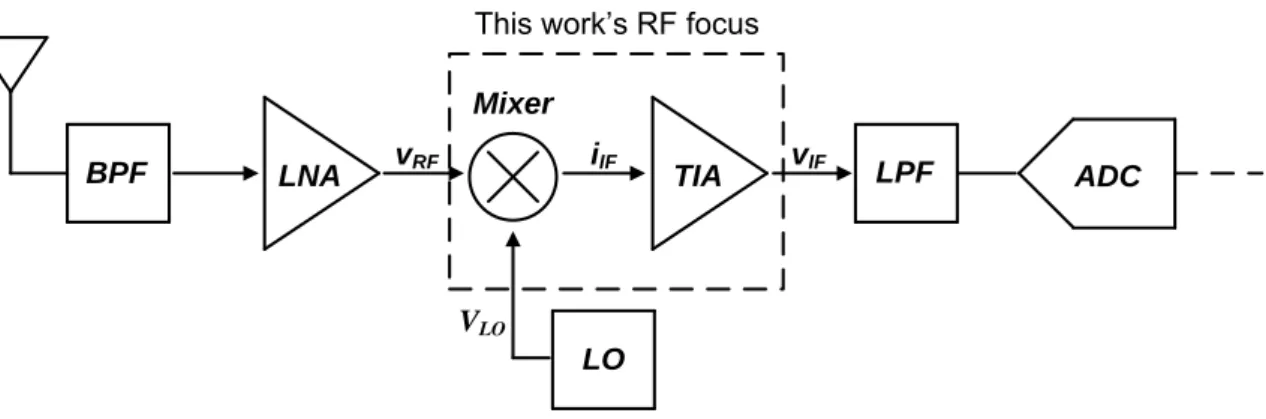
vRF iIF Mixer LNA TIA BPF LO LPF ADC vIF VLO
This work’s RF focus
Figure 2.7 – Block diagram of a heterodyne receive r architecture with focus on the mixer and TIA.
The focus, regarding the RF front-end, is to study the application of the RCG TIA topology driven by the output current of a basic hypothetical passive mixer.
Ideally, a mixer is a circuit that can be viewed as an analog multiplier circuit [29]. Such circuit has the function of translating a carrier signal from one frequency to another [30]. In a generalized manner such block can be defined as a three-port device consisting in a Local Oscillator (LO), Radio Frequency Input (RF IN) and Intermediate Frequency Output (IF OUT) as represented by Fig. 2.8.
vRF
VLO
iIF
Figure 2.8 – Block diagram of a mixer.
15
It should be noted that in Fig. 2.8 the output of the mixer, IF OUT, comes in the form of a current when there is a low load impedance at its output, thus, the need of a TIA to convert it into a suitable voltage. The LO usually consists in a large signal with fixed amplitude avoiding, this way, a small signal analysis of the active devices. By multiplying both entry signals, the mixer will produce sum and difference frequencies, along with other spurious tones, due to even and odd harmonics present within each signal. Therefore, and because multiplication in the time domain corresponds to convolution in the frequency domain, it can be easily observed that the spectral density around will be translated to [29] as Fig. 2.9 suggests.
wLO wRF
wRF - wLO w
|A|
Figure 2.9 – Example of frequency down-conversion in heterodyne receivers.
In this case, the negative components of the frequency are not of interest and have been neglected. Also neglected, the components in have no practical interest and, as such, must be
filtered using a Low-Pass Filter (LPF) function. This leaves the signal’s spectral density at
in an operation called down-conversion mixing. In heterodyne receiver architectures
the LO uses a frequency different from the RF signal resulting an IF signal with non-zero frequency.
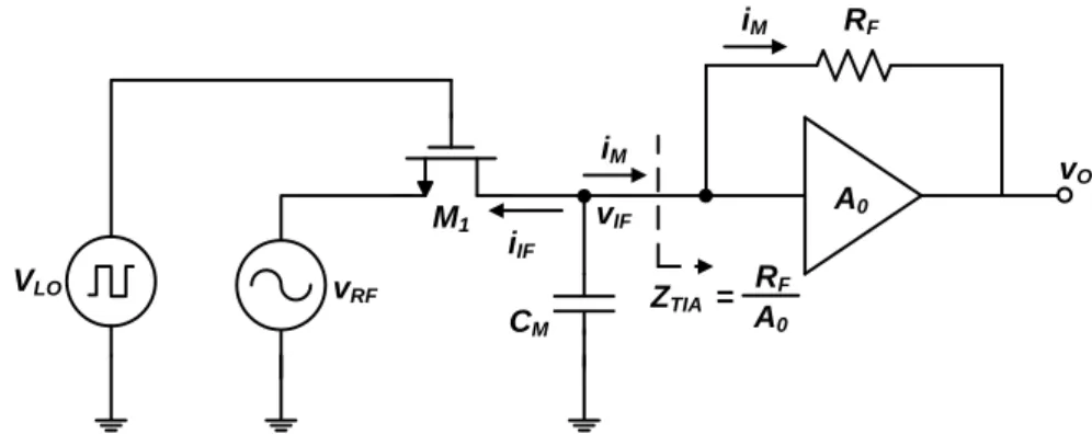
The design of a mixer can be somewhat complex and it can be distinguished between an active and a passive device, depending on providing or not providing signal amplification, respectively [29]. In the present work a basic passive mixer, which consists on a switching device controlled by the LO, is considered. Basically, the mixer considered is nothing but a MOS transistor sized to operate in the triode region. When in this region, the MOS transistor can perform as a switch if the remaining resistances present in the circuit are much higher than the equivalent resistance of the MOS device conduction channel [31], as shown by Fig. 2.10. In these conditions, the device will operate as an open switch every time 𝑉 is at low level and as a closed
switch, with an equivalent resistance, when 𝑉 is at high level. The load impedance, ,
i.e., the equivalent impedance seen at the input of the TIA, has the function of converting the mixer’s output current into an output voltage. In the design shown further on, this resistor is replaced by the TIA’s equivalent input impedance in parallel with the mixer’s output capacitance, . As in the radiation detector case, the mixer can be resumed to an equivalent current source, , in parallel with its output capacity. Regarding the design shown further ahead, it was
16
considered that the mixer had a sinusoidal output current with amplitude of 1µA with frequency around 10 MHz. Note that the mixer’s output capacity, , is mostly determined by the parasitic capacitances of the active device responsible for the switching in the mixer. This equivalent capacity was established to be around 0.1 pF, since the device does not need to be considerably large. M1 RF VLO vRF vIF iIF CM A0 iM iM vO ZTIA = RF A0
Figure 2.10 – Schematic of a basic mixer with its equivalent output capacitance and TIA’s equivalent input impedance.
Even though the basic mixer may present a simple enough design, there is a serious consideration that must be taken into account. In order to operate in the triode region, the transistor must have a very low 𝑉 voltage. This means that if the output current is too high,
correspondently low load impedance must be chosen. Otherwise, any variation in will cause
𝑉 to rise leading the transistor to other non-suitable operating regions. Regardless, can
never have high amplitude since it will make the transistor leave the triode region. This is a key restriction and it will influence the design of the TIA in an RF context since its input impedance will have to be suitable for a low variation of .
2.3.
B
ASIC
A
MPLIFICATION
T
OPOLOGIES
n this sub-chapter a detailed insight into some amplification topologies will be given. Firstly, the basic amplification stages used – the CG and Common-Source (CS) stages – will be studied. Concepts such as their voltage gain, noise analysis, incremental and dc operation modes and frequency response will be shown in order to fully understand the transimpedance topologies. Afterwards, two of the most common TIA topologies, the feedback TIA and CG TIA will be shown, their transfer functions and noise transfer functions will be derived, allowing for a deep comprehension of these topologies.
17
2.3.1. Common-Source Voltage Amplifier
he CS stage is one of the most basic amplifier configurations. Due to its relatively high voltage gain and input impedance, it is normally a configuration of choice in order to realize the input stages of Operational Amplifiers (OpAmp), even though its frequency response has a narrow band characteristic. Regardless, improvements such as source degeneration can be made to this configuration in order to increase its passing band, lowering the gain and raising the bandwidth, maintaining a constant Gain-Bandwidth Product (GBW).
In this configuration the signal is applied to the gate of the MOS device which is physically isolated from the transistor’s conduction channel. In practical terms this means that, for low frequencies, the input impedance of the transistor is high enough to be considered infinite. The CS configuration, which is represented in Fig. 2.11, can be applied with passive or active load. In the first there is a resistor connected from the power source to the drain of the transistor and, in the latter, the load impedance is accomplished by using a current source with an equivalent dynamic impedance. With active load, the configuration is able to present a higher voltage gain since it makes use of the nonlinear, large-signal transistor equations to create simultaneous conditions of large bias currents and large small-signal resistances [32].
VDD vO vI M1 ID VDD vO vI M1 RD a) b)
Figure 2.11 – Common-source configuration with: a) passive load; b) active load.
In the present chapter there will not be a clear distinction between active or passive load and, therefore, the symbol will be used to identify any of the respective resistances. In Fig. 2.12 a graphical approach to the CS large and small signal analysis is shown. The large signal or dc operating point for each value of 𝑉 , with , is the intersection between the
characteristic of with the load curve. Note that the dc operating point contemplates only
the dc component of each . Regarding the incremental output quantities, and , these can
be obtained by analyzing the incremental component of the input voltage, . Since the circuit is
approximately linear with small amplitude , results that and will be proportional to the
18
first. Once rises excessively and will present a certain amount of distortion due to the
quadratic form of the MOS transistor characteristic [31], [33].
vDS iD VDD/RD ID VDD id vds VDS t t VGS1 VGS2 VGS3 VGS4
Figure 2.12 – Graphical analysis of CS configuration (adapted from [31]).
The low frequency incremental, or small-signal, model of the CS configuration is the one shown in Fig. 2.13. The incremental input voltage, , is the controller for the output drain
current, , which is then converted to an output voltage, here represented by , by the parallel impedance constituted by the load and the equivalent conduction channel resistances.
vo
rds RD gmVgs
vi
vgs
Figure 2.13 – Low frequency incremental model of the CS configuration.
The open-loop voltage gain, , of this amplification stage can be easily deducted and, by
inspection, it follows:
(2.5)
where is the transconductance of the MOS device and is the resistance associated to the
device’s conduction channel. In the majority of cases, principally when using passive load, . This will make the conduction channel’s equivalent resistance negligible, resulting
19
(2.6)
The input impedance in this configuration tends to be infinite since the gate is isolated from the conduction channel. The output impedance, in low frequency, is also high and it can be viewed as
(2.7)
In order to evaluate and identify any noise source that can influence the behavior of the circuit, Fig. 2.14 shows the incremental model of this configuration with its noise sources. In order to obtain the effects they cause in the output of the circuit, one can identify every noise source present in the model and, assuming they are all independent from each other, evaluate the power each noise source produces [34]. Following the superposition theorem, the total output noise power will be the sum of the contributions of each noise source, assuming that the noise sources are uncorrelated.
rds RD gmVgs vgs I2n,1 I2n,Rd RS V2n,Rs V2n,out
Figure 2.14 – Incremental CS model with respective noise sources.
Since the circuits here designed operate in high frequency, the flicker ( ) noise is being neglected. The main contributions for the output noise power are the transistor’s conduction channel thermal noise current, , the load resistance equivalent thermal noise current, and
the input signal’s Thévenin equivalent thermal noise voltage source, 𝑉 . This way, each noise
source has a contribution to the total output noise power that follows:
𝑉 (2.8)
20 𝑉
𝑉 (2.10)
where is the Boltzmann’s constant, represents the absolute temperature in Kelvin and is the transistor’s noise coefficient, a parameter dependant on the size of conduction channel’s length ( if long channels are chosen and for short channel transistors). The total output noise power is nothing but the contribution of each source, i.e.
𝑉
𝑉 𝑉 𝑉 (2.11)
The high frequency model of the CS stage is slightly more complex since it includes the parasitic capacitances of the p-n junctions of the device. In Fig. 2.15 this model is shown, contemplating the three most preponderant parasitic capacitances present in the circuit.
vo rds RD gmVgs vi vgs Cgs Cgd Cdb
Figure 2.15 – High frequency model of the CS configuration.
In this configuration there are only three major capacities. In other configurations a parasitic capacity between the bulk and source of the device can be also modeled, but since this configuration has the bulk shunted with the source, which means there is no body effect, that capacity, , is short-circuited and, therefore, not present.
The high frequency gain of the CS configuration can be found by applying the Kirchhoff Current Law (KCL) in the output node, resulting
(2.12)
The gain of the configuration can then be obtained by rearranging the expression:
𝑉 𝑉 (2.13)
21 which corresponds to
𝜏
𝜏 (2.14)
where 𝜏 is related to the zero associated with capacity , 𝜏 is the time-constant associated
with the output node and is the low frequency gain.
At higher frequencies the input impedance ceases to be infinite. This is motivated by the appearance of the parasitic capacitances present at the gate of the transistor. By Miller’s theorem (see appendix A) the parasitic can be replaced by a Miller impedance, connected between
the gate and ground of the transistor with value
(2.15)
The input impedance can then be defined as the parallel between the Miller impedance and the impedance of , following
(2.16)
Developing the expression and substituting (2.5), (2.15), (2.16) and knowing that , a
simplified expression for the input impedance can be obtained [34].
(2.17)
The output impedance of this configuration can be found by inspection, as in the low frequency case, by nullifying the input voltage source. Thus it will be constituted by the parallel present at the output node, which comprises the conduction channel equivalent impedance, the load impedance and the impedances originated by the parasitic capacities and . Thus, it
will be 𝑉 (2.18)
22
2.3.2. Common-Gate Voltage Amplifier
n RF circuit design it is usually necessary to match the amplifier’s input impedance to the transmission line impedance, which is typically 50 Ω. The CG configuration can provide an easier adaptation to these impedances since its input impedance is usually much lower than in the CS stage case, making it easier to achieve the typical characteristic impedance of the transmission line. This configuration bandwidth, as will be further seen, is similar to the one of CG stage. In Fig. 2.16 the basic CG configuration is shown with passive and active load.
VDD vO VBIAS M1 ID b) vI VDD vO VBIAS M1 RD a) vI
Figure 2.16 – Common-Gate configuration with: a) passive load; b) active load.
In this configuration the gate of the MOS device is connected to a biasing dc voltage. The input signal is applied to the source of the transistor, which will present a voltage making the
body effect non-negligible. One important characteristic of this configuration, which is exploited in the present work, is the fact that the input signal can now come in the form of a current, being suitable to amplify the PSD’s output current.
When analyzing the incremental model, present in Fig. 2.17, one can find the expressions that characterize the low frequency open-loop gain, input and output impedance. Note that in this configuration there is a voltage-controlled current source, dependant on , motivated by the
body-effect. vo rds RD gmVgs vsb = vi vgs = -vi Bulk gmbVsb Source
Figure 2.17 – Low frequency incremental model of the CG configuration.
23
In this case the current source originated by the body effect is actually beneficial. If one takes into account that the current that passes through the device will be proportional
to . Therefore, the body effect actually boosts the total transconductance of the
configuration in about 10 to 30 percent, since is about 7 to 9 times lower than . Similarly
to the case of the CS stage, the low frequency open-loop gain of this configuration can be easily found with the aid of KCL, following:
(2.19)
and if ,
(2.20)
The low frequency input impedance of this amplification stage can be found by applying KCL to the input node, resulting in
(2.21)
Note that if the input impedance will simply result in
(2.22)
Regarding the noise analysis, the same procedure as the one presented in the CS stage can be made. Fig. 2.18 shows the incremental model of the CG configuration with all noise sources included, except for the low frequency flicker noise source for the reason previously stated.
rds RD gmVgs vgs g mbVsb V2n,Rs RS I2 n,1 I2 n,Rd V2 n,out
24
The main noise contributors for the output total noise power are the same as in the CS case. Therefore, by inspection, one can identify the transistor’s conduction channel thermal noise current, , the load resistance equivalent thermal noise current, and the input signal’s
Thévenin equivalent thermal noise voltage source, 𝑉 as being [34]:
𝑉 (2.23) 𝑉 (2.24) 𝑉 (2.25)
The total output noise power can then be contemplated as the sum of all noise sources, as in (2.11), providing they are all uncorrelated from each other.
At higher frequencies this configuration becomes significantly more complex than the previous. In Fig. 2.19 the high frequency incremental model of the CG configuration is presented, showing its most preponderant parasitic capacities.
vo rds RD gmVgs vsb = vi vgs = -vi Bulk gmbVsb Source Cgd Cgs Cdb Csb
Figure 2.19 – High frequency incremental model of the CG configuration.
In order to simplify the schematic, a few equivalencies can be made. Note that capacities
and are connected to the same two nodes and can be replaced by an equivalent capacity
. Likewise, the same can be made to and resulting . A
further simplification can be made if one takes into account an equivalent impedance, , that comprehends the parallel between and as Fig. 2.20 suggests [34].
25 vo rds ZL (gm+gmb)Vgs vsb = vi vgs = -vi Bulk Source CS
Figure 2.20 – Simplified model for the high freque ncy CG stage.
Thus, can be written in the following form:
(2.26)
The high frequency gain can be easily obtained if KCL is applied to both input and output nodes resulting in
𝑉 𝑉
(2.27)
Regarding the high frequency input impedance, a simplified version of it can be found.
𝑉
(2.28)
2.3.3. Common-Gate Transimpedance Amplifier
he CG TIA uses the CG configuration in order to accomplish, not only a transimpedance gain, but also current-to-voltage conversion. The output voltage of this TIA will be a function of its input current. Fig. 2.21 shows the configuration of the CG TIA in which the input current is the one provided by the PSD.
Transistor is biased by voltage 𝑉 and current . In this case, the load impedance, , can have a high enough value, presenting a parasitic capacitance, , in parallel with it. In order to find the transimpedance gain of this configuration, the small-signal model, present in Fig. 2.22, must be analyzed.
![Figure 1.1 - Representation of a PET/PEM patient interface (adaptation from [10]).](https://thumb-eu.123doks.com/thumbv2/123dok_br/15865666.1087380/20.892.186.681.453.806/figure-representation-pet-pem-patient-interface-adaptation.webp)
![Figure 2.6 – Generalized architecture of a radiation detector front -end with the TIA’s input current, , and output voltage, , shapes (adapted from [8])](https://thumb-eu.123doks.com/thumbv2/123dok_br/15865666.1087380/30.892.299.608.894.1094/figure-generalized-architecture-radiation-detector-current-voltage-adapted.webp)