PoS(TWEPP-17)044
for the BESIII CGEM Detector
Fabio Cossio∗,b,eMaxim Alexeev,b, f, Ricardo Bugalho,d Junying Chai,a,b,eWeishuai Cheng,a,b,e Manuel D. Da Rocha Rolo,bAgostino Di Francesco,cMichela Greco,b, f Chongyang Leng,a,b,eHuaishen Li,a,b Marco Maggiora,b, f Simonetta Marcello,b, f Marco Mignone,b Angelo Rivetti,b Joao Varelac,d and Richard Wheadonb
aInstitute of High Energy Physics, Chinese Academy of Sciences, 19B YuquanLu, Beijing, 100049, China
bINFN, Sezione di Torino,
Via P. Giuria 1, 10125 Torino, Italy
cLaboratório de Instrumentação e Física Experimental de Partículas (LIP), Av Elias Garcia 14, 1000-149, Lisbon, Portugal
dPETsys Electronics,
Taguspark Edificio Tecnologia 1, Oeiras, Portugal
ePolitecnico di Torino, Dipartimento di Elettronica e Telecomunicazioni, Corso Duca degli Abruzzi 24, 10129 Torino, Italy
f Universitá di Torino, Dipartimento di Fisica, Via P. Giuria 1, 10125 Torino, Italy
E-mail:[email protected]
TIGER (Turin Integrated Gem Electronics for Readout) is a mixed-mode ASIC for the readout of signals from CGEM (Cylindrical Gas Electron Multiplier) detector in the upgraded inner tracker of the BESIII experiment, carried out at BEPCII in Beijing. The ASIC includes 64 channels, each of which features a dual-branch architecture optimized for timing and energy measurement. The input signal time-of-arrival and charge measurement is provided by low-power TDCs, based on analogue interpolation techniques, and Wilkinson ADCs, with a fully-digital output. The silicon results of TIGER first prototype are presented showing its full functionality.
Topical Workshop on Electronics for Particle Physics 11 - 14 September 2017
Santa Cruz, California
PoS(TWEPP-17)044
1. Introduction
The BESIII (Beijing Spectrometer III) Experiment operates since 2009 at the Beijing
e+e-collider (BEPCII), hosted by the Institute of High Energy Physics (IHEP) [1]. The inner drift
chamber is suffering early aging due to the increased machine luminosity, which has reached 1.0 x 1033 cm−2s−1. To overcome this aging effect an upgrade based on CGEM (Cylindrical Gas Electron Multiplier) technology has been proposed. The installation of the new detector is scheduled to take place during the 2018 upgrade and the project features three independent track-ing layers, each made of a cylindrical triple-GEM detector, which allows for high gains and low discharge probability [2]. The analogue readout of the CGEM employs charge centroid and micro-TPC algorithms to improve the spatial resolution to better than 130 µm while increasing the strip pitch to 650 µm, thus reducing the total number of channels to about 10 000 [3]. These channels are readout by a dedicated front-end ASIC, TIGER (Turin Integrated Gem Electronics for Readout), which has been designed to address the needs of the CGEM tracker.
2. TIGER ASIC architecture
TIGER is a mixed-signal 64-channel ASIC developed to readout the CGEM detector of the BESIII Experiment. It has been designed in a 110 nm CMOS technology to operate with a 1.2 V power supply and occupies an area of 5 mm x 5 mm. Table1reports the most important specifica-tions of the ASIC.
Parameters values Input Capacitance Up to 100 pF Data Rate 60 kHz/ch Input Charge 3-50 fC Time resolution 5 ns ENC < 2000 e− Power Consumption < 12 mW/ch
Table 1: Design specifications of the TIGER chip.
The architecture of one channel is shown in Fig.1and includes signal amplification, shaping
and processing. The analogue front-end consists of a charge sensitive amplifier and a dual-branch shaper with different peaking times, optimized for timing (Time Branch) and charge (Energy Branch) measurement. Two separate discriminators with independent programmable thresholds generate the trigger signals for the channel controller, a digital logic block working at 160MHz clock frequency, that manages the channel operations. The timing information is provided by low-power quad-buffered TDCs based on analogue interpolation, producing a sub-50 ps time mea-surement (Tfine) [4]. The charge measurement can be extracted either exploiting the Time-over-Threshold (ToT) technique or with a sample-and-hold circuit (S/H), connected at the output of the slow shaper and acting as a digitally controlled peak detector. A Wilkinson ADC, which is shared with the TDC operation, digitizes the sampled signal into a 10-bit word (Efine).
In addition, a test pulse (TP) signal can be sent either to the front-end, allowing to test the whole readout chain or directly to the channel controller for the TDCs calibration. The front-end
PoS(TWEPP-17)044
Figure 1: Block diagram of one channel (left) and one output event word (right).TP is generated by an internal calibration circuit and its user-configurable amplitude enables to explore the full input dynamic range. The digital logic and the output interfaces of the ASIC have been inherited from the TOFPET2, an ASIC developed for medical applications. More details can
be found in [5,6]. Due to the radiation environment of the BESIII Experiment, it has been protected
against Single Event Upset (SEU) by using Hamming encoding and Triple Modular Redundancy (TMR).
3. Test setup
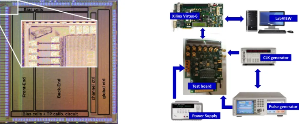
The tests of the first TIGER prototype, produced in a Multi-Project-Wafer (MPW) run, started in November 2016. Fig. 2 shows the test bench setup used to characterize the ASIC: the setup includes an FPGA board, power supplies, a low-jitter reference clock source and a pulse generator. The ASIC test board, designed and assembled by the Turin INFN electronics group, comprises five trimmers for the ASIC biasing, 2 SMA LVDS inputs to feed the clock to the chip and 8 SMA LVDS debug outputs. The test board also provides direct outputs from the shaper and threshold of the channel 63 timing branch which can be probed to bypass the digital back-end and assess only the analogue very front-end of the chip. An Agilent E3631A 80W Triple Output Power Supply module provides separated DC power supplies for the analog and the digital domains.
Bias cells + TP calib.circuit Bias cells Fr on t-E nd B ac k-En d ch an ne l c tr l gl ob al c tr l
Xilinx Virtex-6 LabVIEW
Power Supply
CLK generator
Pulse generator Test board
Figure 2: Microphotograph of the TIGER chip (left) and the test bench setup used for the electrical charac-terization (right).
PoS(TWEPP-17)044
The ASIC test board is connected to the FPGA board, a Xilinx Virtex 6 Evaluation board (ML605 Evaluation kit), that manages the ASIC configuration, data transmission and TP genera-tion. A PC runs the data acquisition through a LabVIEW interface with online monitoring. The 160 MHz clock can be synthesized either by the FPGA board or with a low-jitter Stanford Research CG635 Clock Generator (1 µHz to 2.05 GHz square wave generator). An Agilent 81133A Single Channel 3.35 GHz Pulse Pattern Generator has been used to inject a known charge at the debug port installed on channel 63 input in order to calibrate the internal test pulse.
4. Results
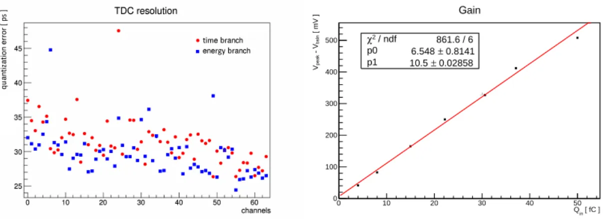
First, the TDC performance has been evaluated by feeding a digital TP at the inputs of the TDCs and scanning its phase along one clock cycle. These measurements allow to create an offline look-up table (LUT), in which the stored values are used for the offset and gain correction of each
TDC. The left plot of Fig.3shows the TDC time resolution for the time and energy branch of the 64
channels after the calibration. The quantization error is less than 50 ps r.m.s., with good uniformity across the chip. This value is much lower than the required time resolution, therefore the timing performance of the channel will be only affected by the response of the analogue front-end. This methodology allowed also to prove the correct behaviour of the back-end electronics.
The front-end gain and the S/H circuit performance have been evaluated using the external pulse generator to inject a known input charge at the input of channel 63, scanning the full dynamic range. The right plot of Fig.3shows the pulse amplitude measured at the output of the fast shaper for different values of input charge. The resulting gain of 10.5 mV/fC is in good agreement with the 10.75 mV/fC expected gain from post-layout simulation.
45 40 • 30 25 o TDC resolution • • • • • • • •• • • • • • • • • •• • • • • • •• • •• • ••• • • • • ••• ••• •• •••• • • • • • • •• • • • • 10 20 30 • • ••• • • • • •• • •• • • ••• • • •• • • •• 40 • • •• • •••• • • • • •••• 50 • • • • •• •••• • •• •••• • 60 channels qu an tiz atio n e rror [ ps ] time branch energy branch • • [ fC ] in Q 0 10 20 30 40 50 Vpeak - V bsln [ mV ] 0 100 200 300 400 500 χ2 / ndf 861.6 / 6 p0 6.548 ± 0.8141 p1 10.5 ± 0.02858 / ndf 2 χ 861.6 / 6 p0 6.548 ± 0.8141 p1 10.5 ± 0.02858 Gain
Figure 3: TDC resolution (left) and front-end gain (right).
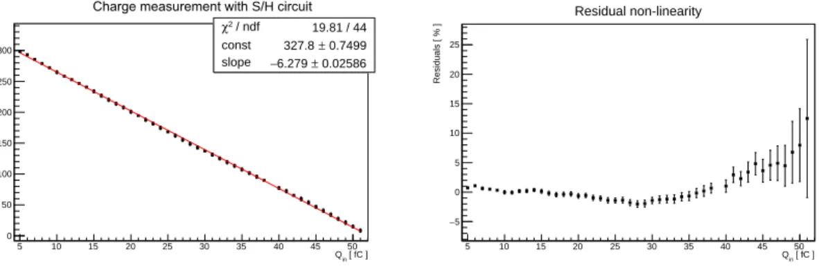
Fig.4shows the results of the charge measurement using the S/H circuit. The linearity is very good (less than 2%) up to 40 fC, with a degradation for higher input signals mainly due to the saturation of the analogue front-end. On the other hand, the ToT technique, due to the intrinsic non-linear pulse duration of CR-RCnshapers, would require a ToT vs. Qin calibration, but given
the good performance of the S/H circuit it is not planned to operate in the experiment the ASIC in ToT mode.
PoS(TWEPP-17)044
[ fC ] in Q 5 10 15 20 25 30 35 40 45 50 Efine [digits] 0 50 100 150 200 250 300 / ndf 2 χ 19.81 / 44 const 327.8 ± 0.7499 slope −6.279 ± 0.02586 / ndf 2 χ 19.81 / 44 const 327.8 ± 0.7499 slope −6.279 ± 0.02586Charge measurement with S/H circuit
[ fC ] in Q 5 10 15 20 25 30 35 40 45 50 Residuals [ % ] 5 − 0 5 10 15 20 25 Residual non-linearity
Figure 4: Charge measurement with S/H circuit: dynamic range (left) and residual non-linearity (right).
5. Outlook and Conclusions
A dedicated 64-channel ASIC, called TIGER, has been designed for the analogue readout of the BESIII CGEM tracker. The results from the electrical characterization of the first prototype show the good performance of the ASIC. All the detector requirements are met within the limited power budget of 12 mW per channel, tests with the sensor using cosmic rays and radioactive sources are now ongoing. A new version, featuring minor design revisions, has been submitted for mass production in August 2017, in order to be tested and qualified for the detector installation which is scheduled for Summer 2018.
Acknowledgments
This research activity has been performed within the BESIIICGEM Project, funded by Euro-pean Commission in the call H2020-MSCA-RISE-2014.
References
[1] BESIII Collaboration, The construction of the BESIII experiment, Nucl. Instr. Meth. A, 598 (2009) pg. 7-11, https://doi.org/10.1016/j.nima.2008.08.072
[2] BESIII Collaboration, BESIII Cylindrical GEM Inner Tracker. Technical report, July 2014.
[3] L. Lavezzi et al., The Cylindrical GEM Inner Tracker of the BESIII experiment: prototype test beam results, Journal of Instrumentation, 12 (2017) C07038
[4] A. Rivetti et al., A pixel front-end ASIC in 0.13 µm CMOS for the NA62 experiment with on pixel 100 ps Time-to-Digital Converter, Proceedings of IEEE NSS-MIC 2009, doi:
https://doi.org/10.1109/NSSMIC.2009.5401882
[5] M.D. Rolo et al., TOFPET ASIC for PET applications, Journal of Instrumentation 8 (2013) C02050
[6] A. Di Francesco et al., TOFPET2: a high-performance ASIC for time and amplitude measurements of SiPM signals in time-of-flight applications, Journal of Instrumentation 11 (2016) C03042