Brazilian Journal of Physics, vol. 29, no. 4, December, 1999 797
Observation of Low Frequency Oscillations in
GaAs Samples Grown by Molecular Beam
Epitaxy at Low Temperatures
R.M. Rubinger,A. G. deOliveira,G. M. Rib eiro,D. A. W. Soares
,
and M.V. B.Moreira
Departamento de Fisica, Universidade Federal de Minas Gerais CP 702, 30123-970 Belo Horizonte, Brazil
Received February, 1999
We have observed Low Frequency Oscillations (LFO) in a GaAs sample grown by molecular beam epitaxy (MBE) at 300o
C as a function of applied electric eld, temperature and illumination
in-tensity. Time series of the oscillations for dierent values of the applied electric eld at room temperature were obtained. We have also obtained thejxEcharacteristics as a function of
temper-ature and light intensity. We were able to control the LFO using three experimental parameters, the electrical eld, which controls the oscillation frequency, and the temperature and illumination intensity, which control the carrier density and eld-enhanced trapping. We were able to identify the LFO dependence on the carrier density and on the eld-enhanced trapping.
I Introduction
Low frequency oscillations (LFO) are detected in the external current of semiconductor devices in the range of sub-Hz to few hundreds Hz. Inside the device they constitute self-organized spatio-temporal structures of the type of electric eld domains moving from the cath-ode to the ancath-ode. Because of their low frequency, os-cillations are easy to be observed and analyzed since no sophisticated instrumentation is needed in order to carry out measurements. It is also worth to mention that semiconductors are one of the most easily repro-ducible systems for the study of nonlinear dynamics and deterministic chaotic phenomena. In this way, LFO in semi-insulating (SI) material are a good theme for such studies.
We have studied thejxEcharacteristics of a GaAs
sample grown by MBE at 300o
C looking for LFO and
routes to chaos of the LFO [1,2,3]. In semiconductors presenting negative dierential conductivity (NDC), moving high-eld domains can build up spontaneously leading to current oscillations. Such oscillations occur due to the eect of eld enhanced trapping of carriers been captured into deep traps. The low temperature MBE growth (LT-MBE) of GaAs leads to a high den-sity of intrinsic defects, mainly in the form of antisite defects, namely As atoms in the Ga site (AsGa). These
defects are ecient in inducing eld enhanced trapping. For this work typical samples were cut in small rectan-gles and two indium contacts were dened separated in about 200m. Samples grown at low temperatures
are photo-sensitive, and therefore, measurements under illumination using an infrared LED were carried out. The frequency of the oscillations is a strong function of temperature and illumination intensity. We have ob-served the presence of LFO in the range of sub-Hz to few Hz for external electrical elds ranging from Vcm,1 to
kVcm,1. The denition of the intrinsic defect directly
involved with LFO has been historically a hard job but our experimental setup and the sample provided favor-ably simple conditions to study it, since we have three control parameters, namely, the applied voltage, the temperature and the light intensity. These experimen-tal parameters are easy to control with high accuracy and, in this way, we expect to be able to tune route to chaos.
The analysis of the temperature dependence of LFO has been used by other authors in order to identify deep levels in SI crystals [4]. Particularly, the Arrhe-nius plots of the frequency modes of the LFO have been used to obtain information for GaAs [5] and InP [4] and the authors claim that this procedure has many advan-tages over others. A model that describes completely the phenomenology is not yet available but some
798 R.M.Rubingeret al.
proaches have been proposed based on the eects of eld-enhanced trapping [5], eld-enhanced emission [3] and negative dierential mobility [6].
In this paper we study the LFO in a LT-MBE GaAs sample. These samples presents high density of deep level defects, which gives them semi-insulating (SI) characteristic since the Fermi level is pinned around the middle of the gap. Under illumination intrinsic defects release carriers into the conduction and valence bands. At room temperature, we have measured the depen-dence of the LFO and its characteristic frequencies as a function of the electric eld. The temperature and the illumination dependence of ourjxEcharacteristics
give evidences of eld enhanced trapping of free carriers in both the valence and conduction bands is the most probably model.
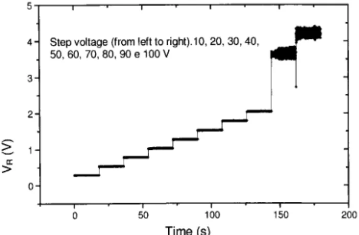
Figure 1. LFO as a function of time and applied bias. Each step corresponds to a bias, which is 10V in the left and in-creases 10V for each step to the right. The Y axis is the voltage through a 1M series resistor.
II Results
The electric eld dependence of the LFO observed at room temperature is shown in Fig.1. We can see that the amplitude of the oscillations increases with the value of the applied electric eld. For measurements carried out with an electric eld of 1500 Vcm,1 (90V)
and 1670 Vcm,1 (100V) the increase in the amplitude
of the LFO signal is more remarkable. This is explained based on the observed fact that the sample has an enor-mous enhancement in the free carrier density due to impurity breakdown in shallow acceptors. In Figs. 2 and 3 we show the LFO obtained at 330 Vcm,1(20V)
and 1500 Vcm,1 (90V). The signal obtained at 330
Vcm,1is clearly a combination of two frequencies with
the main frequency centered in 2.35Hz. At 1500 Vcm,1
we can observe an increase in the amplitude and fre-quency, which is about 4.3Hz.
Figure 2. A zoom of Fig. 1 for the step of 20V. Observe that the main frequency is of 2.35Hz.
Figure 3. A zoom of Fig.1 for the step of 90V. Observe that the main frequency is of 4.3Hz.
For measurements carried out at 2000 Vcm,1
(120V) we calculated the Fourier transform and the presence of many peaks were obtained. The main peak locates at frequency zero, i.e. a constant term and the other peaks are listed in the table.
Fr eq uency(Hz) Rel ativ eIntensity
0 1
2:8 0:0044
4:7 0:0049
5:6 0:066
10:8 0:011
11:3 0:017
If we neglect the two peaks at 10.8 and 11.3Hz, that at 2.8Hz is the half of the frequency of the 5.6Hz peaks. This fact is compatible with a bifurcation of cycle two. In Fig. 4 we show thejxEcharacteristic as a
Brazilian Journal of Physics, vol. 29, no. 4, December, 1999 799 trapping in a deep level trap. Besides, NDC is
observ-able for measurements using 30mA trough the LED. Amplitude oscillations are easily observed in the sub-linear regime and they increase with the electric eld.
Figure 4. jEcharacteristic at 130K as a function of the
illumination intensity. The three like form of the curves is a kind of Poincare map of the LFO route to chaos.
In Fig. 5 we can observe a situation where the ef-fect of eld enhanced trapping is still stronger than those presented in Fig. 4. In this case, the NDC re-gion presents LFO but with amplitudes much smaller than those observed at 130K. Fig. 6 shows at 20K an increasing eciency in the eld enhanced trapping and very complex LFO windows. Here the maximum of the current density for the highest illumination intensity is 5 times higher than the values observed at 100K.
Figure 5. jE characteristic at 100K as a function of
the illumination intensity. At this temperature the eld en-hanced trapping eect is more eective, showing a N type NDC region for the three highest illumination intensity.
Figure 6.jEcharacteristic at 20K as a function of the
il-lumination intensity. At this temperatre the highest current is 5 times the highest current at 100K and eld enhanced trapping with LFO windows are presented.
III Discussion
For the results shown in Fig. 1 we deduce that, at room temperature and in darkness, the oscillation fre-quency is a function of the applied eld. The ampli-tude also seems to increase with the eld but only af-ter a threshold of impurity breakdown. Afaf-ter a critical electric eld, which is between 1500 and 2000Vcm,1,
the LFO starts to present bifurcations of the main fre-quency. At room temperature we cannot obtain similar
jxEcharacteristics to those found in the literature for
the SI GaAs grown by liquid encapsulated Czochral-ski (LEC) [7]. ThejxEcharacteristics are determined
mainly by the impurity breakdown eect at this tem-perature. We know that the optical cross section and carrier life-time of deep trap present in our sample favor an increasing electron density for decreasing tempera-ture and increasing light intensity. At 130K however we reach the conditions that we have succeeded in obtain-ing similar data published in Ref. 7. Since our sample has a deep trap density of about three orders of magni-tude higher than LEC samples we believe that the free carrier density rather than the impurity density is the important parameter in order to dene improvements in the LFO characteristics.
For temperatures lower than 130K eld-enhanced trapping increases its dependence on the electrical eld and a N shaped NDC region is observed. At this situa-tion the intensity of the LFO are less strong when com-pared to the zero frequency term. Below 20K we can see LFO windows in thejxEcharacteristics. We believe
800 R.M.Rubingeret al.
the free carrier density in the , valley of the conduction band. For a free carrier density high enough to form dipole domains of the Gunn type the eld enhanced trapping could induce the recombination of the free electrons of the , valley with ionized deep donors re-sulting in monopole domains which moves slower since the eective mass at the upper valleys of the conduction band is higher. Electrons in the L or X valleys recom-bine less eciently with the deep level defects due to its dierences in the K space. A low carrier density or a highly ecient eld enhanced trapping eect (high temperature and below 130K respectively) results in the destruction of the LFO monopoles before they reach the anode.
In summary, we have measured LFO in an LT-MBE GaAs sample grown at 300o
Cas a function of the
electrical eld, temperature and illumination intensity. With these three parameters we were able to control the LFO characteristics. The electrical eld controls the oscillation frequency, the temperature and illumination
control the carrier density and the eld-enhanced trap-ping characteristic. We were able to identify how the LFO of our sample depends on the carrier density and on the power of eld-enhanced trapping.
References
[1] G.N. Maracas and D.A. Johnson, Appl. Phys. Lett.46,
305 (1985).
[2] E. Scholl, Phys. Rev. B34, 1395 (1986).
[3] E. Scholl, Phys. Scrip. T29, 152 (1989).
[4] C. Backhouse, L. Young: Solid State Electr. 35, 1601
(1992).
[5] H.K. Sacks, A.G. Milnes: Int. J. Elect.28, 565 (1970).
[6] S.P. McAlister, Z.-M. Li, D.J. Day: Canadian J. Phys.
69, 207 (1991).