Outubro, 2015
Nuno Miguel Teixeira Coelho
Licenciado em Ciências de Engenharia de Micro e Nanotecnologias
Improving Silicon Probe Performance Through
Layer-by-Layer Coating
Dissertação para obtenção do Grau de Mestre em
Engenharia de Micro e Nanotecnologias
Orientador: Adam Kampff, Professor Doutor,
Champalimaud Center for the Unknown
Co-orientadores: Elvira Fortunato, Professora Doutora,
Faculdade de Ciências e Tecnologia da Universidade Nova de Lisboa
Improving Silicon Probe Performance Through Layer-by-Layer Coating
ii
Improving Silicon Probe Performance Through
Layer-by-Layer Coating
Copyright © Nuno Miguel Teixeira Coelho
Faculdade de Ciências e Tecnologia da Universidade Nova de Lisboa
A Faculdade de Ciências e Tecnologia e a Universidade Nova de Lisboa têm o direito,
perpétuo e sem limites geográficos, de arquivar e publicar esta dissertação através de
exemplares impressos reproduzidos em papel ou de forma digital, ou por qualquer outro
meio conhecido ou que venha a ser inventado, e de a divulgar através de repositórios
científicos e de admitir a sua cópia e distribuição com objectivos educacionais ou de
Improving Silicon Probe Performance Through Layer-by-Layer Coating
iv
“Time you enjoy wasting, was n
ot
Improving Silicon Probe Performance Through Layer-by-Layer Coating
vi
Acknowledgements
What a harsh and also fun dissertation this was. For starters, I would like to thank eve-ryone that made this huge step in my academic life possible. This project was achievable throughout 5 years of university in which fun, friendship, love, and work took part of, and it was all the people that I met and lived with that made those years so great. It’s impossible to thank each person individually that helped me through these challenging and adventurous times, and I truly hope that no one will take it personally for not making it in to this (finite) text. That said, I would like to sincerely thank the following:
To Dr. Adam Kampff for the opportunity to work with a great group in the amazing institution that the Champalimaud Centre for the Unknown (CCU) is. It was an experiment that I will remember my whole life, and where I’ve grown academically and as a person as well. All the notes, comments and remarks given were extremely useful and enlightening, and allowed me to make a master thesis that I can be proud of.
To Dr. Elvira Fortunato, for all she was done for nanotechnology around the world and especially in our university, enabling the formation of hundreds of well prepared future engi-neers.
To Joana Neto for all she had to put up with me. Since my day one till the last day, she was there to guide and help me, and I can’t thank her enough for the infinite patience. Without her, this project simply wouldn’t be possible, and I think that that says it all.
To the rest of the group that constitutes the Intelligent Systems Lab at the CCU, for turning this experience in a fun and educational time: George Dimitriadis, Pedro Lacerda, João Frazão, Joana Nogueira and Gonçalo Lopes.
To Pedro Baião, who had no obligation whatsoever to help me, and yet he did. Much of my work was supported by his previous project, and without it, this master thesis would be far less interesting.
To Tiago Monteiro for all the help with the post-surgery recordings and explanations of how the all process works. Also a very special thanks to William, the mouse that took this thesis to a all new level.
To everyone at CENIMAT/I3N that helped me and contributed to the relaxed and amaz-ing environment present there.
Improving Silicon Probe Performance Through Layer-by-Layer Coating
vii
To all the good friends that accompanied me in the best years of my life (so far, hope-fully!). To my friendship friends: Ana Castanho, André Castro, Francisco Nunes, Joana Cabral, Joana Nave, Maria João, Pedro Castanho, Pedro Palma and Rui Carreiras, for all the fun and stupid moments in school and in the innumerous coffees and night outs we had. To all my aca-demic godchildren and grandchildren that made me proud over the years. To Constança Oliveira, Joana Almeida e Sofia Martins for all the patience and love, and for helping me be the men I am today (for better or worse!). Finally, last but not least, to my best friends over the years: Afonso Ferreira, Daniel Pereira, Diogo Vaz, João Jacinto, João Rosa, Júlio Costa, Moisés Tereso, Pedro Figueiredo and Tiago Rosado. All of us, one way or the other were part of the great and mythic place that Basolho became, and I wanted to thank you for all the parties and unforgettable moments that we shared over the years.Improving Silicon Probe Performance Through Layer-by-Layer Coating
viii
Abstract
Fully comprehending brain function, as the scale of neural networks, will only be possi-ble with the development of tools by micro and nanofabrication. Regarding specifically silicon microelectrodes arrays, a significant improvement in long-term performance of these implants is essential. This project aims to create a silicon microelectrode coating that provides high-quality electrical recordings, while limiting the inflammatory response of chronic implants.
To this purpose, a combined chitosan and gold nanoparticles coating was produced allied with electrodes modification by electrodeposition with PEDOT/PSS in order to reduce the im-pedance at 1kHz. Using a dip-coating mechanism, the silicon probe was coated and then charac-terized both morphologically and electrochemically, with focus on the stability of post-surgery performance in anesthetized rodents. Since not only the inflammatory response analysis is vital, the electrodes recording degradation over time was also studied.
The produced film presented a thickness of approximately 50 µm that led to an increase of impedance of less than 20 kΩ in average. On a 3 week chronic implant, the impedance in-crease on the coated probe was of 641 kΩ, compared with 2.4 MΩ obtained for the uncoated probe. The inflammatory response was also significantly reduced due to the biocompatible film as proved by histological tests.
Improving Silicon Probe Performance Through Layer-by-Layer Coating
x
Resumo
De modo a compreender totalmente o funcionamento do cérebro, especialmente no que à comunicação entre os neurónios diz respeito, o desenvolvimento da micro e nanofabricação é essencial. Analisando especificamente matrizes de microeléctrodos de silício, verifica-se que o seu desempenho em implantes de longo período é ainda deficitário. Este projecto tem como objectivo a criação de um revestimento biocompatível para essas mesmas matrizes de modo a proporcionar a obtenção de sinais eléctricos sem diminuição da sua qualidade, bem como mini-mizar ao máximo a resposta inflamatória por parte do organismo.
Para este efeito, um revestimento combinado de quitosano e nanopartículas de ouro foi criado, aliado à modificação prévia dos microeléctrodos através da electrodeposição de PEDOT/PSS, de modo a reduzir a sua impedância a 1 kHz. Recorrendo a um mecanismo de imersão por camadas, o filme foi depositado sobre a sonda de silício sendo depois caracterizada morfológica e electroquimicamente, com especial foco no desempenho em implantes crónicos. Tanto o nível de resposta inflamatória como a degradação do sinal eléctrico obtido ao longo do tempo por parte dos microeléctrodos foram estudados.
O filme produzido, com cerca 50 nm leva a um aumento na magnitude da impedância de menos de 20 kΩ e posteriormente permite que um implante após 3 semanas apresente um aumento de cerca de 641 kΩ, ao invés de 2.4 MΩ num implante sem a presença do filme bio-compatível de quitosano e nanopartículas de ouro. A presença do filme originou também uma redução da resposta inflamatória por parte do organismo.
Improving Silicon Probe Performance Through Layer-by-Layer Coating
xii
Abbreviations
AFM Atomic Force Microscope
Ag Silver
AgCl Silver Chloride
Au Gold
AuNp’s Gold Nanoparticles
Chi Chitosan
DLS Dynamic Light Scattering
EEG Elecroencephalography
F-MRI Functional Magnetic Resonance Imaging
LFP Local Field Potential
O Oxygen
PBS Phosphate-buffered Saline
PEDOT Poly(3,4-ethylenedioxythiophene)
PET Positron Emission Tomography
PPy Poly(pyrrole)
PSS Poly(styrenesulfonate)
SEM Scanning Electron Microscope
Improving Silicon Probe Performance Through Layer-by-Layer Coating
xiv
Table of contents
ABSTRACT ... VIII
RESUMO ... X
ABBREVIATIONS... XII
FIGURE INDEX ... XVI
TABLE INDEX ... XVIII
INTRODUCTION ... 1
MATERIALS AND METHODS ... 6
2.1 SOLUTION-BASED SYNTHESIS ... 6
2.1.1 Chitosan ... 6
2.1.2 Gold nanoparticles (AuNp’s) ... 6
2.1.3 Poly(3,4-ethylenedioxythiophene) – Poly(styrenesulfonate) (PEDOT:PSS) 6 2.2 AUNP’S CHARACTERIZATION ... 6
2.2.1 Dynamic Light Scattering (DLS) ... 6
2.3 COATINGS CHARACTERIZATION ... 7
2.3.1 Atomic Force Microscope (AFM) ... 7
2.3.2 Scanning Electron Microscopy (SEM) ... 7
2.3.3 Contact Angle ... 7
2.4 SILICON PROBES ... 7
2.4.1 Dip-coating ... 7
2.4.2 Impedance characterization ... 8
2.4.3 Morphological Characterization ... 9
2.4.4 Electrodeposition Set-up ... 9
2.5 CHRONIC SURGERY ... 9
2.6 IN VIVO RECORDINGS ... 9
2.7 HISTOLOGICAL CHARACTERIZATION ... 10
RESULTS ... 12
3.1 COATING CHARACTERIZATION ... 12
3.1.1 Pre-Surgery Impedance Characterization ... 12
3.1.2 Morphologic Characterization ... 13
3.1.3 Contact Angle ... 15
3.1.4 Degradation Characterization ... 16
3.1.5 Endurance Test ... 16
3.2 IN VIVO RECORDINGS ... 17
3.2.1. Electrodes Impedances ... 17
Improving Silicon Probe Performance Through Layer-by-Layer Coating
xv
3.2.3. Biocompatibility Characterization ...22CONCLUSIONS AND FUTURE PERSPECTIVES ... 24
Improving Silicon Probe Performance Through Layer-by-Layer Coating
xvi
Figure Index
FIGURE 1-VARIOUS SYSTEMS CONFIGURATIONS FOR NEURAL STUDY.SINGLE TUNGSTEN WIRE WITHOUT MODIFICATIONS (A)[8];MICHIGAN PROBE, A SILICON BASED NEURAL PROBE WITH 1024 ELECTRODES
(B);FLEXIBLE PROBE ARRAY CONSTITUTED BY POLYIMIDE (C)[9]; SINGLE OPTRODE, WITH BOTH RECORDING AND STIMULATION FUNCTION. LIGHT IS THEN DELIVERED THROUGH THE FIBER,
REACHING THE NEARBY NEURONS (D)[7]. ... 2 FIGURE 2–SPIKES DETECTED FOR 10 DIFFERENT NEURONS (LEFT) AND THE LOCATION WHERE THEY WERE
MEASURED (RIGHT). DIFFERENT ELECTRODES CAN MEASURE THE SAME SIGNAL, WHERE THE ELECTRODE WITH THE HIGHEST PEAK-TO-PEAK AMPLITUDE IS CHOSEN TO BE ANALYZED.[14] ... 3 FIGURE 3–INVASIVE PROBE DIMENSIONS COMPARED WITH A HUMAN BRAIN (USUALLY THE FINAL DEPTH
OF THE IMPLANT IS ONLY OF A FEW MILLIMETERS).DESPITE THE PROBE’S SIZE IS SIGNIFICANTLY MINUTE COMPARED TO OUR BRAIN, THE SCAR FORMATION IS AN ISSUE THAT NEEDS TO BE TENDED FOR LONG TERM IMPLANTS. ... 3 FIGURE 4 – REPRESENTATION OF THE STRUCTURAL MODIFICATIONS ON SILICON MICROELECTRODE
ARRAYS.THE PROCESS BEGINS WITH THE ELECTRODES MODIFICATION WITH PEDOT/PSS, FOLLOWED BY LAYER-BY-LAYER COATING WITH CHITOSAN AND GOLD NANOPARTICLES. ... 4 FIGURE 5 – DIP-COATING PROCEDURE. SCHEMATICS OF THE DIFFERENT STEPS THAT CONSTITUTE THE
PROCESS:1,4– CHITOSAN AND GOLD NANOPARTICLES SOLUTION; 2,5– DISTILLED WATER; 3,6–
NITROGEN DRYING (A);DIP-COATING MECHANISM REPRESENTATION (B). ... 8 FIGURE 6-SCHEMATICS OF THE NANOZ TWO ELECTRODE CELL SYSTEM CONFIGURATION.THE AG/AGCL
WIRE IS USED AS REFERENCE AND IT IS LOCATED AROUND THE CUP WHILE IN CONTACT WITH THE
SOLUTION, WHEREAS THE PROBE IS POSITIONED IN THE MIDDLE OF THE DEPOSITION CUP, AT AN EQUAL DISTANCE OF THE WIRE. ... 8 FIGURE 7– IMPEDANCE VARIATION AFTER THE DEPOSITION OF THE FILM FOR BOTH PROBES.THE PROBE
COATED WITH ELEVEN LAYERS TOTAL EXPERIENCED A HIGHER AVERAGE IMPEDANCE INCREASE. ... 12 FIGURE 8-COMPARISON BETWEEN THE TWO CHITOSAN/GOLD NANOPARTICLES FILMS OBSERVED IN SEM (HIGHLIGHTED IN RED): TOTAL OF 5 LAYERS –40 NM (A); TOTAL OF 11 LAYERS –200 NM (B). ... 13 FIGURE 9 – SILICON PROBE WITH CHITOSAN/AUNP COATING OBSERVED IN SEM SHOWING SOME DUST
PARTICLES (A) AND ALSO SOME GOLD NANOPARTICLES AGGLOMERATES (B). ... 14 FIGURE 10-COATING MORPHOLOGY STUDY VIA AFM.BOTH FILMS HAVE THE SAME NUMBER OF LAYERS
DEPOSITED, ALTHOUGH IN B) THE GOLD NANOPARTICLES SOLUTION USED HAD A HIGHER CONCENTRATION COMPARED TO THE ONE IN A). ... 15 FIGURE 11–MEASUREMENT OF CONTACT ANGLE OF A PBS DROP IN CONTACT WITH CHI/AUNP COATING. ... 15 FIGURE 12-DEGRADATION OF THE CHITOSAN/GOLD NANOPARTICLES COATING ON A 37 ºCPBS SOLUTION
OVER TIME. FIRST, THE CONTROL SILICON WAFER A); COATING AFTER TWO WEEKS B); COATING AFTER FOUR WEEKS C). ... 16 FIGURE 13–VARIATION OF THE AVERAGE IMPEDANCE MAGNITUDE FOR 28 ELECTRODES (AT 1 KHZ) AFTER
COATING DEPOSITION (RED) AND AFTER ENDURANCE TEST WITH AGAR (GREEN). ... 17 FIGURE 14- VARIATION OF THE AVERAGE IMPEDANCE MAGNITUDE (AT 1KHZ) FOR THE TWO CHRONIC
SURGERY SELECTED PROBES. IMPEDANCES FOR PROBE 1, BEFORE AND AFTER THE ELECTRODEPOSITION OF PEDOT:PSS (A); RESULTS OBTAINED BEFORE AND AFTER PEDOT:PSS,
Improving Silicon Probe Performance Through Layer-by-Layer Coating
xvii
FIGURE 15–IMPEDANCE VARIATION ON THE UNCOATED PROBE THROUGHOUT THE CHRONIC SURGERY.THEIMPEDANCES ROSE FROM EACH WEEK TO ANOTHER, ACHIEVING AN AVERAGE MAXIMUM OF 2,538 MΩ ON THE EXPERIMENT’S FINAL WEEK. ... 19 FIGURE 16–ELECTRODES IMPEDANCE VARIATION FOR THE COATED PROBE, WITH A PEAK OF 0.74±0.4MΩ
AT THE END OF THE EXPERIMENT. ... 20 FIGURE 17–NEURON SPIKES MEASURING AND THEIR AVERAGE AMPLITUDE FOR THE SAME ELECTRODE FOR
BOTH PROBES DURING THE EXPERIMENT AT: DAY 0– A) AND B); DAY 11– C) AND D) AND DAY 21– E)
AND F).THE UNCOATED PROBE IS REPRESENTED ON THE LEFT (A, C AND E) AND THE COATED PROBE ON THE RIGHT OF THE FIGURE (B, D AND F). ... 21 FIGURE 18 – CHRONIC INFLAMMATORY RESPONSE. A) AND C) - COATED PROBE WOUND;B) AND D) –
Improving Silicon Probe Performance Through Layer-by-Layer Coating
xviii
Table Index
TABLE 1 –AVERAGE ELECTRODES IMPEDANCES AND STANDARD DEVIATIONS FOR THE PROBE WITH FIVE AND ELEVEN LAYERS COATED. ... 13 TABLE 2–AVERAGE AUNP’S DIAMETER AND STANDARD DEVIATION BY DLS AND SEM. ... 14 TABLE 3-AVERAGE THICKNESS OBTAINED BY SEM FOR THE COATING OVER A PERIOD OF A MONTH IN PBS
Improving Silicon Probe Performance Through Layer-by-Layer Coating
1
Introduction
The pursuit of the unknown is what keeps researchers going forward, evolving at each step. Understanding how the brain works, learning and understanding all the functionalities of it would allow us to better comprehend our behaviors and personalities, as well as to extend our well-being and health. The treatment and perhaps the cure of several pathologies such as strokes, sensory deficits, or neurological diseases, such as Epilepsy, Parkinson’s or even Al z-heimer’s would then be possible [1]. That said, it is clear that through science and engineering, a full comprehension of the human and animal neural system has yet to be achieved.
To explore the vast neuron network that constitutes the nervous system (with over 85 bil-lion neurons), invasive and non-invasive techniques can be used. Positron emission tomography (PET), single-photon-emission computer tomography (SPECT), electroencephalography (EEG) or functional magnetic resonance imaging (f-MRI) provide an image of the brain’s anatomy, however with a poor spatial and/or temporal resolution [2]. To actually detect neurons activity and their vast network invasive tools are usually required [3]. Over the years, micro and nanofabrication development led to the improvement of neural probes, with an increasing num-ber of recording electrodes, as well as a decrease in its overall dimensions (Figure 3). From microwires [4], to silicon micro machined probes [5], polymers substrates (flexible) [6], or even stimulation of specific proteins using optical fiber [7], a vast range of different invasive record-ing techniques are now available, enablrecord-ing high spatio-temporal resolution that led to a signifi-cantly progress in basic neuroscience comprehension [2]. Some examples of neural probes are depicted in Figure 1.
Improving Silicon Probe Performance Through Layer-by-Layer Coating
2
Figure 1 - Various systems configurations for neural study. Single tungsten wire without modifica-tions (a) [8]; Michigan probe, a silicon based neural probe with 1024 electrodes (b); Flexible probe array constituted by polyimide (c) [9]; Single optrode, with both recording and stimulation func-tion. Light is then delivered through the fiber, reaching the nearby neurons (d) [7].
Improving Silicon Probe Performance Through Layer-by-Layer Coating
3
Figure 2 – Spikes detected for 10 different neurons (left) and the location where they were meas-ured (right). Different electrodes can measure the same signal, where the electrode with the highest peak-to-peak amplitude is chosen to be analyzed. [14]
There are still some challenges regarding the use of implantable microelectrode, especially con-cerning signal-to-noise ratio values and long-term stability [1]. Higher electrode impedance leads to inferior signal-to-noise ratio, contrary to what is desired for an enhanced quality record-ing. PEDOT (Poly 3,4-ethylenedioxythiophene) is a conducting polymer that’s been used in recent years, showing promising results in experiences of neural implants in vitro [15] [16] and in vivo [17]. PEDOT is commonly combined with PSS (Poly (styrenesulfonate)), as in this
the-sis. The electrodeposition of PEDOT:PSS leads to a lower impedance at 1kHz (to match the frequency of the average neuron spike), improving as well the electrodes performance over an extended period of time.
Improving Silicon Probe Performance Through Layer-by-Layer Coating
4
In neural electrodes implants, the impedance in electrode-electrolyte interface could be affected by several factors, such as electrode micromotion and bacterial growth [18]. Although the biological processes are still not fully understood, brain tissue reaction is considered the main cause of neural implants malfunction, making it the primary concern in neural implants design [4]. After the probe’s insertion, an immune inflammatory response takes place, chara c-terized by the migration and proliferation of glial cells such as astrocytes and microglia. The presence and action of these cells leads to an inevitable scar formation around the probe, isolat-ing it from the remain tissue and increasisolat-ing the electrodes impedance [19]. Despite the immedi-ate inflammatory response, the electrodes recordings remain virtually unaffected, however for chronic implants, the immune response effects tend to make the device unusable. [20]This gliar scar formation can be minimized by the coating of biocompatible materials covering the entire probe surface or each electrode individually (or both, as suggested in this thesis), leading also to a higher charge storage capacity, that is, the increase of the maximum charge that can be injected without causing irreversible faradic reactions. [15]
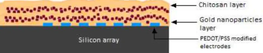
For this thesis, a combined coating of chitosan and gold nanoparticles was chosen, along with an microelectrode modification with PEDOT:PSS (Figure 4).
Figure 4 – Representation of the structural modifications on silicon microelectrode arrays. The process begins with the electrodes modification with PEDOT/PSS, followed by layer-by-layer coat-ing with chitosan and gold nanoparticles.
Improving Silicon Probe Performance Through Layer-by-Layer Coating
6
Materials and Methods
The experimental work evolved the preparation of several solutions and layer-by-layer and electrodeposition techniques to obtain the structural changes in the silicon probes. Posterior, morphological, electrochemical and in vivo characterizations were performed. In this chapter, all the solutions and techniques employed are explicit.
2.1 Solution-based synthesis
2.1.1 Chitosan
Chitosan composite (>75% deacetylation) was obtain from Santa Cruz Biotechnology. Chitosan solution (1% w/w) was prepared mixing distilled water with acetic acid (1% v/v).
2.1.2 Gold nanoparticles (AuNp’s)
The citrate reduction method was used to synthesize of gold nanoparticles. A solution consisting of 1 mM of tetrachloroauric acid (Sigma-Aldrich, 99.9%) was heated on a hot plate with a mag-netic stirrer until it reached the boiling point. To this solution, 1% (w/v) trisodium citrate (AnalaR NORMAPUR, 100%) was added and continuously stired. The solution was removed after it turn red from the hot plate. [26]
2.1.3 Poly(3,4-ethylenedioxythiophene) – Poly(styrenesulfonate) (PEDOT:PSS)
Synthesis of EDOT:PSS is obtained my mixing 0.01 M of EDOT (Sigma-Aldrich, 97%, MW = 142.18) in water and then add 0.1 M of PSS (Sigma-Aldrich, MW = 1000000), while stirred till the complete dissolution of EDOT.
2.2 AuNp’s Characterization
2.2.1 Dynamic Light Scattering (DLS)
Hydrodynamic diameter of gold nanoparticles in water was confirmed by Dynamic Light Scat-tering (DLS) technique (W130i Avid Nano).
Improving Silicon Probe Performance Through Layer-by-Layer Coating
7
2.3 Coatings Characterization
2.3.1 Atomic Force Microscope (AFM)
Chitosan/AuNp coating morphology was analyzed by atomic force microscopy (AFM, Asylum Research MFP-3D Standalone).
2.3.2 Scanning Electron Microscopy (SEM)
Chitosan/AuNp coating morphology was confirmed by scanning electron microscopy (SEM-FIB, Zeiss Auriga).
2.3.3 Contact Angle
The hydrophilicity of the Chi/AuNp coating was tested using Contact Angle System OCA (Data Physics).
2.4 Silicon Probes
Different silicon probes with distinct configurations were used:
- One shank: 32 iridium electrodes with a diameter of 15µm.
- Eight shanks: 4 iridium electrodes per shank - 32 in total – with a 20µm diameter. Additionally, silicon wafers were used and pieces of 1 x 2 cm were used for purposes of coat-ing’s degradation over time.
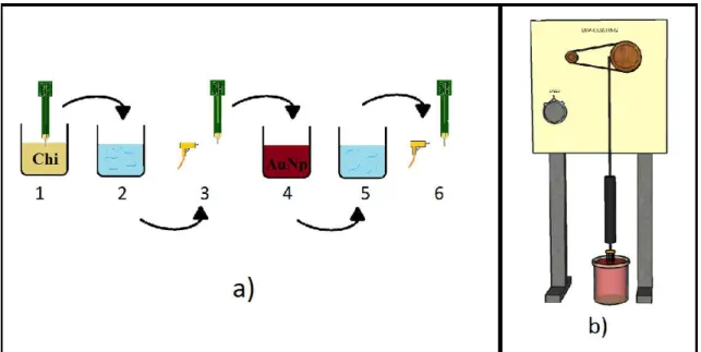
2.4.1 Dip-coating
Improving Silicon Probe Performance Through Layer-by-Layer Coating
8
Figure 5 – Dip-coating procedure. Schematics of the different steps that constitute the process: 1,4
– chitosan and gold nanoparticles solution; 2,5 – distilled water; 3,6 – nitrogen drying (a); Dip-coating mechanism representation (b).
2.4.2 Impedance characterization
A NanoZ (Neuralynx) system with two electrode cell configuration was used to measure the electrodes impedance at 1 kHz. The different probes were connected as working electrodes, whereas an Ag/AgCl wire (Science Products GmbH, E-255) was the reference electrode.
Improving Silicon Probe Performance Through Layer-by-Layer Coating
9
2.4.3 Morphological Characterization
Study of electrode structural modifications and coating was done by SEM (SEM-FIB, Zeiss Auriga) between 1 and 2 kV using a specific probe setup.
2.4.4 Electrodeposition Set-up
The PEDOT/PSS electrochemical depositions were performed using the NanoZ system repre-sented in Figure 5. A galvanostatic deposition process was used, where the previous chosen cur-rent is remained constant over time. The deposition is made targeting each electrode individual-ly, thanks to the software’s ‘Manual Control’.
2.5 Chronic Surgery
To analyze the coating’s performance in vivo an anesthetized male rodent (Long Evans) with about 500g was used. During the surgery the rodent was immobilized and receiving anesthetic isoflurane (1 L/min O2, 2% isoflurane), while the body temperature was constantly measured. The surgical procedure has its beginning with the rodent’s skin removal, leaving the targeted brain areas exposed. Then, using a rat brain atlas, the different landmarks on the skull are identi-fied, proceeded by two craniotomies (4 x 2 mm, one for each probe) and the consequent dura matter removal.
Two high density electrode silicon arrays (Poly3-25s, Neuronexus Technologies) were inserted via a micromanipulator that descends at a constant speed (1 µm/s). The probes (one with Chi/AuNp’s coating and one control) were located in the brain’s frontal lobe on both hemi-spheres, with an equal distance to its middle.
2.6 In vivo Recordings
Improving Silicon Probe Performance Through Layer-by-Layer Coating
10
2.7 Histological Characterization
Improving Silicon Probe Performance Through Layer-by-Layer Coating
12
Results
3.1 Coating Characterization
3.1.1 Pre-Surgery Impedance Characterization
In order to define the ideal number of total layers for the film, an impedance test compar-ing the electrodes impedance values between five layers and eleven layers total was carried out in two silicon probes with 32 electrodes. The five layers and eleven layers had three and six chi-tosan layers coated, respectively, with gold nanoparticles deposited in between. In Figure 7, it’s possible to observe a slightly increase in the impedance value for both probes, where the probe coated with five layers film experienced an impedance variation of around 12 kΩ (compared with 101 kΩ for the eleven layers probe – Table 1).
Figure 7 – Impedance variation after the deposition of the film for both probes. The probe coated with eleven layers total experienced a higher average impedance increase.
Improving Silicon Probe Performance Through Layer-by-Layer Coating
13
Table 1 – Average electrodes impedances and standard deviations for the probe with five and eleven layers coated.
Five layers film Eleven layers film Impedance Variation (kΩ)
± SD (
σ
)
11 ± 4 101± 22
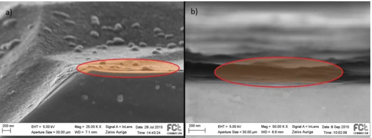
3.1.2 Morphologic Characterization
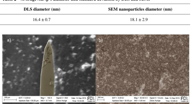
Coating’s morphology was analyzed via SEM and AFM. To compare the film’s thickness and roughness dependent on the number of layers coated, two silicon wafers were prepared with five and eleven layers in total. As expected, the silicon wafer coating with more layers deposit-ed presentdeposit-ed a superior thickness (200 nm, versus 40 nm, using ImageJ software), being also possible to observe a smoother surface compared with sample a) (Figure 8). The five layers total film provides then higher roughness, associated with a lower impedance magnitude, and so it was the film deposited for the chronic implanted probe. In figure 9 it is possible to observe the probe’s coating with five layers where a homogenous film that covers all the electrodes is pre-sented. This indicates the film’s good adhesion to the silicon probe. It is also presented the gold nanoparticles diameter measured by DLS and SEM (using ImageJ – Table 2).
The film’s color
was manually modified, as in the following images.
Improving Silicon Probe Performance Through Layer-by-Layer Coating
14
Table 2 –Average AuNp’s diameter and standard deviation by DLS and SEM.
Figure 9 – Silicon probe with chitosan/AuNp coating observed in SEM showing some dust parti-cles (a) and also some gold nanopartiparti-cles agglomerates (b).
In Figure 10, a more detailed study on the concentration of gold nanoparticles solution was car-ried out. For this study, AuNp’s solution was centrifuged for 30 min at 9000 rpm. The superna-tant was then removed and the remaining solution was used for silicon wafer coating (Figure 10 b), compared with the standard AuNp’s solution used in Figure 10 a). It’s possible to conclude that the average diameter of the structures formed by the gold nanoparticles is inferior in (a). This may be due to the higher concentration of nanoparticles, which tend to agglomerate in or-der to minimize the energy, whereas in (a) the nanoparticles are more dispersed. Despite the homogeneity in both solutions, the film in (a) presents more promising results compared with (b), due to a higher surface area and the inferior concentration of the solution used, leading to a smaller chance of nanoparticles released in the organism.
DLS diameter (nm) SEM nanoparticles diameter (nm)
Improving Silicon Probe Performance Through Layer-by-Layer Coating
15
Figure 10 - Coating morphology study via AFM. Both films have the same number of layers depos-ited, although in b) the gold nanoparticles solution used had a higher concentration compared to the one in a).
3.1.3 Contact Angle
In Figure 11, we can see the shape of a PBS drop in a silicon wafer with the Chi/AuNp five layers film coated, with a contact angle of 64.7 ± 2.1º for both sides of the drop (below 90º the solution is considered hydrophilic), which is close to the ones obtained in the literature [23]. The roughness and hydrophilic properties promote an enhanced adhesion between the coating and the surrounding cells. The contact angle obtained for an uncoated silicon surface was of 59.2 ± 1.2º.
Improving Silicon Probe Performance Through Layer-by-Layer Coating
16
3.1.4 Degradation Characterization
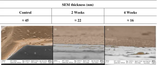
To test and analyze the 5 layers coating’s degradation over time, in order to foresee the probe’s performance in chronic implants, 2 different silicon wafers were placed inside a PBS solution (simulating the brain’s conditions) at 37 ºC over a month, being one removed after two weeks and the other one after four weeks. Another silicon wafer was left out with the purpose of serving as a reference. Via SEM, it’s possible to see that the coating’s thickness slowly decrea s-es over time, with the last silicon wafer coating having approximately one third the thickns-ess (≈16 nm) of the control one (≈45 nm). That said, we can conclude that the coating resists in simulated brain conditions over a month, despite the reduction in thickness, and so the biocom-patibility feature is expected to remain intact.
Table 3 - Average thickness obtained by SEM for the coating over a period of a month in PBS at 37 ºC.
SEM thickness (nm)
Control 2 Weeks 4 Weeks
≈ 45 ≈ 22 ≈ 16
Figure 12 - Degradation of the chitosan/gold nanoparticles coating on a 37 ºC PBS solution over time. First, the control silicon wafer a); coating after two weeks b); coating after four weeks c).
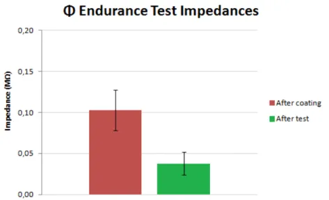
3.1.5 Endurance Test
Improving Silicon Probe Performance Through Layer-by-Layer Coating
17
impedance can then be explained with remains of agar still attached to the probe, despite the rinsing that was carried out.Figure 13 – Variation of the average impedance magnitude for 28 electrodes (at 1 kHz) after coat-ing deposition (red) and after endurance test with agar (green).
3.2 In vivo Recordings
In chronic surgery we aimed to evaluate the performance differences between an un-coated and a un-coated silicon probe, both with respect to level of inflammatory response and qual-ity of the recording signal. For that purpose, two silicon microelectrode arrays probes were in-serted in a rodent’s brain, both modified with PEDOT:PSS but only one with chitosan/AuNp film coating. Due to the imminent fall of the implants, there was need for an early perfusion of the rodent, and so the duration of the experiment was of three weeks instead of the four initially planned.
3.2.1. Electrodes Impedances
Improving Silicon Probe Performance Through Layer-by-Layer Coating
18
Figure 14 - Variation of the average impedance magnitude (at 1kHz) for the two chronic sur-gery selected probes. Impedances for probe 1, before and after the electrodeposition of PEDOT:PSS (a); Results obtained before and after PEDOT:PSS, and also after the deposition of the chitosan/AuNp coating (b).
Improving Silicon Probe Performance Through Layer-by-Layer Coating
19
The impedance variation for the probe coated with the Chi/AuNp film is then significant-ly inferior to the ones obtained for the uncoated probe, presenting strong evidence that the coat-ing provided a biocompatible tissue that led to a reduction of the organism inflammatory re-sponse. This evidence is also supported by the detection of numerous and regular neuron spikes by the coated probe (results that together with the histology tests will be presented further on in this work). Relying in previous recording experiments performed on lab, electrodes with imped-ances above 2MΩ implied low signal to noise ratio being hard to detect spikes. Due to the in-flammatory response already discussed, there was an increase in the electrodes impedances in both implanted probes, with the uncoated probe presenting a significant increase compared with the coated probe (this led to the inability to detect any neuron spiking activity with the uncoated probe, as it is demonstrated further on). The measured impedances experienced an increase over the three weeks experiment [27]. This can be explained by the agglomeration of immune system cells around the probes, leading to a further detachment between the recording electrodes and the nearby neurons.Improving Silicon Probe Performance Through Layer-by-Layer Coating
20
Figure 16 – Electrodes impedance variation for the coated probe, with a peak of 0.74 ± 0.4
MΩ at the end of the experiment.
3.2.2. Neurons Spikes
Throughout the chronic implantation, the rodent was connected to the acquisition board and the neurons spikes captured by the electrodes were measured and analyzed. To compare the performance between both probes, a single electrode (number 22) was chosen and the spikes detected were examined in terms of number of spikes and their average amplitude (Figure 17).
Improving Silicon Probe Performance Through Layer-by-Layer Coating
21
Improving Silicon Probe Performance Through Layer-by-Layer Coating
22
3.2.3. Biocompatibility Characterization
To evaluate the organism inflammatory response, a conventional histology by hematoxylin and eosin staining of the rodent brain slices was carried out. The H&E staining enabled the visualization and differentiation of the diverse cells that constitute the immune re-sponse, allowing a comparison between the wounds caused by the implant of both probes.
After three weeks, the acute immune reaction already took place and it is followed by a chronic inflammatory response, characterized by the presence of glial cells such as lymphocytes and plasmocytes around the implants lesions (marked in Figure X). It is visible the superior number of these cells around the lesion caused by the uncoated probe when compared to the coated one, and so it is possible to conclude that the deposition of the biocompatible film lead to a reduced inflammatory response by the organism.
Improving Silicon Probe Performance Through Layer-by-Layer Coating
24
Conclusions and Future Perspectives
This project proposed structural modifications of silicon probes in order to reduce the implants immune inflammatory response, as well as improving the electrical signal recorded from the microelectrodes. For that purpose, a combined coating of chitosan and gold nanoparti-cles was produced, associated with microelectrodes modifications by galvanostatic electrodeposition of PEDOT/PSS. These structural modifications were studied and tested before a chronic surgery, with the inflammatory response and electrical recording results along and after the surgery being presented also.
A film constituted by five layers of chitosan and gold nanoparticles combined was de-posited in silicon microelectrode arrays by dip-coating process. The coating presented great morphological and electrochemical properties pre-surgery, with an increase in average elec-trodes impedance of 7 kΩ and an average thickness of 50 nm, being also characterized by some roughness and a contact angle of 64.7 º. The gold nanoparticles were distributed along the film, with an average diameter of 16 nm. The PEDOT/PSS electrodes modifications proved to be an efficient and reliable method to diminish the electrodes impedance, reducing it on a scale of some hundreds of kΩ.
To test the coating’s behavior in chronic surgery, a three week experiment was pe r-formed on a rodent (Long Evans). Two probes were implanted, one with only the electrodes modifications using PEDOT/PSS and another one with the Chi/AuNp film coated on top of the modified electrodes. Both probes performances were evaluated in terms of impedance variation, detection and characterization of neuron spikes and histological tests. With an initial average value of 0.122 ± 0.1 MΩ, the electrodes impedances for the uncoated probe at the end of the experiment were of 2.538 ± 0.9 MΩ, reaching values that turn the probe unusable to detect and record neural activity. However, for the coated probe the final impedance value was of 0.735 ± 0.4 MΩ, allowing the recording of numerous spikes and their respective characterization. The coating of Chi/AuNp in conjunction with the electrodes modifications by PEDOT/PSS presents then an efficient solution to improve the silicon probes performance in chronic implants to at least one month.
Spontaneous neuronal activity was detected and recorded by both probes. On the acute recordings, both probes performed well, detecting several and ample neurons spikes (only one electrode was analyzed for both probes, electrode number 22). However, as the experiment ran through, the differences between both probes performance became more apparent, sustained by
Improving Silicon Probe Performance Through Layer-by-Layer Coating
25
the results obtained half-way through and at the conclusion of the experiment, where the un-coated probe was unable to detect any significant neuron spikes (the un-coated probe continued to detect spikes, with an average amplitude of 281 µV).A histological characterization of rodents brain cells allowed the detection and visuali-zation of a minor chronic inflammatory response for both probes wounds. Nevertheless, the sig-nificantly superior number of glial cells around the uncoated probe wound, when compared with the coated one, suggests that the deposition of the biocompatible film along with the electrodeposition of PEDOT/PSS on the probe reduced the organism immune response.
As for future perspectives, for a deeper study in how the deposition of a biocompatible coating affects the probe’s performance in chronic implants, further surgeries need to be pr e-pared regarding the deposition of this five layers film, comparing the results between a coated and an uncoated probe for an extended period of time (4-6 months for example). The variation of the diverse properties of the coating, such as thickness or the solutions concentration, should also be tested, enabling a comparison between the different deposited coatings performance in rodents chronic implants.
Improving Silicon Probe Performance Through Layer-by-Layer Coating
26
References
[1]
S. F. Cogan, “Neural stimulation and recording electrodes.,”
Annu. Rev. Biomed.
Eng., vol. 10, pp. 275
–
309, Jan. 2008.
[2]
R. Mukamel and I. Fried, “Human Intracranial Recordings and Cognitive
Neuroscience,”
Annu. Rev. Psychol., vol. 63, no. 1, pp. 511
–
537, 2012.
[3]
M. Seeck, F. Lazeyras, C. M. Michel, O. Blanke, C. A. Gericke, J. Ives, and J.
Delavelle, “Non
-invasive epileptic focus localization using EEG-triggered
functional MRI and electromagnetic tomography,”
Electroencephalography and
Clinical Neurophysiology, vol. 106, pp. 508
–
512, 1998.
[4]
V. S. Polikov, P. a. Tresco, and
W. M. Reichert, “Response of brain tissue to
chronically implanted neural electrodes,”
J. Neurosci. Methods, vol. 148, no. 1,
pp. 1
–
18, 2005.
[5]
R. J. Vetter, J. C. Williams, J. F. Hetke, E. a. Nunamaker, and D. R. Kipke,
“Chronic neural recording using silicon
-substrate microelectrode arrays
implanted in cerebral cortex,”
IEEE Trans. Biomed. Eng., vol. 51, no. 6, pp. 896
–
904, 2004.
[6]
S. Take
uchi, D. Ziegler, Y. Yoshida, K. Mabuchi, and T. Suzuki, “Parylene
flexible neural probes integrated with microfluidic channels.,”
Lab Chip, vol. 5,
no. 5, pp. 519
–
523, 2005.
[7]
J. Zhang, F. Laiwalla, J. a Kim, H. Urabe, R. Van Wagenen, Y.-K. Song, B. W.
Connors, F. Zhang, K. Deisseroth, and A. V Nurmikko, “Integrated device for
optical stimulation and spatiotemporal electrical recording of neural activity in
light-
sensitized brain tissue.,”
J. Neural Eng., vol. 6, no. 5, p. 055007, 2009.
[8]
J. C. Sanchez
, N. Alba, T. Nishida, C. Batich, and P. R. Carney, “Structural
modifications in chronic microwire electrodes for cortical neuroprosthetics: A
case study,”
IEEE Trans. Neural Syst. Rehabil. Eng., vol. 14, no. 2, pp. 217
–
221,
2006.
[9]
M. HajjHassan, V. Cho
davarapu, and S. Musallam, “NeuroMEMS: Neural Probe
Microtechnologies,”
Sensors, vol. 8, no. 10, pp. 6704
–
6726, Oct. 2008.
[10]
B. Y. D. E. Goldman, “IN MEMBRANES ( From the Department of ]
Physiology , College of Physicians and Surgeons , Columbia University , New
York ) The Journal of General Physiology,” pp. 37–
60, 1943.
[11]
T. F. Chan and J. Shen, “Image processing and analysis: variational, PDE,
wavelet, and stochastic methods,”
Book, no. October 2015, p. 400, 2005.
[12] G. Buzsáki, C. a. Anastassiou,
and C. Koch, “The origin of extracellular fields
and currents
—
EEG, ECoG, LFP and spikes,”
Nat. Rev. Neurosci., vol. 13, no.
6, pp. 407
–
420, 2012.
Improving Silicon Probe Performance Through Layer-by-Layer Coating
27
[13] A. P. Alivisatos, A. M. Andrews, E. S. Boyden, M. Chun, G. M. Church, K.
Deisseroth, J. P. Donoghue, S. E. Fraser, O. J. Lippincott-schwartz, L. L. Looger,
S. Masmanidis, P. L. Mceuen, A. V Nurmikko, H. Park, D. S. Peterka, C. Reid,
M. L. Roukes, A. Scherer, M. Schnitzer, T. J. Sejnowski, K. L. Shepard, D. Tsao,
G. Turrigiano, P. S. Weiss, C. Xu, O. O. R.
Yuste, and X. Zhuang, “Nanotools
for Neuroscience and Brain Activity Mapping,”
ACS Nano, vol. 7, pp. 1850-66,
2013.
[14] F. Franke, D. Jäckel, J. Dragas, J. Müller, M. Radivojevic, D. Bakkum, and A.
Hierlemann, “High
-density microelectrode array recordings and real-time spike
sorting for closed-loop experiments: an emerging technology to study neural
plasticity,”
Front. Neural Circuits, vol. 6, no. December, pp. 1
–
7, 2012.
[15] S. Venkatraman, J. Hendricks, S. Richardson-Burns, E. Jan, D. Martin, and J. M.
Carmena, “PEDOT coated microelectrode arrays for chronic neural recording
and stimulation,”
2009 4th Int. IEEE/EMBS Conf. Neural Eng. NER ’09
, vol. 4,
pp. 383
–
386, 2009.
[16] S. J. Wilks, S. M. Richardson-burns, J. L. Hendricks, D. C. Martin, and K. J.
O
tto, “Poly ( 3 , 4
-ethylenedioxythiophene ) as a micro-neural interface material
for electrostimulation,”
Front Neuroengineering
, vol. 2, no. June, pp. 1–
8, 2009.
[17] K. a Ludwig, N. B. Langhals, M. D. Joseph, S. M. Richardson-Burns, J. L.
Hendricks, and
D. R. Kipke, “Poly(3,4
-ethylenedioxythiophene) (PEDOT)
polymer coatings facilitate smaller neural recording electrodes.,”
J. Neural Eng.,
vol. 8, no. 1, p. 014001, 2011.
[18]
W. Franks, I. Schenker, P. Schmutz, and A. Hierlemann, “Impedance
characterizatio
n and modeling of electrodes for biomedical applications,”
IEEE
Trans. Biomed. Eng., vol. 52, no. 7, pp. 1295
–
1302, 2005.
[19]
R. Biran, D. C. Martin, and P. a Tresco, “Neuronal cell loss accompanies the
brain tissue response to chronically implanted silic
on microelectrode arrays.,”
Exp. Neurol., vol. 195, no. 1, pp. 115
–
26, Sep. 2005.
[20] J. N. Turner, W. Shain, D. H. Szarowski, M. Andersen, S. Martins, M. Isaacson,
and H. Craighead, “Cerebral astrocyte response to micromachined silicon
implants.,”
Exp. Neurol., vol. 156, no. 1, pp. 33
–
49, 1999.
[21] K. E. Crompton, J. D. Goud, R. V. Bellamkonda, T. R. Gengenbach, D. I.
Finkelstein, M. K. Horne, and J. S. Forsythe, “Polylysine
-functionalised
thermoresponsive chitosan hydrogel for neural tissue engineering,
”
Biomaterials,
2007.
[Online].
Available:
https://neurolab.gatech.edu/wp-
content/uploads/bellamkonda/publications/2007-01_crompton_goud_bellamkonda_gengenbach_finkelstein_horne_forsythe.pdf.
[Accessed: 16-Feb-2015].
[22]
H. Yang, S. Zhou, and X. Deng, “Pr
eparation and Properties of Hydrophilic
–
Hydrophobic Chitosan Derivatives,”
Journal of Applied Polymer, no. May, pp.
1625
–
1632, 2004.
[23] J. D. Bumgardner, R. Wiser, S. H. Elder, R. Jouett, Y. Yang, and J. L. Ong,
Improving Silicon Probe Performance Through Layer-by-Layer Coating
![Figure 1 - Various systems configurations for neural study. Single tungsten wire without modifica- modifica-tions (a) [8]; Michigan probe, a silicon based neural probe with 1024 electrodes (b); Flexible probe array constituted by polyimide (c) [9];](https://thumb-eu.123doks.com/thumbv2/123dok_br/16694675.743774/24.892.222.671.122.519/various-configurations-tungsten-michigan-electrodes-flexible-constituted-polyimide.webp)