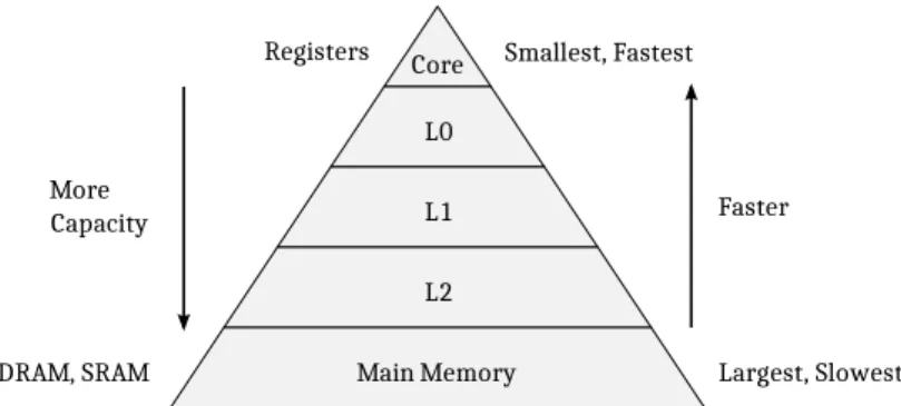
Because of the performance gap between processor and memory, instruction memory hierarchy design is a mandatory part of processor designs. The memory hierarchy not only helps maintain performance, but also affects the power consumption of large memory. In this thesis, custom memory hierarchy generation was implemented and integrated into the TTA-based Co-design Environment (TCE) processor generator developed at Tampere University of Technology.
The generator reads the instruction memory hierarchy description and constructs a TTA-based processor that includes the specified hierarchy.
INTRODUCTION
This includes tool-assisted generation of a custom instruction memory hierarchy and tools to verify and collect performance statistics from it. Working implementations have been integrated into the TTA-based Co-design Environment (TCE) [2] where memory hierarchy generation has been requested. TCE covers the development of the component aspect of the data path, but lacked the customization of instruction memory hierarchies.
This thesis is divided into chapters as follows: Chapter 2 gives the background of custom processors the part that is relevant to instruction memory hierarchies.
CUSTOMIZED PROCESSORS
Transport Triggered Architecture
- Processor Organization
- Programming Model
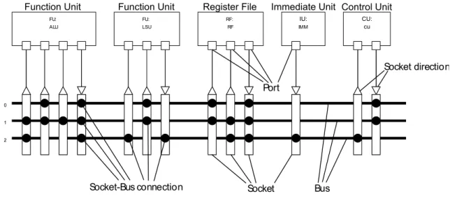
Data paths of a TTA processor are visible and controllable; which allows programmers and compilers to use data bypasses and thus reduce RF usage. Different types of TTA units are function unit (FU), register file RF, control unit and Immediate Unit (IU). For example, in figure 2.1, arithmetic logic unit (ALU) performs basic arithmetic operations and load storage unit (LSU) accesses data memory.
The control unit (CU) is a special case of the FU and controls the flow of programs executed in the TTA processor and is responsible for receiving instructions.
TTA-based Co-design Environment
TCECC and TCE assembler TCECC is a retargetable compiler for compiling TTA programs from high level languages - such as C/C++. The simulator can simulate any operation in the machine through Operation Set Abstraction Layer (OSAL). Users can define their own operations, which can then be used in the TTA simulations.
In this thesis, the data extracted from TTAsim is used in verification and for the automated generation of test cases.
INSTRUCTION MEMORY HIERARCHIES
Instruction Cache
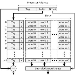
The tag and the valid bit together determine whether a requested instruction is present in the cache. Since a block can consist of many words, the lower parts of the address are used to select the required word. The basic cache data structure is formed by a set of block entries, a label and a value bit.
If the valid bit in the entry indicates false, then it is clear that the requested word is not in the cache.
Bus Arbiter
PROCESSOR GENERATION IN TCE
Processor Generator
- Processor Generation Flow
- Instruction Pipeline
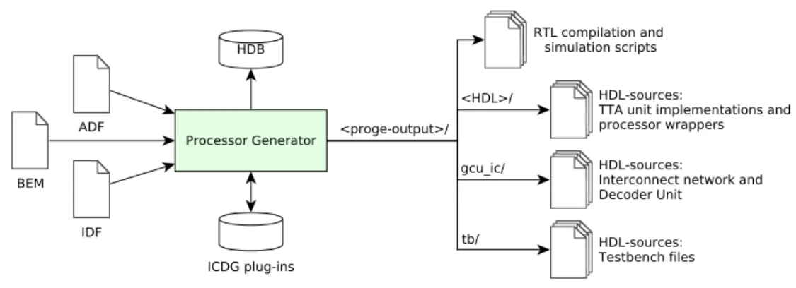
What is excluded from ADF are the actual implementation details of the processor - the micro-architecture. The creation of the IC and instruction decoding unit is delegated to the Interconnect Generator and Decoder (ICDG) plug-in. ProGe calls the ICDG-plugin, which completes the processor core template by adding dynamically generated ICs and the instruction decoder unit and selecting the implementation for the instruction fetch unit.
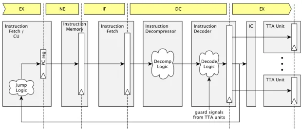
Figure 4-2 shows the structure of the instruction pipeline generated by default in ProGe. There are a number of fetch unit types provided by TCE: a normal fetch unit that fetch fixed size instructions and another that fetch variable length instructions [15]. In both types, the width of the fetch block is fixed, but with the last fetch unit type, a single fetch block can have zero or more instructions.
The fetch unit expects the instruction memory to provide data from the given address when memory enable signal is active. If the memory cannot respond (in time) to the request, it can fetch the instruction by asserting a busy signal. The retrieval unit is the control unit in TTA machines and therefore handles control operations connected to it.
The process of retrieving data from instruction memory and converting it into control signals takes several cycles. The pipeline latency visible in ADF and in TTA program code is represented as delay slots after control flow operations.
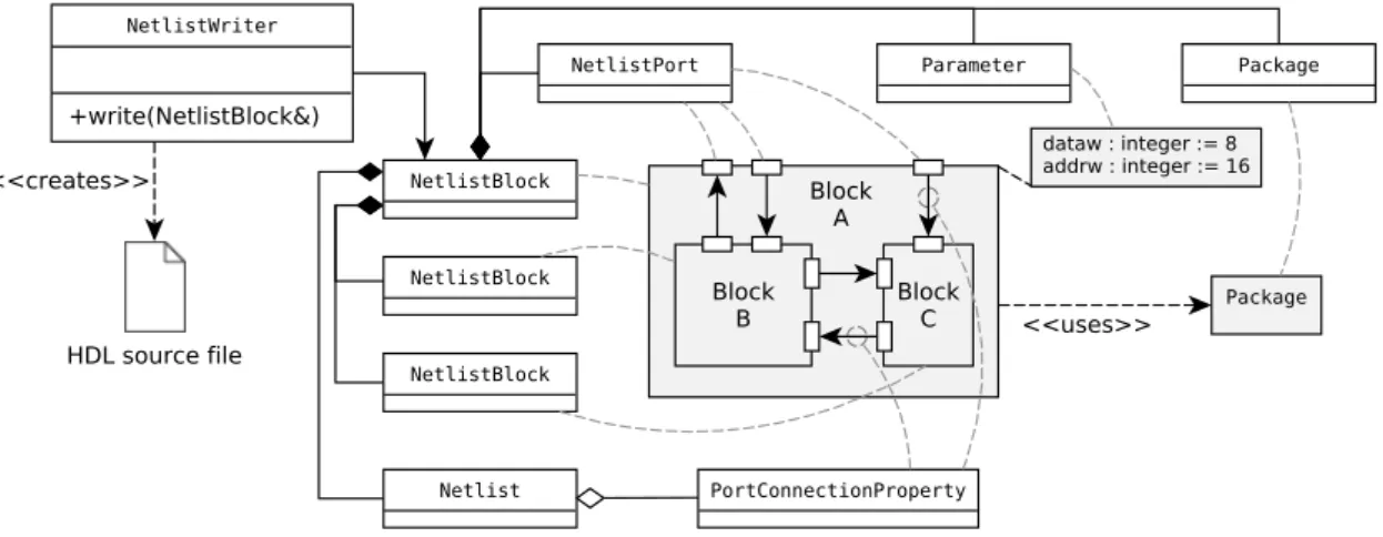
Netlist Module
Figure 4.4 presents the basic classes used to model hardware structures. Netlist blocks are created to model the implementation source files - those stored in the HDB and internal library. The netlist writer reads the block-level netlist structure and creates an HDL source file behind it.
The netlist classes provide enough information so that netlist writers can write valid HDL resources that successfully instantiate other blocks and make connections. Table 4.1 shows how class module maps to Verilog and VHDL language attributes. Isolated Netlist Blocks Objects of the NetlistBlock class can be freely modified - ports, parameters, subblocks and internal connections can be added, modified and recreated.
Netlist module 17 Table 4.1 Netlist classes and their rough correspondence to those in the HDL languages Verilog and VHDL. This makes the class unsuitable for deriving specialized netlist block classes that would need limited capabilities. The netlist module was changed so that all netlist block classes are derived from the BaseNetlistBlock class that have no public modifier methods.
In the new way, the netlist block classes have an overridable write() function that allows specialized netlist blocks to write HDL sources on their own. Hierarchical Netlist Structure In principle, the old Netlist module could model hierarchical block structures - blocks that have sub-blocks that have sub-blocks and so on.
CONFIGURABLE LOOP BUFFER
- Setup Operation and Operation Principle
- Usage in Program Code
- Using Loop Buffer in Design
- Hardware Implementation
- Integration
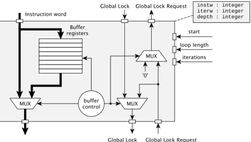
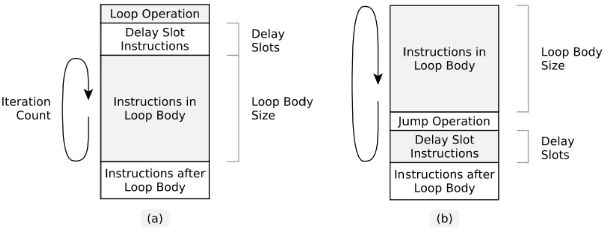
In Program Listing 5.1, there is an example of a TCE assembly code snippet that uses a loop buffer. The remaining behavior of the loop buffer operation is implemented in the loop buffer unit. The start signal triggers the loop buffer using the other two as arguments to the loop.
Also, global lock and global lock signals are bypassed and do not affect the loop buffer. After the first iteration of the loop, the loop buffer blocks the upper part of the instruction pipeline by asserting the global block request signal (Figure 5.5: c). The request for global latching signals and global blocking affects the loop buffer only when it is enabled.
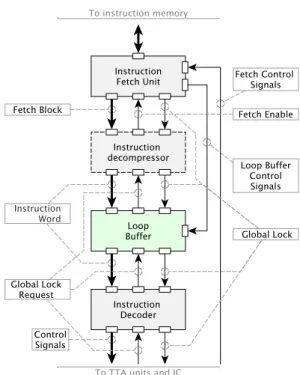
A loop buffer is automatically created if the ADF describes a loop buffer operation within the CU. The actual loop buffer HDL source file is copied to the processor target directory. The loop buffer parameters (buffer depth and iteration gate width) are provided in the TTA processor globals package.
The loop buffer is controlled by an instruction fetch unit which is the forefront of CU. The control logic of the loop buffer is injected into the instruction fetch unit in this manner.
INSTRUCTION MEMORY HIERARCHY GENERATIONGENERATION
- Instruction Memory Hierarchy Customization
- Instruction Cache
- Implementation Details
- Instruction Arbiter
- Integration into ProGe
- Implementation of Cache Statistics Collection
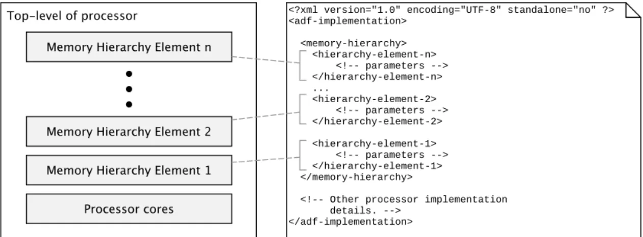
HDL description of the instruction memory hierarchy is generated by ProGe using the description in IDF. Thereafter, the processor generator proceeds to construct the defined memory hierarchy by creating netlist models from the hierarchy elements, which are placed at appropriate locations in the processor netlist model. Cached blocks are distributed and stored under one or more memory blocks, depending on the set block size and width of the memory blocks.
This means that the instruction bus to memory can be the width of the block or be smaller than the instruction size. The controller generates only the lower part of the addresses (i in the equation) and they are combined with block start address calculated in the upper level. A use case of the feature is in program loading, where invalidating the cache is needed to discard blocks belonging to an old program.
As in the Figure 6.7, the loop buffer and level 1 instruction cache are instantiated in TTA core netlist block. In the Figure 6.8 is Netlist Block FlexSoCCache class presentation of the level 1 instruction cache model introduced earlier in section (6.2). The L1 cache parameters themselves are packaged in L1CacheParameters object which is a representation of the level 1 instruction cache parameters defined in .
The tool also shows the total number of final instruction memory accesses made from the processor. Some of the dump files, for cache statistics, are access traces, which tell about memory access events made in cache and memories in the processor.
VERIFICATION
- Automated Test Generator
- Usage
- Test Generation Framework
- TTA Processor Test Bench Improvements
- Test Environment
- Loop Buffer Verification
- Memory Hierarchy Generation
- Instruction Cache Test Case Generation
- Verification
TPEF is intended to debug the TTA simulator in case the test case fails in the RTL simulation. Many tests generated in TeGe are pseudo-random, but the generation is deterministic. The test runner script (testrunner.py) is a utility that runs all generated test cases (in program image format) in an RTL simulation and reports whether the test cases are successful or not.
Test cases are created by running test generator by providing ADF and IDF of the processor. The TeGe creates test cases for FU operations found in the processor, and by default it creates tests for the operations by generating random inputs. The inner workings of the test generator are depicted in Figure 7.2, which is a class diagram of TeGe's framework.
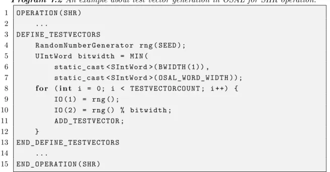
A basic implementation of the makeTestVectors() function in OperationBehavior pseudo-randomizes a series of test vectors. RTL simulations are used to extract cache and power consumption statistics by running various test programs in the generated processors. For this, the RTL simulation time must be limited to the duration of the test program.
One solution was to create the processor test suite to trace program execution on the TTA processor and dynamically stop the simulation when the instruction count limit is reached. HDL code coverage is used to provide feedback on test scope. Tables 7.6, 7.7 and 7.8 show the average power ratings and total processor power consumption.
The verification was performed by changing the core count of the processor and forcing processor to halt.
FUTURE WORK
RELATED WORK
CONCLUSION
BIBLIOGRAPHY
24] Shyamkumar Thoziyoor, Naveen Muralimanohar, Jung Ho Ahn and Norman Jouppi. CACTI: Integrated cache and memory access time, cycle time, area, leakage and dynamic power model.