It was an honor and a privilege to work with him on the current thesis. Finally, the chapter concludes with an overview of the contributions of the current text.
Context
In the "predictable" world of digital systems governed by clocks, synchronization, (dead) lock and deadlines, variability is usually the culprit of misbehavior. In the current text, reactive power augmentation is proposed to mitigate performance variability (Chapter 6).
![Figure 1.1: Transistor downscaling trends [258]](https://thumb-eu.123doks.com/thumbv2/pdfplayerco/303122.42324/32.680.82.592.305.856/figure-1-1-transistor-downscaling-trends-258.webp)
Reliability Background
Reliability analysis of a digital system is the monitoring of system performance in the presence of reliability violations. Monitoring the system during reliability analysis can address functional and parametric reliability violations with varying degrees of severity.
![Figure 1.2: The chain of events from a physical mechanism to a system- or user-perceived failure [231]](https://thumb-eu.123doks.com/thumbv2/pdfplayerco/303122.42324/34.680.87.591.103.239/figure-chain-events-physical-mechanism-user-perceived-failure.webp)
Functional vs. Parametric Reliability Violations
This is a far less complex procedure than statistically handling the observed values to resolve the extent of the parametric reliability violation and infer the underlying distributions. From the above, it is clear that parametric reliability violations at the circuit level cause functional ones at the register transfer level (RTL).
Contributions and Text Structure
Injection
A HW description is executable and in our case allows changes to inject reliability violations. Also, a simulation/emulation tool that outputs the HW description could be improved to allow injection of reliability violations.
Detection
Reliability Modeling
Environment-Inherent Reliability Violations
If the adjacent system is not functionally connected to the system under test, disturbances that can be examined may require a conductive path. If the natural environment is uncorrelated with the system under test, a further distinction can be made based on whether a conduction path is required for the natural disturbance to reach the underlying digital system.
Platform-Inherent Reliability Violations
In the majority of heat transfer modeling papers, it is the neighboring HW that creates the extreme temperatures. When the use of the HW is coupled or configurable by the user, we evaluate both themapping tools[273].
Parametric Mitigation Within Package
Single Die
Multiple Dies
In relation to multiple integration, we can look at the connection of cables at different levels or the assembly procedure itself. With regard to the stacking of diapauses (regardless of forwarding links), we distinguish between tuning (i.e., setting the functionality of each layer level) and these choices.
Parametric Mitigation Across Packages
Hardware Solutions
General purpose techniques are divided between those referring to the processing components of the node [222] and those related to theme memory [188, 87]. Thermal stress of motor control modules is discussed by Kumar et al., with an emphasis on heat dissipation options and copper thickness of the printed circuit board (PCB) [148].
Software Solutions
The thermal headspace and package-enabled dissipation capabilities of on-board flight entertainment computer nodes are discussed by Sarno et al. Thermal limits of discrete components for electric traction drive systems (ETDSs) are presented by Moreno et al.
Overview of Representative Groups
One of the most important contributions of this group [272], which is very related to RAS costing as presented in the present text, is the RAZOR processor [75]. One of the most notable examples of is the reliability model Reliability-Aware MicroProcessors (RAMP) [217].
Current and Future Reliability Needs
Similarly, in the field of high-performance computing (HPC), the performance impact of resilience techniques has already been documented and formulated for the case of the Tianhe2 supercomputer [288]. Finally, system availability has been addressed as a resource management problem in the context of the 2PARMA project [7].
Critical Appreciation and Contributions
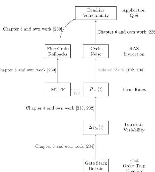
The core of the work presented in Chapter 3 was previously disclosed by the author in an IEEE TDMR journal article [234]. The core of the work presented in Chapter 4 was previously revealed by the author in two workshops [233, 232].
The Atomistic BTI Model
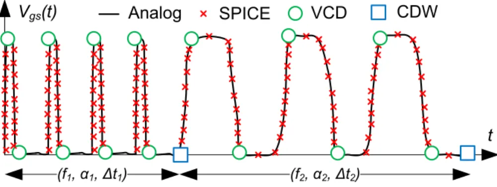
This option is clearly dependent on the workload, as 𝑃𝑐 is a function of the duration of constant voltage levels (𝑡𝑖). To calculate𝑃𝑐after 𝑛 digital pulses have been applied to the gate of the device, equation 3.3 is used, where constants𝑎and𝑏are functions of𝑓 and𝛼properties of the𝑉𝑔𝑠pulse series. As such, the CET map-based methodology is left outside the scope of the current text.
Proposed Tool Support
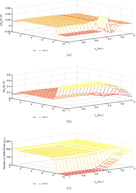
We determine the approximation error of the signal according to equation 3.6 and produce the mean values (Figure 3.4a) and standard deviation (Figure 3.4b). Given that wavapproxbuffer averages the values 𝑓 and In Figure 3.4c we see the number of points produced for different choices of error margins𝜀𝑓 and𝜀𝛼.
CDW Verification for BTI Modeling
Each iteration of the general solution of Equation 3.7 is used as initial condition for the next model evaluation. Given the compression capabilities of the CDW representation (see Figure 3.4c), the number of model iterations is aggressively reduced, thus. Given the proposed model of Equation 3.7, we will evaluate the accuracy of a CDW approach in terms of 𝑃𝑐 evaluation.
Thermal & Bias Applicability
Therefore, the time constants must be scaled appropriately before the error occupancy is resolved (see Figure 3.8). With a short simulation covering "fast" time constants, we get the short-term impact of the errors in question (Figure 3.11a). For the long-term impact of BTI/RTN, we create a CDW representation of device lifetime (up to 108 s) using 100 points.
![Figure 3.8: Before resolving occupancy of defects with the CDW, time constants need to be scaled [234]](https://thumb-eu.123doks.com/thumbv2/pdfplayerco/303122.42324/79.680.141.548.97.455/figure-resolving-occupancy-defects-cdw-time-constants-scaled.webp)
Design Flow Compatibility
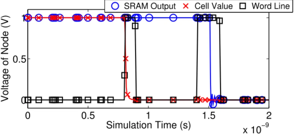
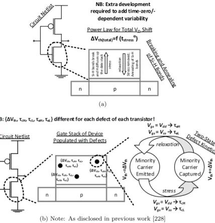
For the sake of brevity, we have ignored the influence of "fast" defects in the functional yield analysis. A defect-centered model, namely a simplified version of the previously discussed atomistic version BTI [41], has been used to capture time-zero and time-dependent variability in simple circuit operating parameters [280]. Estimating the failure probability of an SRAM cell can be performed in various ways.
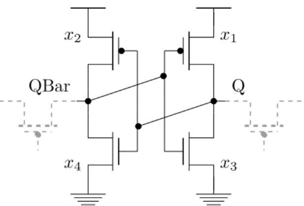
![Table 3.1: Atomistic model configuration for yield analysis of the target SRAM circuit, according to BTI/RTN measurements [265] and the 90 nm Predictive Technology Model [1], as initially disclosed in [234]](https://thumb-eu.123doks.com/thumbv2/pdfplayerco/303122.42324/85.680.86.598.101.252/atomistic-configuration-according-measurements-predictive-technology-initially-disclosed.webp)
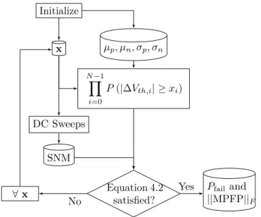
The MPFP Methodology
Regardless of the failure calculation method 𝑃, SRAM cell parameters can vary for many reasons: Zero-time variations are static and are the result of imperfect manufacturing [203]. The probability corresponding to each failure point is calculated based on the statistics of the parameters involved 𝑉𝑡ℎ. During exploration, for a given value of 𝑥𝑖, the equivalent probability is equal to the area highlighted in Figure 4.3, which is equal to
BTI Variability Models
Time-Zero Variability
Time-Dependent Variability and Aging
In other words, the average 𝑉𝑡ℎ aging of a transistor array follows a trend similar to the power law of Equation 4.6. Therefore, according to the defect-centered model, two identical transistors subjected to the same operating conditions may age differently. Recent defect-focused literature documents that, for devices with reduced resolution, the average displacement 𝑉𝑡ℎ caused by the BTI follows a power law similar to Equation 4.7 [143].

Simulation Flow and Results
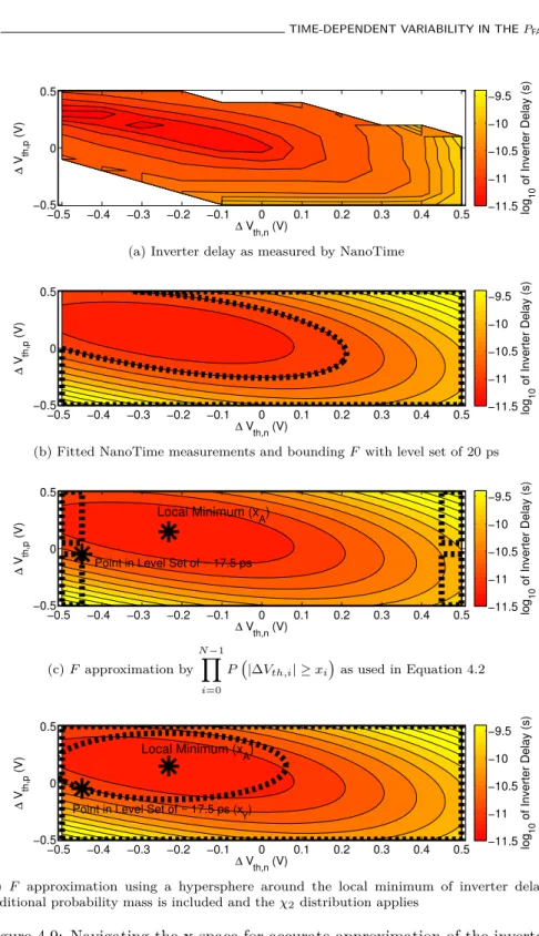
In Figure 4.6 we further focus on the 𝑃error benefit achieved by increasing the 𝑉𝑑𝑑 from 0.6 V to 0.7 V. Conversely, in Figure 4.7b both the mean and the standard deviation of the total𝑉𝑡ℎshift are functions of time. Given our observation about the 𝑃fail sensitivity to the standard deviation of the 𝑉𝑡ℎshift (Figure 4.5), we evaluate the 𝑃fail over a.
Discussion and Extensions to SSTA
Reformulating the MPFP – Inverter Case Study
In the case of the inverter, it is reasonable to expect a unique solution to this optimization problem. It is important to note that the above statement is correct regardless of the shape of 𝑦(x). This means that the inverter delay distribution has no tail on the left.
Background
Especially in cases where the scope of redundancy is almost global across the entire hardware, as in the case of Field Programmable Gate Arrays (FPGAs) [124], the associated area and power overheads are highly unacceptable. This introduces a temporary overhead, as in the case of transferring a value from memory (where it is protected) to the register file (where it is vulnerable). The current chapter focuses on memories and uses a many-core chip so that the overhead of inter-core communication is taken into account within the mitigation scheme [223].
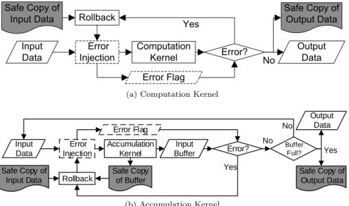
Rollback-Based Transient Error Mitigation
In this image processing application, the collection and computation cores (CK and AK) can be identified as shown in Figure 5.1a. An illustration of an OFDM transmitter using AK and CK can be seen in Figure 5.1b. In the context of aCK, we can mitigate a transient error in the data plane by keeping a safe copy of the input data and repeating the erroneous computation (illustrated in Figure 5.2a).
Experimental Setup
Target Platform
For the demonstration of the hybrid (HW-SW) mitigation technique presented in Section 5.2, a real SCC chip is used. It is important to consider the suitability of the SCC for illustrating the proposed HW-SW transient error mitigation technique. This is an important requirement for the proposed mitigation methodology, as outlined in section 5.2 and in previous work [236, 42].
Error Injection & Application Correctness
However, we refrain from "judged or hypothesized cause" [17] of injected errors (i.e. relevant fault). The display intensity DUE is measured in FIT and, in the context of this work, corresponds to the data cache of each of the SCC cores (see Figure 5.6a). If 𝑟 < 𝑃𝑒, we assume that an error has occurred and a random bit shift is applied to the corresponding kernel data.
![Figure 5.5: Schematic overview of the SCC layout and of our experimental setup [230]](https://thumb-eu.123doks.com/thumbv2/pdfplayerco/303122.42324/121.680.82.598.96.469/figure-schematic-overview-scc-layout-experimental-setup-230.webp)
Rollback Mitigation per Execution Node
A safe copy of the constants for the YUV to RGB transformation is created at the beginning of the execution. The above concept is repeated for each MCU in the frame and is depicted in Figure 5.7c. The reason is that, apart from output fidelity, we need to respect the time constraints of the application.
![Figure 5.7: Second step of the methodology: implementing the rollbacks on demand for every encountered kernel type [230].](https://thumb-eu.123doks.com/thumbv2/pdfplayerco/303122.42324/125.680.92.591.140.306/figure-second-methodology-implementing-rollbacks-demand-encountered-kernel.webp)
Experimental Results
Building the Pareto Space
Willingly ignoring injected DUEs for a portion𝑘WI (%) of the run recovers application loss but increases average frame distortion. Since both buttons are quantized as portions of the execution, we represent their configuration by a pair of values (𝑘DFS, 𝑘WI). In Figures 5.9b to 5.9j we present a view of the Pareto space when total energy is included.
![Figure 5.9: Exploration of the trade-off between the decoder’s delay, energy and output fidelity for various rates of DUE injection [230]](https://thumb-eu.123doks.com/thumbv2/pdfplayerco/303122.42324/129.680.102.590.104.830/figure-exploration-decoder-energy-output-fidelity-various-injection.webp)
Experiments with a Hard Constraint
We immediately see the effect of the injected FIT rate on the FPS rate of the video decoder. When DFS is applied in accordance with the injected FIT rate (Figure 5.10), the FPS rate of the implementation remains constant in regions 1 and 2. We can make similar observations for the total processing time of the MJPEG decoder (Figure 5.11b).
![Figure 5.10: As the injected FIT rate increases, a more aggressive DFS is required to keep timely arriving video frames [230].](https://thumb-eu.123doks.com/thumbv2/pdfplayerco/303122.42324/132.680.163.502.110.377/figure-injected-increases-aggressive-required-timely-arriving-frames.webp)
Problem Statement
Then the DVF can be detected in Figure 6.3: When the total cycle noise is smaller compared to the cycle budget, it hardly affects the DVF. The proposed DVFS policy is shown in Figure 6.4, while the variables involved are explained in Table 6.2. The average additional cycles due to RAS events (¯𝑥) perturbing the arbitrary cycle budget𝑁 can be given by Equation 6.11.
![Figure 6.2: Interplay between cycle noise and budget for a series of TNs [229]](https://thumb-eu.123doks.com/thumbv2/pdfplayerco/303122.42324/139.680.87.597.100.235/figure-interplay-cycle-noise-budget-series-tns-229.webp)
Simulation-Based Verification
Cycle noise amplitude statistics 𝑘 10−5 Controller gain (𝑘𝑝=𝑘𝑖=𝑘𝑑) Table 6.3: Standard simulation parameters of the setup of Figure 6.6 [226]. The proposed controller configures the frequency multiplier (Figure 6.7d) based on the sensed slack, according to the PID principle of equation 6.13. In Figure 6.8, we compare static𝑉𝑑𝑑 and𝑓 (i.e. static frequency multipliers) against our scheme for a target execution time.
![Figure 6.6: Setup simulating the execution of a TN sequence [226]](https://thumb-eu.123doks.com/thumbv2/pdfplayerco/303122.42324/146.680.163.518.95.441/figure-6-setup-simulating-execution-tn-sequence-226.webp)
Experimental Verification
Using Equation 6.12, we can directly relate the slack recovery capabilities of the target platform through the characteristics of RAS events in terms of rate and impact. For the case of the target platform, and assuming the frequency multipliers from Table 6.5, the instances of cycle noise that can be recovered by the available multipliers on the processor are shown in Figure 6.13. For the same series 𝜇 and𝜆, we perform runs of the target application on the target platform with the PID controller enabled.
![Figure 6.9: The 𝑟 parameter can improve energy efficiency [226]](https://thumb-eu.123doks.com/thumbv2/pdfplayerco/303122.42324/150.680.117.571.103.384/figure-6-𝑟-parameter-improve-energy-efficiency-226.webp)
Future Work
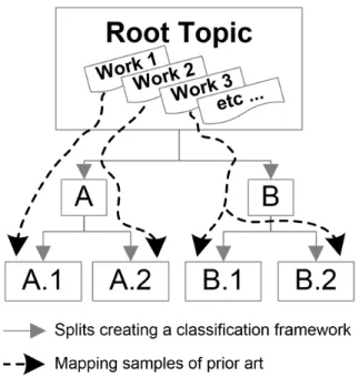
As already mentioned in the introduction to the present text (Figure 1.5), this avenue is currently being explored by active research. Apparently, it is possible to identify state-of-the-art works that can be placed under more than one leaf of the classification framework. Measurement of the flux and energy spectrum of cosmic-ray-induced neutrons on Earth.
Application of three physical fault injection techniques to the experimental evaluation of Martian architecture. In Proceedings of the Conference on Design, Automation and Test in Europe (San Jose, CA, USA, 2013), EDA Consortium, p.
![Figure 2.3: Crude timeline of indicative European projects in the vicinity of performance dependability and reliability [227]](https://thumb-eu.123doks.com/thumbv2/pdfplayerco/303122.42324/61.680.128.550.98.342/timeline-indicative-european-projects-vicinity-performance-dependability-reliability.webp)
![Figure 3.3: Flowchart of wavapprox tool: Each 𝑉 𝑔𝑠 signal is handled according to its initial format, finally providing a CDW approximation [234].](https://thumb-eu.123doks.com/thumbv2/pdfplayerco/303122.42324/72.680.216.466.103.319/figure-flowchart-wavapprox-𝑔𝑠-handled-according-providing-approximation.webp)
![Figure 3.5: Accuracy assessment of the atomistic BTI model of Equation 3.7 for various degrees of CDW-compression [234].](https://thumb-eu.123doks.com/thumbv2/pdfplayerco/303122.42324/75.680.82.604.125.826/figure-accuracy-assessment-atomistic-equation-various-degrees-compression.webp)

![Figure 3.7: Equations 3.9 and 3.10 enable full support of bias and temperature variations in the CDW-based BTI simulation framework [234].](https://thumb-eu.123doks.com/thumbv2/pdfplayerco/303122.42324/78.680.119.567.122.352/figure-equations-enable-support-temperature-variations-simulation-framework.webp)
![Figure 3.9: Destinction between “fast” and “slow” defects [234]](https://thumb-eu.123doks.com/thumbv2/pdfplayerco/303122.42324/81.680.90.591.115.480/figure-3-9-destinction-fast-slow-defects-234.webp)