Budapest University of Technology and Economics Faculty of Electrical Engineering and Informatics
Department of Electronics Technology
Dániel Straubinger
NOVEL ASPECTS OF REFLOW SOLDERING IN ELECTRONICS
MANUFACTURING
Ph.D. Dissertation
TUTOR
Dr. Attila Géczy
Table of contents
1 Introduction ... 4
1.1 Surface Mount- and Reflow Soldering Technologies ... 4
1.2 Reflow profile measurement in the electronics manufacturing industry ... 12
1.3 Reliability concerns in electronics manufacturing ... 13
1.4 Research objectives ... 16
2 Heat distribution inside PCB substrates during reflow soldering ... 19
2.1 Modelling approach ... 19
2.2 Applied materials and methods ... 22
2.3 Results and discussion ... 24
2.3.1 Validation measurement ... 24
2.3.2 Numerical results ... 24
2.4 Discussion of the results ... 31
3 Effect of geometry variations on the temperature response of thermocouples .... 32
3.1 Materials and model used for TC modelling ... 33
3.2 Details and mesh analysis of the simulation ... 39
3.3 Results ... 42
3.3.1 Validation measurements ... 42
3.3.2 Effect of different heat transfer coefficients ... 45
3.3.3 Effect of different insulation lengths (L) ... 47
3.3.4 Effect of different insulation types (I) ... 50
3.3.5 Effect of different wire types (W), insulation thicknesses (T) and hot spot radiuses (R) ... 52
3.4 Discussion of the results ... 54
4 Solder beading phenomenon of surface mounted electrolytic capacitors ... 56
4.1 Experimental ... 58
4.1.1 Identifying failure mode ... 59
4.1.2 Analysis of the reflow soldering processes... 59
4.1.3 Material analysis ... 60
4.1.4 Design aspects of the component ... 60
4.2 Results ... 61f 4.2.1 Failure analysis ... 61
4.2.2 Analysis of the reflow soldering processes... 62
4.2.3 Material analysis ... 63
4.2.4 Component design ... 64
4.3 Discussion of the results ... 69
5 Effect of high current density in chip-size passive SMD lead-free solder joints .. 71
5.1 Introduction to electromigration ... 71
5.2 Materials and methods ... 75
5.2.1 Current density in SMD solder joints ... 75
5.2.2 Experimental ... 76
5.2.3 Analysis methods ... 79
5.3 Results on FR4 substrates ... 81
5.3.1 Non-destructive analysis ... 81
5.3.2 Cross-sectioned samples ... 82
5.4 Results on ceramic-based substrates ... 83
5.4.1 Non-destructive analysis ... 83
5.4.2 Microstructure analysis on cross-sectioned samples ... 84
5.4.3 Characteristics of the intermetallic layer ... 89
5.4.4 Shear test results ... 91
5.5 Discussion of the results ... 94
6 Summary and outlook ... 97
7 Novel scientific results ... 99
7.1 Thesis points ... 99
7.2 Practical Utilisation of the Results ... 103
8 List of publications ... 105
8.1 Publications Related to Thesis Points ... 105
8.2 Additional publications ... 107
References ... 109
Acknowledgement ... 125
1 Introduction
1.1 Surface Mount- and Reflow Soldering Technologies
Surface mount technology (SMT) started to revolutionize the electronics industry in its early days in the 1960s. SMT technology uses components without the need for through holes for soldering thanks to the different soldering surfaces (pads) and leads on the components. Nowadays, the majority of the components are surface mounted devices (SMD) which enable manufacturers to utilize both sides of the printed circuit boards (PCB) by soldering the components onto soldering surfaces instead of metallized vias, meaning that the functional density of the product can be increased. Integrated circuits and passive components are also available in various forms. Component leads (such as flat gull wing, round gull wing, and J lead) are manufactured in a way that they can be soldered onto flat soldering surfaces. Modern integrated circuits (e.g. processors, memory modules) most commonly use the ball grid array (BGA) case type, where spherical solder bumps are used as terminations organized in a matrix form. Components are also available with soldering terminations instead of leads (e.g. QFN, TO-LL, MELF, passive chip components). The lead or termination of the components can have a wide range of different material compositions and surface finishes (enabling and preserving solderability). Chip-sized components are widely and commonly used in the size code 0201 (0.6 mm × 0.3 mm), 0402 (1 mm × 0.5 mm) and 0603 (1.6 mm × 0.8 mm) in mass manufacturing. The reduction in the size of the components is an ongoing process, and components with the size of 01005 (0.4 mm × 0.2 mm) and 008004 (0.25mm × 0.125 mm) are also available.
Fig. 1.1. Different SMD components
Reflow soldering in SMD technology is used in the electronics manufacturing process to create mechanical and electrical contact between the SMD components and the PCB. Since the ROHS regulations in 2006, most electronic assemblies use lead- and halogen-free solder pastes. However, high-reliability industries such as aerospace, automotive and biomedical still use leaded solders for specific applications. The solder paste contains a mixture of metal powder, flux, and rheological additives. The primary function of the flux is to remove the metal oxides from the soldering surfaces during the process, providing a reliable solder joint by allowing proper wetting. The flux and rheological additives are also crucial to achieving the desired rheological property of the solder paste. The solder particles are suspended in the flux, which protects them from oxidation. A couple of critical process steps can describe the surface mount technology:
solder paste deposition, component placement, reflow soldering, and the inspection methods for failure prevention and detection between and after the process steps, as detailed below.
The solder paste is automatically deposited onto the soldering surfaces by either dispensing or, more commonly, by stencil printing. The stencils are usually made of stainless steel or nickel. The printing machine uses, in most cases, a metal squeegee to print the paste. The width, angle, speed, and applied force should be selected accordingly for the given assembly. Apertures (tiny holes) are manufactured accordingly to the soldering surfaces in the stencil, mainly by using the electroforming manufacturing method or laser cutting. The aperture walls can be covered with nanocoating to provide even better solder paste release.
After the solder paste is deposited onto the PCB pads, the components are placed onto the solder paste with automatic pick & place machines. The machines use vacuum nozzles to pick up the components, and linear motors position the nozzle (with µm range accuracy) according to the manufacturing files, which say where the components should be placed.
To form the solder joints, the solder paste needs to be heated for the solder alloy to melt (reflow). The soldering is done accordingly to a predefined reflow soldering profile. A process window is usually defined with a minimum and maximum temperature for the soldering intervals. Fig. 1.2. illustrates a reflow profile for soldering, and the profile sections apply to solder alloys containing lead and lead-free solders.
Fig. 1.2. Reflow soldering profile with the relevant sections [1.1]
All components should fulfil being in the process windows, even though sizes, materials, and thermal properties usually have a wide spread across the assembly. As Fig. 1.2. shows, the main sections of the reflow profile are preheating, soaking, reflow and cooling. Proper slope and spent time in the zones are necessary to achieve even heating of the PCBs and to form a solder joint with a required microstructure (such as intermetallic layer thickness and grain size).
For the characterization and comparability of the reflow profile, the heating factor is widely used in the literature and the industry. The heating factor (𝑄𝜂) can be used to optimize the quality of solder joints [1.2, 1.3] and defined as Eq. 1.1 [1.4-1.6].
𝑄η= ∫ (𝑇(𝑡) − 𝑇𝑚)
𝑇2 𝑇1
𝑑𝑡 (Eq. 1.1)
Where 𝑇(𝑡) is the measured temperature on the assembly and 𝑇𝑚 is the melting point of the used solder alloy, 𝑇1 is the time when the melting point is reached during heating, 𝑇2 is the time when the solder solidifies in the cooling phase. The maximum temperature difference between measured components on the assembly is usually denoted with Δ𝑇.
To properly form a solder joint, an intermetallic layer (IML) of intermetallic compounds (IMC) should be present between the substrate and the solder. The formation of the IML is a metallurgical reaction between the molten solder and metallization on the substrate.
For a lead-free Sn-3Ag-0.5Cu (SAC305) solder alloy, the most common intermetallic compounds are Cu3Sn, Cu6Sn5 and Ag3Sn [1.7]. The IML thickness plays an essential role in solder joint reliability since an enlarged thickness could cause reduced joint strength [1.8]. The heating factor is also an often-used parameter when comparing IMC and IML formation [1.9-1.10].
The soldering itself can be performed using multiple reflow soldering methods.
The most common technologies used in mass manufacturing are forced convection soldering, vapour phase soldering (VPS) and infrared reflow soldering. There are offline and inline ovens available for the different methods. The offline methods are only used for lower quantities since it requires manual handling of the assemblies. The inline oven uses a conveyor belt to automatically transport the assemblies through the oven (Fig. 1.3.) and the manufacturing line.
Infrared (IR) reflow soldering ovens use infrared heaters and radiation heat transfer methods without the addition of forced convection. They were common in the early stages of reflow soldering. However, nowadays, forced convection reflow ovens give the majority of the industry. The infrared heat transfer can be expressed with the Stefan-Boltzmann law (Eq. 1.2).
𝑃 = 𝜖 ∙ 𝜎 ∙ 𝐴 ∙ (𝑇𝑠4− 𝑇𝑏4) (Eq. 1.2)
Where P is radiation heat transfer per unit area [W/m2], 𝜖 is the emissivity of the source, 𝜎 is the Stefan-Boltzmann constant [W/(m2K4)], A is the surface area [m2], Ts is the temperature of the heat source, Tb is the temperature of the assembly. The heating power and the speed of the conveyor belt can be used to control and optimize the reflow profile in the different zones. The main challenge in the technology was attributed to the widely
different absorption of energy due to the different colours of surfaces and reflections [1.11].
Forced convection reflow uses a matrix inlet nozzle configuration to flow the heated gas to the process zone from over and under the PCB board using fans. The perpendicular matrix nozzle inlets ensure the lowest possible turbulence in the gas flow.
Both air and nitrogen (with a limited remaining oxygen level) can be used for soldering.
Mass manufacturers use nitrogen because it produces better soldering quality due to the limited oxidation. Inside the oven are different zones with different gas temperatures (such as pre-heating, peak, and cooling, as seen in Fig. 1.3.).
Fig. 1.3. Cross-section view of a typical forced convection reflow oven, illustrating the different heating and cooling zones and the internal structure [1.12]
The heat transfer in a forced convection reflow oven can be expressed by the convection heat flow rate (Newton’s law) [1.13-1.15].
𝑄𝑐̇ (𝑡) = ℎ ∙ 𝐴 ∙ (𝑇𝑏(𝑡) − 𝑇(𝑡)) (Eq. 1.3) Where 𝑄𝑐̇ is the heat transferred per unit time, h is the heat transfer coefficient [W/(m2K)], A is the heat transfer surface, Tb is the temperature of the assembly, and T is the temperature of the gas. The heat transfer coefficient is complex and depends on the parameters of the gas and the assembly, such as gas density, angle of incidence of the gas flow, surface roughness and different components on the board [1.16]. The heat transfer coefficient of convective reflow soldering was reported to be around 60 W/(m2K) [1.17], which is used in this work also. Forced convection reflow soldering provides more uniform heating compared to IR reflow.
Vapour Phase Soldering (VPS) is a reflow soldering method based on condensation. A unique polymer fluid, Galden, is used for the process. The boiling point of the fluid determines the maximum physical temperature of the soldering process.
Fluids with different boiling points are available (such as 170 °C and 230 °C). The most basic VPS reflow ovens use heaters immersed in the Galden to boil it and create a work zone with saturated vapour. The assemblies are lowered into the vapour, where the liquid condensates onto the assembly (PCB with mounted components) and the latent heat melts (reflows) the solder paste [1.18, 1.19]. A typical structure of a VPS oven construction is illustrated in Fig. 1.4.
Fig. 1.4. Standard vapour phase soldering oven construction illustrating filmwise condensation on the PCB [R1]
By vertically moving the assembly, real-time profiling can be achieved [1.20]. There are more complex solutions and methods available for VPS soldering. The aforementioned is the basic approach. Newton’s law (Eq. 1.3) can be used to describe the heat transfer in this case also. The heat transfer coefficient depends on several factors, including properties of the Galden fluid, angle of the assembly, heating power of the heating elements, surface properties, and thickness of the condensate. Besides the advantage of the fixed boiling point and thus preventing overheating, the heating of the assembly is the most uniform in this case from all reflow methods because the condensation happens for the whole assembly simultaneously. A disadvantage of the method is that the soldering of fluid-sensitive components might not be impossible. The heat transfer coefficient of the VPS process depends on several factors but is usually reported from 90 W/(m2K) to up to several hundred [1.21-1.23]. A short, summarized comparison of the different reflow methods can be seen in Table 1.1.
Table 1.1. Comparison of different reflow methods [1.39]
Features Infrared reflow Forced convection
reflow Vapour Phase Soldering Heat transfer
principle radiation forced convection condensation
Heat transfer equation
𝑃 = 𝜖 ∙ 𝜎 ∙ 𝐴 ∙ (𝑇𝑠4− 𝑇𝑏4)
(Eq. 1.2) 𝑄𝑐̇ (𝑡) = ℎ ∙ 𝐴 ∙ (𝑇𝑏(𝑡) − 𝑇(𝑡)) (Eq. 1.3)
Advantages
Rapid heat transfer and heat recovery. Wide range
of temperatures.
Evenly heated components and assemblies due to the hot
air/nitrogen flow.
The use of nitrogen limits oxidation.
The whole assembly is heated evenly and rapidly
due to condensation.
The boiling point limits the maximum temperature.
Custom ovens can be made for massive assemblies (e.g.
aerospace industry).
Disadvantages
Heat transfer highly depends on surface features and colours;
therefore, it is a complex task to heat an assembly
evenly.
Temperature monitoring is difficult in the work
zone.
A high flow rate is required to achieve a high
heat transfer coefficient, which needs optimisation
to prevent component skewing.
For very long assemblies, even heating is a
challenge.
Heating can be too intensive for specific
components.
Soldering of moisture-sensitive components may not be
possible.
Slightly lower yield than in the case of forced
convection.
The quality of the components, assemblies, and solder joints refers to how they are conform to requirements and standards. Reliability, on the other hand refers to the ability to perform their intended functions consistently and without failure over a specified period of time. Inspection methods and quality gates are integrated into the mass manufacturing process to ensure the best possible quality and cost-effectiveness. The earlier the failure is detected, the smaller the defect cost. A typical structure and used machines in a manufacturing line are illustrated in Fig. 1.5.
Fig. 1.5. A surface mount manufacturing line with the inclusion of (automatic) inspection methods [1.24]
After the stencil printing, the solder paste deposition is analysed by an automated three-dimensional solder paste inspection (SPI) system. The deposited solder paste volume, area and height are checked against specification limits (compared to the nominal values resulting from the stencil aperture), and even contamination on the pad can be detected. The measurement values can be used for Statistical Process Control (SPC) [1.25] and closed-loop control of the solder paste printing process [1.26]. After the component placement is performed, it is possible to optically inspect the placement quality (such as position offset, missing component, and reversed polarity). During the reflow process, the surface tension can also correct the position offset and rotation [1.27].
After the reflow soldering oven, the solder joints can be investigated with automated optical inspection (AOI), automated or manual X-Ray (MXI, AXI) or in-circuit tests (ICT) to ensure the electrical properties by measuring the assemblies on specific test points. AOI analysis the wetting angle of the solder joints; can detect solder balls and solder beads if present next to the components, and also detects missing solder joints with the use of cameras. ICT can measure between measurement points included in the assembly using spring-loaded electrodes [1.28]. The measurements include measuring capacitance, inductance, and resistance values. X-Ray inspection is necessary for certain types of components when the optical inspection is insufficient because the solder joints are not visible. Many components have optically hidden leads, including BGA package, QFN, and electrolytic capacitors.
1.2 Reflow profile measurement in the electronics manufacturing industry
As detailed in the previous chapter, the reflow profile is crucial in reflow soldering technology. Knowing the temperature of the PCB, components and solder joints is required for process optimisation. Multi-channel data acquisition systems (DAQ) are used with connected thermocouples. Thermocouples use different metal alloys as wires joined at one end, usually by welding, called the hot spot or hot junction. The measurement is based on the Seebeck effect. If there is a temperature difference between the hot spot and the cold junction, the temperature difference can be measured in steady-state, according to the following equations (Eq. 1.4-1.5) [1.29].
∇𝑉 = −𝑆𝐴𝐵∇𝑇 (Eq. 1.4)
𝑆𝐴𝐵 = lim
Δ𝑇→0ΔϵAB/Δ𝑇 = 𝑑𝜖𝐴𝐵/𝑑𝑇 (Eq. 1.5)
Where the ∇𝑉 is the voltage gradient, ∇𝑇 is the temperature gradient, and SAB is the Seebeck-coefficient [𝜇𝑉/𝐾] for materials A and B, 𝜖𝐴𝐵 is the Seebeck electromotive force (EMF). For the common thermocouple types (different wire materials), the Seebeck-coefficient is characterised; thus, the DAQs can compensate for their nonlinearity [1.29]. The measured voltage difference between the cold junctions is amplified, and the temperature is calculated, which is proportional to the temperature of the hot spot.
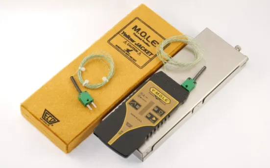
Construction can vary; however, in the electronics industry, K (Chromel-Alumel), J (Iron-Constantan) and T (Copper-Constantan) type thermocouples with a wire diameter between 100 µm to 200 µm are commonly used. The wire, in most cases, is twisted to have better immunity against electromagnetic interference and is also covered with insulation. Usually, from 3 up to 12, thermocouples can be connected to an industrial DAQ. The usage of the same DAQ for all the used thermocouples is necessary because of the cold point compensation and timely synchronization of the measurements. An example of a compact DAQ system can be seen in Fig. 1.6.
Fig. 1.6. V. M.O.L.E. reflow profiler with thermocouples and thermal insulation jacket
The acquisition devices are battery-powered and placed into a thermally insulated case to withstand the reflow soldering peak temperatures. Thermocouples are usually mounted onto solder joints, on top of heat-sensitive components (e.g. electrolytic capacitors, BGAs) or onto the PCB surface. The easiest attachment methods are using aluminium tape or Kapton tape. However, using tapes may result in a more significant measurement error [1.30]. Kapton tape is not recommended for VPS due to the condensation of the Galden [1.31, 1.32]. For better stability and thermal conductivity, SMD adhesive or soldering with a solder alloy having a high melting point (higher than the peak temperature of the reflow) is usually used. Components with different sizes and heat capacities are usually selected for reflow profile monitoring. For example, if present, the measurement of chip components, electrolytic capacitors, BGAs, large transistors and inductors is recommended since it is an important aspect to cover the most comprehensive range possible.
1.3 Reliability concerns in electronics manufacturing
Despite the strictly monitored process parameters, several failures can occur in the SMT process due to its complexity. Even if a product fulfils reflow soldering quality requirements, its reliability can be reduced in case of suboptimal process parameters or due to certain environmental effects during its lifetime. In this section, soldering issues are briefly presented, for which this dissertation aims to provide novel approaches and
solutions. These aspects are detailed in depth in the related chapters discussing the novel results. The detection and prevention of these failures are required for high-reliability industries.
During the soldering process, the PCB and the components undergo a very high-temperature change when heated to the peak temperature (~250 °C in lead-free soldering) from room temperature and cooled down in the end. This could pose a risk of thermomechanical failures. The alternation in the shape of the PCB substrate and larger flat components is referred to as warpage. The differences between the coefficient of thermal expansion (CTE) of the components and the substrate can even increase the number of soldering failures, such as open solder joints. After the assemblies are cooled down, the residual warpage can be measured [1.33]. However, its extent can be much more significant throughout the process. Therefore, the dynamic behaviour is often investigated with simulation, both for PCBs [1.34, 1.35] and for components [1.36-1.38].
Excessive intermetallic layer (IML) formation can also cause open solder joint failures [1.39]. Head in pillow refers to the phenomenon where the bump of a BGA package and the deposited solder paste is not calescence during the reflow soldering (Fig. 1.7, A)[1.40]. The failure is often caused by the warpage of the component [1.41].
Besides the material composition of the PCB and the internal construction of ICs [1.42], warpage-related problems are often associated with the reflow profile. They can be reduced or prevented by reflow profile optimisation [1.43,1.44]. The novel biodegradable PCB substrates, such as those made of polylactic acid (PLA), might need an even narrower process window for the reflow profile due to their considerably low glass transition temperature (Tg) [1.45].
A common phenomenon in the case of chip-sized components is tombstoning (Fig. 1.7, D), which refers to an open solder joint caused by unbalanced wetting forces at the component terminals [1.46]. The issue depends on the printed solder paste quality, placement offsets, preheating of the assembly, wettability and dimensions of the component metallization and solder pads [1.47]. Thermal asymmetry, causing a timely difference in the melting of solder paste at the different component terminals, might be resulting in the tombstone effect (referring to the failure in which case one terminal of the component has an open joint while the wetting force lifts the component at the other terminal; Fig. 1.7, D). The measurement of this thermal asymmetry at the solder joints requires very high accuracy.
Chip components are also affected by solder beading. Solder beading refers to the phenomenon where larger-sized solder balls are created during the reflow soldering process (Fig. 1.7, C). The solder beads, in most cases, can be found at the side of the components. The solder beads might be acceptable based on their diameter. They pose a reliability risk because, if displaced, they may short-circuit small raster components in the assembly. Using home plate and inverse home plate apertures for stencil printing was reported to reduce their occurrence [1.48,1.49] effectively.
The previously mentioned ongoing reduction in SMD component sizes is always challenging for the industry. Smaller components require smaller stencil apertures and, therefore, small solder paste particles [1.50,1.51] and, of course, higher placement accuracy. In addition, the reduced sizes can also introduce reliability problems, such as electromigration. The current density is also increased in the solder joints due to the smaller components, thus smaller solder joint sizes. High current density can induce electromigration in the solder joint. Electromigration describes the atomic motion in a metal under the influence of an applied electric field [1.52]. It was widely investigated for silicon technology [1.53, 1.54], in SMD technology, mainly in the case of BGA and flip-chips solder joints. The material transport in severe cases can cause open interconnections or short circuits. An example is illustrated for the case of CVD Cu lines stressed at 238 °C and 8 MA/cm2 (Fig. 1.7, B). The effect, however, depends largely on the material composition and microstructure.
Fig. 1.7. Failure modes and alterations in electronics manufacturing. A: head-in-pillow of BGA component [1.55], B: electromigration induced void and hillock formation in copper interconnect [1.56],
C: mid-chip solder balling [1.57], D: tombstoning of SMD component [1.58]
1.4 Research objectives
The reliability of electronic assemblies is crucial in several fields, including the automotive-, air- and aerospace industries. The most demanding applications require an optimised process, including the reflow profile, to prevent soldering failures. In my work, I aim to provide an improved understanding and description of the reflow soldering process and reliability.
Electronics manufacturing and standardisation have established strict guidelines in reflow soldering. The products must fulfil a specific reflow profile. Researchers investigate the optimised reflow profile using finite element simulation (FEM) and machine learning, which in most cases requires a lot of computational power and is thus time-consuming. Manufacturers often use DAQs and thermocouples to measure the temperature profile of a particular assembly, but covering all solder joints is impossible.
In several industries, product change (including manufacturing for different customers or rolling out a new generation) is very frequent, and every product and profile is slightly different. I approached this topic by trying to find the limits of the applicability of heat transfer coefficient based explicit modelling, which would be able to provide on-the-fly
profile predictions. It is also not covered thoroughly in the literature how the temperature uniformity of the PCB affects warpage. The method can improve the soldering quality and be used in agile environments in the Industry 4.0 mindset.
Validation measurements are required to validate models and simulations and even reflow profiles. The electronics industry uses thermocouples daily. The effect of specific parameters of the thermocouple, including the attachment methods, was previously investigated. However, the literature has shortcomings regarding some parameters of the thermocouples, including the effect of small changes in geometry, such as the uninsulated wire length around the hot-spot. In the application of thermocouples in the electronics industry, in several use cases, sub-second differences could have importance (such as the measurement of the two terminals of a tombstoning component).
I aim to reveal the effect of those changes, making it possible to select the measurement tool providing sufficient accuracy for the measurements.
A circuit with high reliability should fulfil IPC guidelines (electronics standards used by the electronics industry) and be free of soldering defects. Solder beading could cause fatal failures in case of making a short circuit. The literature covers the case of chip- size components, where the solder ball or solder bead is optically detectable. On the other hand, several components have a construction, making it impossible to inspect optically whether a solder bead occurs during the reflow process. One example is electrolytic capacitors (a frequently used component), which can only be analysed with an X-Ray, which is not cost-effective. Electronics assemblies have such a high integration level that a standard electrolytic capacitor can cover several vias or PCB traces under itself, where the solder bead is a potential risk. I aimed to provide an understanding of the solder beading phenomenon under such components, reveal the effects of the design and propose a preventive solution.
Due to the decreasing SMD component sizes and increasing current densities, it is essential to investigate the possible failure modes attributed to electromigration.
Electromigration studies are unavailable for chip-sized components. However, the currently available SMD component sizes could also result in critical current densities;
therefore, their reliability must be ensured at the design level [1.59]. Because of the reasons mentioned above, further research in the field is necessary to assess the potential risk.
The research on the literature revealed the relevance of the aforementioned topics and the resulting questions. I have set the following points as milestones of my research:
• To investigate the temperature distribution inside different PCB substrates (including classical FR4, ceramics and biodegradables) during the reflow solder process to obtain the limitation of the applicability of heat transfer coefficient based explicit modelling, which could be used as an efficient method for reflow profile prediction in the Industry 4.0 mindset.
• To investigate the effect of measurement systems on the data describing the reflow soldering process, focusing on the construction of thermocouples and the effect of the construction changes for optimised measurement accuracy.
• To investigate the solder beading phenomenon in the case of SMD electrolytic capacitors, discover reliability concerns, and determine and optimise the soldering process and components design to eliminate the issue.
• To investigate the electromigration phenomenon in small-sized, passive SMD components lead-free solder joints, discovering potential reliability concerns regarding the ever-increasing power and current density in SMD packaging.
2 Heat distribution inside PCB substrates during reflow soldering
The soldering reliability and thermomechanical aspects of the assemblies are directly affected by the heat transient behaviour in the PCB substrates and components.
Previously, heat transfer coefficient based explicit modelling was used on horizontally aligned substrates[2.1]. Modelling the thermal behaviour of electronics assemblies is considered the primary approach to improve the soldering profile and is also cost- effective. Modelling can reveal aspects in the process that are hard to identify using measurement devices [2.2, 2.3]. Novel measurement approaches are also introduced to characterize reflow processes, but those methods are mainly focusing on the identification of the soldering work zone [2.4, 2.5]. It is necessary to investigate the limitation in the application of explicit modelling. In my work, I have focused on presenting an analytical solution of the resulting temperature distribution within different types of PCB substrates.
Different reflow processes are represented in this approach with their characteristic heat transfer coefficients. The temperature distribution is calculated analytically based on the one-dimensional transient heat conduction theory. The results can be used to determine for different types of substrate materials and thicknesses whether the explicit modelling can be used to describe the heating of an assembly. The aim is to analyse the possibility of explicit thermal modelling of a complete circuit board assembly. Due to the low computational power requirement of the explicit modelling, adaptive reflow profile control could be implemented in a manufacturing environment by adjusting the varying parameters for the different products, which is in line with the fully automated, connected and closed-loop system of the Industry 4.0 directives.
2.1 Modelling approach
The heat transient behaviour of a printed circuit board (considering bare substrates without the much thinner copper layer as a simplification) can be considered as a plane wall geometry because the thickness is at least one magnitude smaller than the lateral dimension of the substrate. Modelling of PCB substrates, therefore, can be considered as plane wall geometries, aligned horizontally, for all reflow methods.
Fig. 2.1. shows the modelling aspects, where the PCB assembly is considered a horizontal plane wall geometry. The reflow soldering process is described with a constant heat transfer coefficient, which is assumed for both surfaces (top and bottom side).
Fig. 2.1. right shows the cross-section of the PCB where L is the half thickness [m], and the midplane or central point inside the PCB is where x = 0. The investigated geometry is symmetrical to the midplane. Therefore, the aforementioned constant heat transfer coefficient can be assumed to be the same on both sides (where -L < x < 0 and 0 < x < L).
Fig. 2.1. Heat transfer on SMD assembly with highlighted horizontal plane wall geometry (cross-section of a PCB) [L1]
Using the symmetry, the problem can be defined for only half of the geometry (i.e. 0 ≤ x ≤ L), and the results are also applied to the other half (i.e., L ≤ x ≤ 0). The one- dimensional heat transient problem can be expressed by the following equations [2.6]:
𝜕2𝑇
𝜕𝑥2 = 1 𝛼
𝜕𝑇
𝜕𝑡 (Eq. 2.1)
𝛼 = 𝑘 𝜌𝑐𝑝
(Eq. 2.2)
where x [m] represents the vertical position inside the PCB (for 0 ≤ x ≤ L), α is the thermal diffusivity of the material [m2/s], k [W/(mK)] is the thermal conductivity, ρ [kg/m3] is the density, and cp [J/(kgK)] is the specific heat capacity. The boundary conditions are the following: constant heat transfer coefficient, constant material properties and uniform initial temperature. The initial state is described with the boundary conditions according to the following equations:
𝜕𝑇(0, 𝑡)
𝜕𝑥 = 0 𝑎𝑛𝑑 − 𝑘𝜕𝑇(𝐿, 𝑡)
𝜕𝑥 = ℎ[𝑇(𝐿, 𝑡) − 𝑇∞] (Eq. 2.3)
𝑇(𝑥, 0) = 𝑇𝑖 (Eq. 2.4) The differential equation can be written in a dimensionless form, with the definition of a dimensionless space variable (Eq. 2.5) and a dimensionless temperature variable (Eq. 2.6) as follows:
𝑋 =𝑥 𝐿
(Eq. 2.5)
𝜃(𝑥, 𝑡) =𝑇(𝑥, 𝑡) − 𝑇∞ 𝑇𝑖 − 𝑇∞
(Eq. 2.6)
The dimensionless solution for the plane wall geometry with 2L thickness can be expressed as follows (Eq. 2.7):
𝜃 = ∑ 4𝑠𝑖𝑛𝜆𝑛
2𝜆𝑛+ sin (2𝜆𝑛)𝑒−𝜆𝑛2𝜏cos (𝜆𝑛𝑥 𝐿 )
∞
𝑛=1
(Eq. 2.7)
where 𝜆𝑛’s are the roots of Eq. 2.8 and Bi (Eq. 2.9) is the dimensionless heat transfer coefficient (Biot number), and L is the characteristic length of a given geometry [m], which is the half thickness of the PCB in our case.
𝜆𝑛𝑡𝑎𝑛𝜆𝑛 = 𝐵𝑖 (Eq. 2.8)
𝐵𝑖 =ℎ𝐿 𝑘
(Eq. 2.9) The one-term approximation of the dimensionless temperature in the horizontal plane wall problem can be calculated with Eq. 2.10 and Eq. 2.11:
𝜃𝑤𝑎𝑙𝑙 =𝑇(𝑥, 𝑡) − 𝑇∞
𝑇𝑖 − 𝑇∞ = 𝐴1𝑒−𝜆12𝜏 cos(
𝜆1𝑥
𝐿 ), 𝜏 > 0.2 (Eq. 2.10)
𝜏 =𝛼𝑡
𝐿2 = 𝐹𝑜 (Eq. 2.11)
where 𝜏 is the dimensionless time (Fourier number) and λ1 is the first root between 0 and 𝜋 of Eq. 2.8. A1 is obtained by Eq. 2.12:
𝐴1 = 4sin (𝜆1) 2𝜆1 + sin (2 𝜆1)
(Eq. 2.12) When τ is meeting the <0.2 criterion (Eq. 2.10), the approximation results in error only under 2% [2.6].
2.2 Applied materials and methods
In my work, I aim to cover a wide range of material types and PCB thicknesses used in the industry. The investigation covers the most common, glass fibre reinforced epoxy substrates (FR4), polyimide polymer, which is used for flexible electronics [2.7], typical ceramic-based circuits used in high frequency and power electronics applications [2.8] and novel biodegradable substrates, which at a certain point could lead the industry towards greener electronics such as polylactic acid (PLA) and cellulose acetate (CA). The applicability of biodegradable substrates due to thermomechanical properties are subject of active research [2.9-2.11]. The thickness of the substrates is investigated from 0.25 mm up to 2 mm with a 0.25 mm step size. The work focuses on the thermal behaviour of the bare substrates; outer and internal copper layers are not considered. The copper layer thickness is usually at least one magnitude smaller than the substrate thickness, and the substrate coverage is not uniform. Also, it is not uncommon in consumer electronics that a product is built onto a one-sided single-layer PCB which is very similar to the investigated bulk case. The inclusion of irregular copper trace patterns would interfere with the generalised findings; however, their inclusion might be introduced in later research.
The PCB board materials and their used properties are detailed in Table 2.1.
below.
Table 2.1. PCB material properties [2.12, 2.13]
Material Density [kg/m3]
Thermal conductivity
[W/(mK)]
Specific heat capacity [J/(kgK)]
Thermal diffusivity [m2/s]
Al2O3 3900 25 880 7.28E-06
BeO 2850 248 1005 8.66E-05
Polyimide 1340 0,604 1010 4.46E-07
PLA 1240 0,13 1800 5.82E-08
CA 1270 0,25 1470 1.34E-07
FR4 1900 0,29 600 2.54E-07
Although amorphous polymers undergo measurable thermal parameter change (for example, in thermal diffusivity [2.14]) around the glass transition temperature (Tg), their effect is often neglected in the modelling of assembly or oven-level reflow soldering, even in recent papers [1.23, 2.15-2.17], and also for the analysis of thermomechanical behaviour [1.35, 2.18]. The thermal properties and the stress inside the substrates are also
influenced by their exact composition and manufacturing process, according to Lee [1.39]; therefore, single describing thermal property values are unavailable.
The investigation considered forced convection reflow soldering and VPS, with 60 W/(m2K) [1.17, 1.25] and 210 W/(m2K) heat transfer coefficients, respectively, heating the PCB from both sides. These parameters could vary for different soldering oven constructions and settings. However, the work aimed to differentiate the two methods without analysing the heat transfer coefficients in further depth (such as how they depend on the process). In the results section, to compare the different reflow methods and substrate materials, the temperature difference (ΔT) between the surface and the midplane of the substrates and the time to reach the melting point of the solder alloy is used. It is assumed, based on their definitions, that the time required to reach a given temperature (e.g. a melting point of a solder alloy) on the surface primarily depends on the volumetric heat capacity of the material, while the 𝛥𝑇 mostly depends on the thermal diffusivity of the material.
As boundary conditions, the initial temperature was set to 𝑇𝑖 = 25 °𝐶 (room temperature), and the steady state temperature was set according to the boiling point of Galden HT170 type, which is 𝑇∞= 170 °𝐶. This is considered a low peak temperature in reflow soldering technology; however, certain low melting point alloys, such as Sn58Bi (with a melting point of 138°C), could be soldered, which is a popular choice of alloy for the investigated biodegradable substrates. However, the same method can be applied to different peak temperatures also.
Calculating the temperature distribution in the investigated cases was performed with the following steps. The Biot number needs to be calculated based on Eq. 2.9 and the material properties from Table 2.1. After that, 𝜆1is determined with the Generalised Reduced Gradient (GRG) nonlinear solving method by solving Eq 2.8. Then, with 𝜆1, it is possible to solve Eq. 2.10 and Eq. 2.12 explicitly.
The results were validated for a bare FR4 laminate, having the dimension of 100 × 100 × 1.5 mm (length × width × thickness). The measurement was performed in an experimental VPS oven. The soldering medium was Galden HT170 [2.19], and the temperature profiling was performed with a K-type thermocouple (having ±1 °C accuracy) attached in the board's central point. A V-Mole soldering profile DAQ was used with a 1 s sampling rate. The measurement setup consisted of commonly used
elements of a manufacturing environment. The midpoint was used to reduce the corner/edge effect of the condensation of the board; however, it is, in any case, limited to around 20 % [2.19]; thus, most of the board can be assumed to be heated evenly.
2.3 Results and discussion
2.3.1 Validation measurement
The results of the validation measurements are represented in Fig. 2.2.
Fig. 2.2. Validation measurements [L1]
At the very first stage, there is a difference between the measurement results and calculation, which can be attributed to the fact that in the case of VPS, there is intensive heating as the condensation starts in the immersion process. Bozsóki et al. revealed that the heat transfer coefficient depends on the surface temperature history. At the beginning of the process, the heat transfer coefficient is high, resulting in faster heating, and its value is reduced during the process [2.20]. The used average representative heat transfer coefficient (for simplicity and generalisation) does not represent this behaviour, causing deviation at the beginning of the simulation and measurements. However, after the first seconds, the results show a good agreement, and the differences are considered acceptable for modelling purposes.
2.3.2 Numerical results
In this section, the most representative modelling cases are discussed, according to Table 2.2. These results include different substrate thicknesses, materials with
0 20 40 60 80 100 120 140 160 180 200
0 5 10 15 20 25
Temperature,°C
Time, s
Calculated, °C Measured, °C
significantly different thermal properties (PLA and BeO), and also different reflow method types.
Table 2.2. The illustrated modelling cases [L1]
Cases Material Thickness [mm] Reflow method Changes along cases
Fig. 2.3 PLA 0.25 VPS -
Fig. 2.4 PLA 2 VPS Thickness increase
Fig. 2.5 PLA 2 Convection Reflow method
Fig. 2.6 BeO 2 VPS Material, Reflow method
The results of the test cases in Table 2.2. are represented in Figures from 2.3. to 2.6, where the temperature distribution along the substrate thickness is illustrated. In Figure 2.3. the case of PLA (having the lowest thermal diffusivity of the materials) is illustrated with the smallest thickness (0.25 mm).
Fig. 2.3. Temperature distribution over time along board thickness; 0 = centre of board (VPS; PLA, 0.25mm) [L1]
The results show that the temperature differences inside the 0.25 mm thick PLA board are practically negligible from the midplane to the surface. Figure 2.4. represents the maximum thickness with the same PLA substrate material.
Fig. 2.4. Temperature distribution over time along board thickness; 0 = centre of the board (VPS; PLA 2 mm) [L1]
Contrary to the 0.25 mm thick board, the results show significant differences for the 2 mm case. While the thin board (Fig. 2.3.) reaches approximately the maximum temperature after about 6-8 seconds, the 2 mm thick substrate (Fig. 2.4.) does not reach the maximum process temperature, not even on the surface of the substrate.
Fig. 2.5 shows the case of the forced convection reflow method, which has a moderate heat transfer coefficient compared to the VPS method.
Fig. 2.5. Temperature distribution over time along board thickness; 0 = centre of the board (Convection;
PLA, 2 mm) [L1]
The calculated results are similar to the ones observed in the case of Fig. 2.4.
However, the reached temperatures are significantly lower at the same time stamps. An approximately 50 °C temperature difference is observable between the surface and the midplane after 26 s elapsed.
Fig. 2.6. Temperature distribution over time along board thickness; 0 = centre of the board (VPS, BeO 2 mm) [L1]
Fig. 2.6. shows the results for the BeO substrate case with a 2 mm thickness. BeO has a high thermal diffusivity. It can be concluded that the temperature is practically evenly distributed inside the PCB. On the other hand, the maximum temperature for the surface is not reached within the investigated time frame. After 26 s of the process, the middle point in the PLA substrate is approximately 10 °C behind the BeO board.
Fig. 2.7. and Fig. 2.8. represents temperature differences in some selected examples. For the illustration, the more intensive VPS reflow process was used. The Tsurface-Tmidplane (ΔT) is illustrated for substrate thicknesses from 0.25 mm up to 2 mm.
Fig. 2.7. ΔT during the modelled VPS process for different PLA substrate thicknesses [L1]
Fig. 2.8. ΔT during the modelled VPS process for different BeO thicknesses [L1]
The trend of the results is the same; however, the resulting ΔT value is highly different from the significant change in thermal diffusivity of the materials.
Table 2.3 summarises the test cases presented in Fig. 2.9. and Fig. 2.10, where the modelling results for substrate thickness versus time to reach melting time and the substrate thickness versus ΔT are presented.
0 10 20 30 40 50 60 70 80 90
0 5 10 15 20 25 30
Time, s
0.25 mm 0.5 mm 0.75 mm 1 mm 1.25 mm 1.5 mm 1.75 mm 2 mm
ΔT, °C
0 0,01 0,02 0,03 0,04 0,05 0,06 0,07
0 5 10 15 20 25 30
Time, s
0.25 mm 0.5 mm 0.75 mm 1 mm 1.25 mm 1.5 mm 1.75 mm 2 mm
ΔT, °C
Table 2.3. Temperature distribution cases [L1]
Cases Reflow Method Approach Materials
Fig. 2.9, left Convection Time to reach melting temp. Full Set Fig. 2.9, right Convection ΔT at the melting point Full Set Fig. 2.10, left VPS Time to reach melting temp. Full Set Fig. 2.10, right VPS ΔT at the melting point Full Set
Fig 2.9. Convection reflow; left: Time to reach melting point on the surface with convection-based reflow for different substrates; right: ΔT at melting point with convection based reflow for different substrates
[L1]
By comparing Fig. 2.9. left, and Fig. 2.10. left, it can be seen that due to the lower heat transfer coefficient of the reflow method (lower heating intensity), it takes more time to reach the melting point of the solder. It is also shown that the surface of the technical ceramics takes the longest time to heat up, which is attributed to their larger thermal diffusivity, which enables heat to be transferred to the inside of the substrate material.
Results show that FR4 reaches the melting point the fastest, while Al2O3 is the slowest in that matter. This is attributed to the volumetric heat capacity of the materials (which is generalised with the product of their density and specific heat capacity). The resulting order of the different materials is the same for both heat transfer methods.
0 10 20 30 40 50 60 70 80 90
0 0.5 1 1.5 2
Time to reach melting point, s
PCB substrate thickness, mm
0 5 10 15 20 25 30
0.0 0.5 1.0 1.5 2.0
∆T, °C
PCB substrate thickness, mm
FR4
Polyimide
CA
PLA
BeO
Al2O3 98%
Fig 2.10. Vapour phase reflow; left: Time to reach the melting point on the surface with VPS reflow for different substrates; right: ΔT at the melting point with VPS based reflow for different substrates [L1]
Timely differences are getting significant above 0.5 mm thickness for convection and 1.5 mm for VPS, but practically negligible for thinner PCBs. Fig. 2.9. right and Fig. 2.10. right shows the temperature difference (ΔT) between the surface and the midplane of the substrates when the melting point (138 °C) is reached on the surface. The more intensive VPS process results in higher ΔT. For the ceramics (Al2O3, BeO), the ΔT is negligible. It is in line with their great thermal diffusivity and conductivity.
The order of 10 °C temperature difference along the thickness within the PCB does not have a significant effect on the soldering quality (such as by extensive thermal diffusion into the substrate). According to the literature, in the range of reflow soldering temperatures (up to 170 °C or 230 °C in certain cases), the resulting 10-15 °C temperature difference can be considered acceptable [2.21, 2.22], and therefore, the heat transfer coefficient based explicit modelling is possible with adequate error [2.1]. However, the maximum temperature difference for the polylactic acid substrate is around 20 % (relative to the soldering temperature range), while this difference is below 10 % for the other materials.
Consequently, it can be concluded that explicit modelling of the thermal behaviour of PCB substrates made of PLA material is not suggested over 1 mm thicknesses. Proneness to thermomechanical stress is the most considerable in the case of PLA substrate in accordance with Fig. 2.9. right and Fig. 2.10. right. It is supposed that in the case of equal heating from both sides, the likelihood of warpage-based failures is
0 10 20 30 40 50 60 70 80 90
0 0.5 1 1.5 2
Time to reach melting point, s
PCB substrate thickness [mm]
0 5 10 15 20 25 30
0 0.5 1 1.5 2
∆T, °C
PCB substrate thickness [mm]
FR4
Polyimide
CA
PLA
BeO
Al2O3 98%
minimal [2.23]. Nevertheless, in the case of uneven heating from the top and bottom side of PCB, PLA is going to be the most sensitive to suchlike an effect in comparison with the other analysed materials. The sensitivity of the materials is as follows: CA, FR4, polyimide and technical ceramics. From a thermomechanical viewpoint, the beginning of the soldering process may be more substantial due to the more considerable temperature differences (i.e. around 70 °C initially in Fig. 2.4.), but more severe thermomechanical behaviour is tied to an increased temperature above the glass transition temperature.
2.4 Discussion of the results
The analytical solution of the temperature difference resulting during reflow soldering was calculated based on the one-dimensional heat transient conduction theory for multiple PCB materials and thicknesses for different reflow methods (VPS and forced convection). Since the PCBs are more than one magnitude thinner than their length and with, they were considered as a plane wall geometry (common in the modelling of PCBs in reflow technology). The work covered novel biodegradable substrates next to the commonly used materials, and the thermal performance of such assemblies was assessed.
It was shown that, according to the assumptions, 𝛥𝑇 mostly depends on the thermal diffusivity of the material. In contrast, the time required to reach the melting point of Sn58Bi solder alloy on the surface primarily depends on the volumetric heat capacity of the substrate material.
Results show that temperature differences vertically inside a PCB are most probably minor from the aspect of the thermal diffusion effect throughout the melting of the solder. The maximum difference was about 10-15 °C at that point, which does not pose a significant risk to soldering reliability. On the other hand, this risk is elevated for the PLA material, in which case ΔT is greater, approximately 25-30 °C above the 1 mm thickness of the substrate. In addition, the temperature differences may not be insignificant if CTE mismatch-originated failures are analysed along the substrate thickness. PLA is the most prone to this effect, followed by CA, FR4, polyimide and technical ceramics, respectively.
3 Effect of geometry variations on the temperature response of thermocouples
This chapter presents the modelling results of different thermocouple construction and their effects on the response of the thermocouples (TC). As discussed in the introduction, thermocouples are widely used in electronics manufacturing to monitor temperature during reflow soldering [3.1]. The wire types (such as K, J, and T), insulation types and physical dimensions of the TCs have a large variety to adapt to different reflow conditions (such as the construction of the oven and the temperature range of operation).
The sensor construction, however, can alter the response of the thermocouples [3.2].
Several recent papers discuss the use cases of TCs in electronics manufacturing. They were used in investigations such as analysing the thermal conductivity of macro-sized solder joints with void content [3.3] and particular aspects of demanding LED assemblies [3.4]. They are also used for the improvement of real-time reflow profiling [1.20], as parts of a control system for reflow ovens [1.18], for measuring heat level based VPS [3.5] and for validating the reflow profile of IR reflow ovens [3.6]. Drilling processes can be monitored with TCs [3.7], as well as bonding in power electronics [3.8]. Hai and Zhu used thermocouples for the validation measurement of components reflow soldering simulation [3.9].
It was previously shown that gauge type and different attachment methods could also be crucial aspects since they influence the measurement of surface temperature [3.1].
The usage of smaller-sized thermocouples with lower heat conductivity was recommended by Shaukatullah [3.1].
Thermocouples come in a wide variety, including hot spot size, the used alloy for the wires, insulation material and design and so on. Although insulation materials might range from glass fibre and polytetrafluoroethylene (PTFE) to perfluoroalkoxy (PFA), the literature only discusses the effect of the materials and construction on the measurement during reflow soldering on a few occasions.
Alaya et. al. showed that the wire and the bulk of thermocouples affect the VPS process by altering the relation between the heat transfer medium and the assembly [3.10].
The vapour can be drawn away by the bulk of wiring in the work zone. Certain errors initiated by internal thermal conduction can be important [3.11]. The wire of the TC
around the hot spot is exposed (uninsulated), which is also heated during the reflow process. This aspect of the construction is not detailed on the datasheet but may influence the temperature of the hot spot [3.12] by increasing its temperature [3.13], but still, there are no certain conclusions drawn from this geometry aspect. The modelling of the complete connection volume with the TC with the inclusion of attachment material, groove and TC was investigated by Borovkova [3.14]. Romero et al. also modelled embedded thermocouples and their response focusing on different boundary conditions with varied parameters [3.15]. Numerical modelling of sheathed N-type TCs was presented by Chakraborty and Kadoli [3.16], where they focused on the aspects of heat transfer, not on the construction of the TC itself. The recovery factor of the thermocouple probe was evaluated from the aspect of freestream turbulence during high-speed flow [3.17]. Frankel et al. realised an analytical model of the thermocouple impulse response function based on an investigation of the transient impulse response of the thermocouple construction [3.18]. Steady-state errors of shielded TCs were investigated by computational fluid dynamics (CFD) modelling [3.19]. CFD was utilized successfully in the investigation of T-type thermocouples in a nitrogen atmosphere [3.20]. Segall suggested the application of correction curves in the TC characteristics in case of a parameter change, and to achieve that, the contact resistance, stray heat transfer of TCs and junction displacement were investigated [3.21].
Based on the literature study, I decided to focus on the construction of exposed, welded hot spot TCs and how their constructional parameter variation affects the temperature of the hot spot. The modelling of such parameters can be used in validation measurements of models, optimized process monitoring and consequently improved product quality and reliability. The presented results could also be used in improved work zone characterisation [3.22].
3.1 Materials and model used for TC modelling
The set of materials and the range of thermocouples which are investigated in our modelling are described in this section. The analysis included the following steps:
definition of the model, specification of simulation parameters, validation of the model by measurements and discussion of the simulation results and measurements.
The material properties used for the simulation are illustrated in Table 3.1. The parameters include the metals and alloys used as wires, according to the American Society
for Testing and Materials (ASTM) classified K, T and J type sensors, and the insulation materials. The type of TCs was selected accordingly to the literature study.
Table 3.1. Properties for applied materials [3.23]
Material
Material properties Thermal
conductivity [W/(mK)]
Density [kg/m3]
Specific heat capacity [J/(kgK)]
Chromel (K type) 19.2 8730 448
Alumel (K type) 29.7 8610 523
Copper (T type) 391 8940 385
Constantan (T type, J
type) 21.8 8860 393
Iron (J type) 73.9 7860 473
PFA 0.23 2150 1030
Glassfibre 1.25 2500 836
PVC 0.157 1390 1005
PTFE 0.292 2170 1500
Different thermocouple constructions were derived for the investigation as test cases summarised in Table 3.2.
![Fig. 1.5. A surface mount manufacturing line with the inclusion of (automatic) inspection methods [1.24]](https://thumb-eu.123doks.com/thumbv2/9dokorg/2497757.294340/11.893.146.793.122.405/fig-surface-mount-manufacturing-inclusion-automatic-inspection-methods.webp)
![Fig. 1.7. Failure modes and alterations in electronics manufacturing. A: head-in-pillow of BGA component [1.55], B: electromigration induced void and hillock formation in copper interconnect [1.56],](https://thumb-eu.123doks.com/thumbv2/9dokorg/2497757.294340/16.893.191.744.104.503/failure-alterations-electronics-manufacturing-component-electromigration-formation-interconnect.webp)
![Fig. 2.4. Temperature distribution over time along board thickness; 0 = centre of the board (VPS; PLA 2 mm) [L1]](https://thumb-eu.123doks.com/thumbv2/9dokorg/2497757.294340/26.893.240.698.107.420/fig-temperature-distribution-time-board-thickness-centre-board.webp)
![Fig. 2.6. Temperature distribution over time along board thickness; 0 = centre of the board (VPS, BeO 2 mm) [L1]](https://thumb-eu.123doks.com/thumbv2/9dokorg/2497757.294340/27.893.241.700.249.582/fig-temperature-distribution-time-board-thickness-centre-board.webp)
![Fig. 2.7. ΔT during the modelled VPS process for different PLA substrate thicknesses [L1]](https://thumb-eu.123doks.com/thumbv2/9dokorg/2497757.294340/28.893.281.656.111.416/fig-δt-modelled-vps-process-different-substrate-thicknesses.webp)
![Fig. 2.8. ΔT during the modelled VPS process for different BeO thicknesses [L1]](https://thumb-eu.123doks.com/thumbv2/9dokorg/2497757.294340/28.893.281.655.501.800/fig-δt-modelled-vps-process-different-beo-thicknesses.webp)
![Fig. 3.1. K-type thermocouple dimension measurement (top) and its representative CAD model (bottom) [L2]](https://thumb-eu.123doks.com/thumbv2/9dokorg/2497757.294340/38.893.249.688.103.703/fig-type-thermocouple-dimension-measurement-representative-cad-model.webp)
![Fig. 3.2. Results for τ (A) and time to reach 138 °C (B) for different mesh resolutions [L2]](https://thumb-eu.123doks.com/thumbv2/9dokorg/2497757.294340/41.893.212.727.118.309/fig-results-τ-time-reach-different-mesh-resolutions.webp)
![Fig. 3.4. Construction of the vapour phase soldering environment used for the validation measurement [L2]](https://thumb-eu.123doks.com/thumbv2/9dokorg/2497757.294340/42.893.189.751.520.753/fig-construction-vapour-phase-soldering-environment-validation-measurement.webp)
