Theory of electrical characteristics for metaloxideinsulator Schottky barrier and metal
insulatormetal structures
H. M. Gupta and Marta B. Morais
Citation: Journal of Applied Physics 68, 176 (1990); doi: 10.1063/1.347111
View online: http://dx.doi.org/10.1063/1.347111
Theory of electrical characteristics for metal ... oxlde-insulator Schottky
barrier and
ュ・エ。ャセゥョウオゥ。エッイ@... metal structures
H. M. Gupta
Departamento de Flsica IGCE, UN ESP. C. P. 178, 13500 Rio Claro SF, Brazil
Marta R Morais
Departamento de Cifmcias, Faculdade de Engennaria, UNESP, 15378 [Iha Solteira SP, Brazil
(Received 14 August 1989; accepted for publication 13 February 1990)
The metal-insulator or metal-amorphous semiconductor blocking contact is still not well understood. Here, the intimate metal-insulator and metal-oxide-insu!ator contact are discussed. Further, the steady-state characteristics of metal-ox ide-insulator-metal structures are also discussed. Oxide is an insulator with wider energy band gap (about 50
A
thick). A uniform energetic distribution of impurities is considered in addition to impurities at a single energy level inside the surface charge region at the oxide-insulator interface. Analytical expressions are presented for electrical potential, field, thickness of the depletion region, capacitance, and charge accumulated in the surface charge region. The electricalcharacteristics are compared with reference to relative densities of two types of impurities. In I
is proportional to the square root of applied potential if energetically distributed impurities are relatively important. However. distribution of the electrical potential is quite complicated. In general energetically distributed impurities can considerably change the electrical
characteristics of these structures.
I. INTRODUCTiON
The metal-semiconductor (MS) interface has played an important role in many technological developments. i-3 However, a fun understanding of the physics behind the ori-gin and electrical properties of the Schottky barriers is not yet properly understood from a theoretical point of view in spite of many works,4-l! even for crystalline materials. The metal-insulator contact, particularly that of amorphous ma-terial, is an even more complicated problem because of the uncertainty of the nature and distribution of impurities at contact. Recently many authors9
-12 have discussed the
met-al-amorphous-silicon contact because of its technological importance.
Electrical conduction through metal-insulator-metal (MIM) structures has been the subject of intensive theoreti-cal and experimental investigation in the last three dec-ades.13-14 In very thin insulating films (
<
50A),
tunneling from metal to metal is a predominant charge conduction mechanism. 15 In cases of thick films (>
1 )lm), bulk proper-ties of insulators are definitely more important. The charge conduction mechanisms in blocking contact MIM struc-tures with intermediate insulator thicknesses (1000A
to1
j.Lm) are still uncertain, while this range of insulator thick-ness is technologically the most important.
A large number of c1assicall6-17 and quantum 18 me-chanical models have been proposed for Schottky barriers. The most classical is the one proposed by Schottky in 1939, which is based on a perfect contact between the metal and semiconductor leadi.ng to Fermi-level alignment and band bending to neutralize the charge transfer. In this model, do-nor-type impurities at a single energy level are considered.4 The localized impurities are distributed throughout an amorphous material. 13 The importance of surface states and energetically distributed impurities at interface in MIS or MS Schottky barriers are well recognized.7 However, most
of the recent work is on either formation of the Schottky barrier and relation of barrier height to these impurity distri-butions, 6-19 or on the determination of energetic distribution ofthese impurities in amorphous materials,9-1O particularly amorphous silicon through the capacitance-voltage relation-ship. Mostly numerical calculations are done to obtain ener-gy di.stribution of these impurities. Tarasenwlcz and Sa-lama20 discussed the theory of the surface depletion region for a semiconductor with linearly graded impurities at a sin-gle energy level, which is important for ion-implanted de-vices.
The importance of energetically distributed impurities on variations of electrical field and potential within the de-pletion region and on electrical characteristics ofmetal-insu-lator-metal structures with blocking contacts is not dis-cussed in detail; particularly, no analytical approach is made. For detailed discussion of steady and nonsteady-state electrical characteristics of MIM structures, impurities at a single energy level are usually considered.4,21-z3 In the pres-ent paper we discuss the effects of energetically distributed impurities on electrical characteristics of Schottky barriers and MIM structures. We found that impurities can consider-ably change the electrical characteristics of these structures.
II. metaャセsemiconductor@ CONTACT
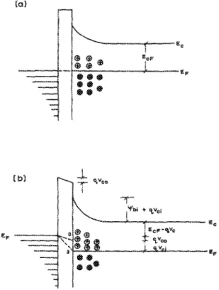
Schottky4.!6 considered a uniform positive charge den-sity in the depletion region and intimate metal-semiconduc-tor contact. When the external contact potential ( Vc ) equals zero, the general shapes of energy-band levels are as shown in Fig. 1 (a). Ec is the energy of the bottom of the conduction band, Ef is the Fermi energy.1/Jbi is an internal built-in poten-tial on the barrier and is equal to the difference of metal and insulator work functions (1/Jbi
=
1/J m -r/Ji ).
tjJ h is the energy barrier for metal electrodes. The thickness of the depletion layer (Ao) is given by(1)
where K is the dielectric constant, eo is the permittivity of free space, and qNt is the positive charge density in the deple-tion.
When the external contact potential equals Vc ' the shape of Fenni energy in the depletion layer is uncertain and is nonnaly not drawn.4•5,24 As the surface states at the metal-semiconductor interface are in intimate contact with metal states, we expect that those states which are below the metal Fermi level continue to remain filled up. Thus the expected Fermi level in the insulator is as shown in Fig. 1 (b). This means that during the semiconductor (insulator in case of MIM structures) relaxation, the electrons flow from the bulk impurity states in region AB of Fig. 1 (b) and thus growth of the cathodic depletion region takes place. The positive charge density in the depletion region does not change significantly with applied contact potential even in case of energetically distributed impurities. The thickness of the depletion layer [..1,( Vc )], considering uniform positive charge density (qN,), is given by
A( Vc)
=
(2K€oqV;Jq2N,) 112, (2)where qVc = (qVext
+
"phi) Vex! is the external contact po-tential.Energy-band levels for metal-insulator-semiconductor structures for an applied contact potential equal to zero and
Vc are shown in Figs. 2(a) and 2(b), respectively. At con-tact potential Vc ' the Fermi energy in relation to Ee comes down and therefore some of the states which were filled up at
Vc
=
0 are now empty. This means that the positive charge density in the depletion region increases with the applied(bl
---Ee
セセMMMMMMMMMMMMMMMMef@
FIG. 1. Energy-band levels at blocking semiconductor (also metal-insulator) contact (a) before applying contact potential, and (b) after ap-plying an external contact potential.
177 J. Appl. Phys., Vol. 68, No.1, 1 July 1990
[aJ
[bl
J-
セ@ セvセo@i
T
'l'bi + '\,\10 ;!i!c
Eo",-q!'c
IE" 't "eo
\/.
••
.
.
-
II!I'FlG. 2. Energy.band levels at blocking metal-oxide-semiconductor (also
metal-oxide-insulator) contact (a) before applying potentia!, and (b) after applying an external contact potential.
contact potential and the charges that flow in the semicon-ductor during its relaxation may come from the energetical-ly distributed states. Thus the relative increase in the deple-tion region is less in comparison to intimate Schottkly contact and the energetically distributed impurities are more important. There are many recent studies25,26 on structures close to the metal-semiconductor interface. In general, we can say that an anomalous region exists at or within 1000
A
of the surface, particularly for amorphous materials. Gener-ally a thin insulating layer is considered to be present between metal and semiconductor.s-17•27 In the so-called Schottky barrier, this layer is very thin HセQo@ A'), so that surface states at the insulator-semiconductor interface are in intimate contact with the metal. 17 These contacts are made by cleaving the semiconductor surface in an ultrahigh vacu-um so as to create a fresh surface and then immediately evap-orating the metal. In many cases, particularly of amorphous semiconductors or insulators, the thickness of this insulating layer (we denote this layer as an oxide layer in MIM struc-tures) can be of the order of 50
A
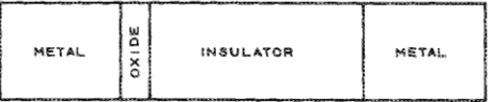
and thus interface states are no longer in intimate contact with metal states through tunneling. Thus we can have, in fact, metal-insulator-semi-conductor contact. In metal-insulator-metal structures we may have metal-oxide-insulator contacts instead of intimate metal-insulator contacts, where oxide is an insulator of wider energy band gap. In this case our structure is metal-oxide-insulator-oxide-metal. As the anode is forward biased and offers very little resistance to current, we continue to consider it as intimate insulator-metal contact. As such our structure is metal-oxide-insulator-metal (MOIM) as shown in Fig. 3.w a
METAL
-
tNSULATOR METALx 0
FIG. 3. Metal-oxide-insulator-metal structure.
Many authors9-12 have discussed capacitance versus ap-plied potential characteristics of metal-amorphous semicon-ductor contact (particularly amorphous silicon) to know impurity distribution in semiconductors. They considered quasi-Fermi level to be flat throughout the depletion region, which appears to be an incorrect assumption for intimate metal-semiconductor contact. We think that this assump-tion is valid only for metal-insulator-semiconductor-type structures with an insulator thickness of the order of 50
A
or more. This assumption needs more discussion.28 However, if the Fermi level is flat throughout the depletion layer for an applied potential even for intimate metal-insulator contacts we still can use the results here except that, in this case, Vox is zero.III. FORMULATION
We are considering a metal-oxide-insulator contact at interface. The thickness of the oxide layer is about 50
A,
so that oxide-insulator states are no longer in contact with ュ・エセ@ al states. The oxide layer is considered to be free from any kind of electrical charge. This means that the electrical field is constant throughout the oxide layer. If the oxide layer thickness is very small in comparison to the depletion layer thickness, the potential fall across the oxide layer is small and can be neglected. This is normally the case when the effective density of impurity states in the depletion layer is less than 1018/cm
3•
The impurity states are di.stributed throughout in prohi-bited energy bands in an amorphous 1nsulator. Apart from this we have energetically distributed surface states at the oxide-insulator interface. Joining these two types of imp uri-ties, the impurity density per eV at energy c at distance x
from the interface is given by
N(c,x) =Ae Kbセ@ exp( -xIR), (3)
where A" B <' and R are constants and depend on the
meth-od of fabrication of the device. The influence of a spatially nonhomogeneous trap distribution on the electrical charac-teristics has been discussed by Kao and Hwang29 and more recently by Rybicki and Chybicki. 30
In order to study the essential effects of the energetically distributed impurities, we consider R
>x,
that is, impurity density is independent of x in the depletion region. Further, we are considering the case when impurities are uniformly distributed throughout the prohibited energy band. ThusN(c,x) is constant. We denote it by No. Apart from energeti-cally distributed impurities, we are considering Nd ゥューオイゥセ@
ties/cm3
at an energy level Et which is considered to be coin-ciding with the Fermi level. These impurities can be doped impurities.
As the contact is blocking, we consider that in the
re-178 J. Appl. Phys., Vol. 68, No.1, 1 July 1990
verse-biased steady state, almost the whole of the applied potential appears across the contact. The total contact po-tential ( Vc ) is thus Vbi
+
Vapp - Vox, where Vbi is (IAJ q).Vox is the potential on the oxide layer, and in the charge-free
oxide layer is given by Vox
=
Lol<. X Eox . Lox is the thickness of the oxide layer, and Eox is the electric field in the oxide layer, which is equal to the electric field at the oxide-insula-tor contact [Ee (0)]. ThusVc
=
Vap+
Vbi - L"xEe(O). (4)If the contact potentiai at distance
x
from the oxide-insulator interface is Vex), the total positive charge density at this point isp(x) = q[ Nd - qNoV(x) ]. (5)
We are considering that contact potential Vex) is - Vc at
x = 0 and 0 at x = W, where W is the thickness ofthe deple-tion layer and q is the magnitUde of the electronic charge. In reverse-biased contact, V(x) is negative so that both types of impurities are creating a positive charge.
IV. CALCULATIONS
The distribution of electric potential and field is ob-tained through the solution of Poisson's equation, which in the present case is
d2V q
- - 2 = - - - [Nd -qNoV(x)]. (6)
dx KEo
Integrating Eq. (6) with the boundary conditions (i) for
x
=
0, Vis - Vc and (ii) forx
=
W,v
and electrical field (E) are zero, we getdV
]イkMM[イセRNkR@
V,dx
where
KI
=
q2NoiKEoand
K2
=
qNdlKEo·(7)
(8)
Integrating Eq. (7) with the boundary conditions and using
v,
= -
D, that is Vs gives the magnitude of the reversed bi-ased potential, we getEquation (9) gives the variation of the contact potential in-side the depletion layer in terms of the total contact potential on the depletion region ( Vc ) considering Vs = 0, for x = W,
the thickness of the depletion layer is given as
W
=
lI.JKI cosh-I [(K1 Vc+
K2)IKz ). (10)Using this result, Eq. (9) simplifies to
Vs
= HkRikiIサ」ッウィ{NjォセHwMクI}@
-n.
(II)Differentiating Eq. (11) with respect to x, the magni-tude of the electrical field in terms of Wor Vc is given by
dV, kセ@ [ -- ]
E.(x)= - - - ' =-4-sinh ,fk/(W-x) .
C dx
Jk;
.
(12)
Wis related to Vc through Eq. (10). The electrical field at the oxide-insulator interface (x = 0) is
(13)
The potential fall across the oxide layer is thus
(14)
The value of Ee (x) for a given Vap is obtained by solving
Eqs. (4), (10), (12), and (13) simultaneously.
The electrical charge (Q) inside the depletion region is
Using Eq. (11) for V, and integrating, we finally get
Q
= (qNd/,jk;)sinh(,jkl W). (15)Through Eqs. (13) and (15), it is easy to see that
Q
= KEoEc (0). (16)This is in accordance with Poisson's equation. The capaci-tance of the depletion region can be calculated through
(17)
v.
DISCUSSIONFirst we consider two special cases:
(i) When energetically distributed impurities are not very important, that is, qNoVc -<Nd (or kj Vc
<k
2 ): In thiscase we consider cosh x
=
1+
x2/2 and sinh クセクN@ Thus
Substituting this value in Eqs. (10) and (13), we get
W= (2VJk2 ) 1/2 = (2KEoVJqNd)li2
and
(19)
(20)
These are the same results as in intimate Schottky bar-rier with the only difference that now Vc is related to Yap
through Eq. (4). In this case Was well as Ee (0) are propor-tional to V:I2. If the contact current (I) is given through the Schottky effect that is In I ex: Ee (0)
112,
and effective trap den-sity (qNoVc+
Nd ) in the depletion region is less than 1018/ cm3, then In I will be proportional to V;/4 or (Vap
+
Vb; ) 1/4.The capacitance in this case is given by
C
=
(2qNdKr:O/Vc) In, (21)or capacitance is inversely proportional to V セQR@ or
( V ap
+
V.) bi [/2 •(ii) When energetically distributed impurities are pre-dominant, that is, qNoVc ,>Nd (or KJ Vc ,>K2 ): In this case,
179 J. Appl. Phys., Vol. 68, No.1, 1 July 1990
we can consider cosh x
=
sinh.x
セ@ eX /2 or cosh-lex) = In(2x). Thus(22)
and
(23)
or
(24)
In this case Ee (0) is proportional to
(V:
w+
Vb;) . If the cur-rent in steady state is through Schottky effect, then In Icc (V"p+
Vb;)!/2 (or V!;2 if Vap'>
Vb;)' As k\ VJk2,> 1, therefore In(2kl Vclkz) changes very slowly with Ve or Vap' Thus the width of the depletion region is almost constant.The charge inside the depletion region in this case is given by [q2 keaNo) 1/2 Vc ]. Thus the capacitance of the de-pletion region is
i.e., capacitance is almost constant as generally
Lox (q2NolkfEo) 1/2
-<
1.For the purpose of illustration of the variation of ・ャ・」エイゥセ@ cal potential and field, etc., with energetically distributed impurities, we consider the case in which Nd
=
3 X 10¹⁷ im-purities/cm3 and No varies between 1016 to 1020 impurities/ cm3 eV. The dielectric constant is considered to be 11.7, The thickness of the oxide layer is taken to be 50A.
In Fig. 4, we plot the variation of electrical potential within the depletion region for various values of Vc' In Figs. 4(a), 4(b), 4(c), 4(d), and 4(e), we consider No = 1016
, 1017,1018
, 1019, and 1020 impurities/eV em3, respectively. In Fig. 5, we have plotted the variation of potential in the deple-tion region for various values of No, considering Vc
=
3 V. We observe that for comparatively low values of qNo V<, the potential is distributed over comparatively long distances for higher values of applied potential and Vs is proportional tox'
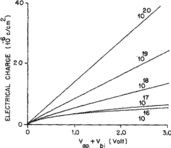
as in the Schottky barrier. For comparatively higher val-ues of qNo"v'., the potentials is distributed over almost the same distances for various applied potentials.In Fig. 6 we plot the variation of electrical charge re-leased in dielectric relaxation (Q) with applied potential for various values of No. For low values of qNo V" the electrical charge is neady proportional to V セセRL@ while for higher values it is proportional to Vap. In Fig. 7 we give the variation of capacitance with applied potential. For low values of qNo V;.,
capacitance is inversely proportional to
{v"p-,
while for higher values it is almost constant.In Fig. 8 we plot the variation of electrical field within the depletion region for an applied potential equal to 3 V. In Fig. 9 we give the variation of Ee (0) with applied potential for various values of No. In case oflow qNo Vo Ec (0) is pro-portional to V AセRL@ while for higher values it is proportional to
Val'. In Fig. 10 we plot the variation ofthickness of the deple-tion layer (W) with Va,,' For lower values of qNo Vo ' W is
proportional to vセiRL@ セィゥャ・@ for higher values, it increases
セS@
!
-'
セR@
:z w I-0 "-I-I u is z 0 °0 0 o 3V 16 N;10 IV 0.5V 0,5 1.1
-5
DISTANCE .(10 em) (a)
0.5 0.75
-5
DISTANCE .(IOem) (cl
!\-O----7>V
0.05
=3
0:::.
''''''---7>V-'
'"
1=2 zUl 1 ... i--\r---2V
l-0 "->-1 u ;:! z 0 °0
0 0.5 1.1
DISTANCE セ@ (105em 1
(b)
1'rdf---2V
QBBセセセMMoNUv@
20
N .\0
o
0.2
DISTANCE K
(Iel'
em) (d)0.1 0.15
0.4
DISTANCE .(105em)
to)
FIG. 4. Variation of electrical potential inside the depletion region for sev-eral values of contact potential (Vc )' No is 10'6, iOn, 10'8, 10'", and to20
/
eV crn3 in (a), (b), (c), (d), and (e), respectively
very slowly and can be considered as constant. These are the same results that we obtained analytically.
In conclusion, we can say that when energetically dis-tributed impurities are less important than impurities at a
16 \ ... - - - 1 0 17 .... - - - 1 0
is -·--10
19
セセMGセMMGo@
20
|MMLBGMMGGGGMZ」MMGGセ」ャP@
PTMセセMMMイセMMセセLMMセ@
o
0.5 1.0 1.2DISTANCE x (j()5cm1
FIG. 5. Variation of electrical
po-tential inside the depletion region for several values of No. Vc is 3 V.
160 J. Appl. Phys., Vol. 66, No.1, 1 July 1990
1,0 2,0
V
oP.+ Vbi (Voill
20 10
3,0
FIG. 6. Variation of electrical charge inside the depletion region with ap-plied potential for several values of No.
1.5
1.0
20
No :::10
19 10
18
セNMMMMMMMM
16
==
10
oセiMMMMMMMMMMtLMMMMMMMMMMェイMMMMMMMセL@
o
1.0 2.0 3.0Vap.+\i (Volt)
FlG. 7. Variation of capacitance with potential for several values of No.
o -' lJ.l "-.J 4,0
セ@ 1.0 a: r-o w .J W
o
4.0 B.O-6
DISTANCE (Wcml
12,0
FIG. 8. Variation of electrical field inside the depletion region for several values of No. V;.?P is 3 V.
1.0 2.0
V ap.
+
Vb' (Volt) I3.0
FIG. g. Variation of electric field at x = 0 with applied potential for several values of No.
single level, that is, qNo Vc
<
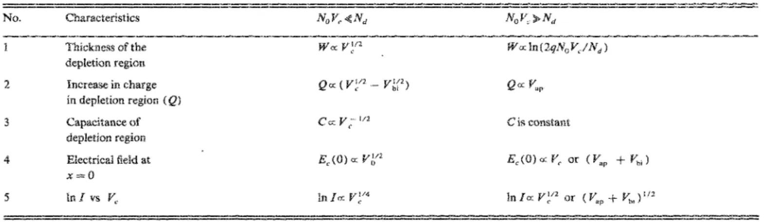
N d' the final results are more or less the same as in an intimate Schottky barrier. The poten-tial fall across the oxide region is very small in comparison to the potential fall across the depletion layer (except whenNd セ@ 1018fcm3) and the same results can be used. For Nd '$> 1018 fcm3 we can still use the results, except that we need to use Vc instead of Val" For higher values of qNo Vo the final results change significantly. In Table I we compare charac-teristics in two cases.
The capacitance of the metal-insulator contact is occa-sionally considered31-33 to be constant without considering details of the Schottky barrier. The capacitance of the con-tact can be considered constant only if energetically distrib-uted impurities are more important in the depletion region. In MIM structures, characteristics are sometimes con-sidered33--41 to be contact limited (Schottky effect) ifln 1 is proportional to V AセRN@ As per Schottky effect, In I is propor-tional to Ec (0) 1/2. Thi.s means that the field is considered uniform throughout the insulator. This is only possible when
TABLE 1. Comparison of electrical characteristit.'S of the Schottky barrier.
No.
2
3
4
5
181
Characteristics
Thickness of the depletion region
Increase in charge in depletion region (Q)
Capacitance of depletion region
Electrical field at
x=o
lnl vs V"
J. Appl. Phys., Vol. 68, No.1, 1 July 1990
Cc:: V,:-1/2
E
1,2 Qセセ@
-- 1.0 z
o
Ci
W
0:: Z
o
i=
w
...I
fu
0,5o
LA..
o
セ@
w
Z :lo: (.)
X
I-oセMMMMMMセMMMMMMセMMMMセ@
o
1.0 2.0 3.0V TV .... {Volt} (lp. ,,!
FIG. 10. Variation of the thickness of the depletion region with applied potential for several values of No.
space-charge effects are not present.34 In blocking contacts, most ofthe applied potential appears across the contact and we have a space-charge region. The space-charge effects are important and the electrical field cannot be uniform throughout the insulator. However, if energetically distrib-uted impurities are more important, we still can have
Ec (0) ex:
V:,p
and thus in I is proportional to vAセRN@ In thiscase distribution of potential is quite complicated and is not uniform. For low density of energetically distributed impuri-ties, we must have In I ex V セOT@ in blocking conta.cts.
The nonsteady-state characteristics of some metal-insu-ャ。エセイMュ・エ。ャ@ structures can be explained better by considering constant capacitance of the space-charge region.42 In the present model, the capacitance turns out to be almost con-stant, when energetically distributed impurities are more im-portant.
W 0: In (2ql\To Vj Nd )
C is constant
The results presented here are useful for interpreting the electrical characteristics of MIM structures (particularly those of amorphous material) correctly and to have a better understanding of metal-insulator-metal blocking contacts.
'F. Brawn, Progg. Ann. 153, 556 (1874).
2K. E. Peterson and D. Adler, J. App!. Phys. SO, 925 (1979).
3R. W. Berry, P. M. Hall, and M. T. Harris, Thill Films Technology (Van Nostrand, Princeton, New Jersey, 196!l).
4H. K. Henisch, Rectifying Semiconductor Contacts (Oxford University, London, 1957).
5E. H. Rhoderick, Metal-Semiconductor Contacts (Oxford University, London, 1978).
"J. Lindau and T. Kendelewicz, C. R C. Cn!. Rev. Solid State Mater. Sci. 13,27 (1986).
7J. D. Cohen and D. V. Lang, Phys. Rev. B 25,532.1 (191l2.).
sp. J. Bryant, J. M. Majid, C. G. Scott, and D. Shaw, Solid State Commun. 63,9(987).
9R. A. Abraham and P. 1. Doherty, Philos. Mag. 45, 167 (1982). lOA. S. Yapsir, P. Hadizad, T. M. Lu, J. C. Corelli, J. W. Corbett, W. A.
Lanford, and H. Bakhru, Phys. Rev. B 37,8982 (1988). I'J. J. Shian and R. H. Bube, Solid-State Electron 29,1153 (1986).
120. V. Lang, J. D. Cohen, and J. P. Harbison, Phys. Rev. B 25, 5285
(1982).
"N. F. Mott, Adv. Phys. 16,49 (1967).
.. s.
R. Pollack and J. A. Seitchick, AppL Solid State Sci. Adv. 1, 343 (1969)."C. B. Duke, Tunneling ill Solids (Academic, New York, 1969).
182 J. Appl. Phys., Vol. 68, No.1, 1 July 1990
16W. Schottky, Z. Phys. 113,367 (1939).
17J. Bardeen, Phys. Rev. 11, 717 (1947).
,"So G. Louie and M. L. Cohen, Phys. Rev. B 13, 2461 (1976).
19p. Chattopadhyay and A. N. Daw, Solid State Electron. 28,831 (1985). 20S. W. Tarasewicz and C. A. T. Salama, Solid-State Electron 27, 33 (1984). 2'1. G. Simmons and G. W. Taylor, Phys. Rev. B 5,553 (1972). 22H. M. Gupta and R. J. Van Overstraeten, J. Phys. C 7,3560 (1974).
23H. M. Gupta, J. Appl. Phys. 48, 3448 (1977).
24For example, see S. M. Sze, Physics 0/ Semiconductor Devices (Wiley, Interscience, New York, 1969), p. 371.
251. Solomon, T. Dietl, and D. Kaplan, J. Phys. (Paris) 39, 124 (1978).
2'D. G. Ast and M. H. Brodsky, J. Non-Cryst. Solids 35-36, 61! (1980).
27S. J. Fonash, J. App!. Phys. 41, 3597 (1976). 2"W. Dabrowski, Phys. Status Solidi A 165,511 (1988).
29K. C. Kao and W. Hwang, Electrical Transport in Solids (Pergamon, Ox-ford, 1981).
30J. Rybicki and M. Chybicki, Thin Solid Films 149, 261 (1987).
JIB. L. Timon, SOY. Phys. Semicond. 7,163 (1973).
32G, P. Srivastava, P. K. Bhatnagar, and S. R. Dhariwal, Solid-State
Elec-tron 22,581 (1979).
33C. M. Vodemicharov and M. B. Vodemicharov, Phys. Status Solidi A 57, 483 (1980).
MR. I. Frank and J. G. Simmons, J. Appi. Phys. 38, 832 (1967). 35G. Lengyel, J. Appl. Phys. 37,807 (1966).
"'1. T. Johansen, J. Appl. Phys. 31, 499 (1966).
37T. E. Haltman, J. C. Blair, and R Bauer, J. Appl. Phys. 37, 2468 (1966). 3"J. C. Schung, A. C. Lilly, Jr., and M. A. Lowitz, Phys. Rev. B 1, 4811
(1970).
39A. C. Lilly, Jr. and J. R. McDowell, J. Appl. Foys. 39, 141 (1968). 4Gp. L. Young, J. AppL Phys. 47, 242 (1976) .
"D. M. Taylor and T. J. Lewis, J. Phys. D 4,1346 (1971).
42M. M. Gupta, Appl. Phys. Lett. 33,778 (1978).