Abstract— The use of innovative materials is an upcoming field of 3D printing. 3D printing a wider variety of materials, provides more freedom of design and customized products. The use of chemical plating solutions enhances the rate of deposition of metallic particles onto a substrate. The removal of heavy metals from domestic and industrial waters is an important application, where in variety of sensors are employed. Nano particle based sensors have superficial sensing properties over conventional sensors, as it offers higher sensitivity in a shorter response time. The sensor materials used for detection of heavy metal ions requires to be layered in an accurate fashion and required resolution, where 3D printing could be used. The sensing materials needs thorough analysis and experimentation prior to be used by 3D printers. The compatibility to printing for chemicals involves multiple testing on their properties. The materials used for producing nanoporous gold on a metallic substrate such as copper, is analyzed. The nanoporous gold film is fabricated by immersing copper in potassium gold cyanide solution. The surface conductivity depends on the resistance of copper material after immersion for specified time, which is experimented and characterized. The pH dependence of the PGC mixed solution on resistance parameter is experimented and verified using two copper strips. The porosity is 0.07% and 0.28% for the two strips, where the grain sizes are measured to be 2.5 and 11.5 microns for strip1(32mm) and strip2 (46mm) respectively. The calculated theoretical resistance is tracked along with the measured resistance after PGC immersion experimentation. 3D printing considerations are laid out for 3D printing based on the experimentation results.
Index Terms— 3D printing, potassium gold cyanide, pH testing, nano porous gold
I.! INTRODUCTION
Metal nanoparticles have been employed as enhancers of the electro analytical signal in different sensor architectures due to their electro catalytical properties [1].
Manuscript received Aug 03, 2016; revised Aug 10, 2016. This work is performed in BITS PILANI DUBAI CAMPUS, Dubai as part of Arivarasi’s Doctoral Research.
Arivarasi A is the PhD student of (Electrical & Electronics Engineering) BITS PILANI DUBAI CAMPUS, Academic city, Dubai. P.O. BOX 345055 Phone +971 04 420 0700 email [email protected].
Dr Anand Kumar, Professor - Electrical & Electronics Department is with BITS PILANI DUBAI CAMPUS, Dubai. P.O.BOX 345055 Phone +971 04 420 0700 email [email protected]. His research interest includes VLSI, MEMS, Molecular Electronics and 3D printing.
Dr Jegatha Nambi Krishnan, Assistant Professor – Department of Chemical Engineering BITS PILANI, K.K.Birla Goa Campus, Goa. P.O.BOX 403726 Phone +91 8322580395 email [email protected]. Her research interest includes the development of Advanced materials for Electro-Chemical Systems, Bio-MEMS and Sensors.
(gold) nanoparticles have been designed with the aim of Gold nano particles are employed to improve the sensitivity of several kinds of sensors [4]. Hybrid nanomaterials containing Au enhancing the analytical response of electrochemical sensors and biosensors [1].
Nano porous gold has potential material benefits for sensor applications due to its high surface area, high electrical conductivity and reduced stiffness [7]. Electrochemical sensors utilize nano porous gold prepared using electroless plating method, which is of amperometric type. The amperometric sensor produces current signal proportional to the analyte concentration [15].
The wide variety of materials used currently for 3D printing are photopolymers, thermoplastic filaments, thermoplastic powders, metal powders, sand and binder, welding wire, plaster. The emerging materials are silicone, biomaterials, carbon fibre, regolith, ceramics, graphene and other electrically conducting materials [12].
The primary objective of this analysis is to process information based on theoretical and experimental method for the material suitability. The material preparation for 3D printing and considerations for printing PGC with suitable viscosity is analyzed. The sensor layers, once printed can then be fabricated to detect heavy metal ions in water. Experiments are conducted with the bath properties of appropriate chemical compositions and pH variations for 3D printing purpose. Chemical compounds which contribute to the suitable fluid properties are tested. The corrosion factor is to be considered for the 3D printing nozzle, which is made of brass metal.
II.! STRUCTURE OF THE NANO SENSOR
The water quality sensor includes a substrate and a copper layer, above which the nano porous gold layer is formed. Titanium epoxy is used as an adhesive to hold the copper to the substrate. Titanium has a low coefficient of thermal expansion and very low electrical conductivity and hence is suitable as an adhesive. Furthermore, Titanium epoxy bonds well with metal, copper and semi conductor wafers. The 3D printed copper layer is formed by sintering nano copper ink. The nano copper ink can be prepared by mixing Copper nanoparticles, Hydroxyl terminated polybutadiene (HTPB) and Toluene DiIsocyanate (TDI) in right proportions [14]. The sintering takes place at about 700C. Copper is corrosion resistant. Oxygen free copper [3] is used above the Titanium layer; both the copper and Titanium layers are of nanometer thicknesses [2].
Arivarasi A, Anand Kumar R, Jegatha Nambi Krishnan
Design & Material Characterization of
A.! Sensor layers
Fig 1 demonstrates the sensor layers for 3D printing, wherein the base substrate, such as Silicon is prepared and centered below the nozzle. The Titanium adhesive layer is printed on substrate. The copper layer is printed on the adhesive, where it gets set without any oxidation. The characterization of sensing materials is performed through a detailed study. The potassium gold cyanide (PGC) is sprayed using 3D printer nozzle, where nano porous gold is formed on the surface. Surface formation is performed as the final step of sensor fabrication / printing. Sensor prototype fabrication is a key step before product development [13]. The Electro less plating method is followed for the mentioned electrochemical process. Electro less plating solution is mostly in the form of plating solution [16].
Fig 1 - Schematic for fabrication of NPGF electrode using 3D printing, using a method similar to Fused filament fabrication. The nano porous gold is formed at the top of copper layer after few hours of spraying PGC as per 1(c), 1(d). The titanium epoxy is used for adhesion on top of silicon layer to copper on top, as per 1(a),1(b).
III.! PGC REACTIONS WITH COPPER
Elsner’s equation for cyanidation is used as base to define the PGC reaction with copper in the presence of oxygen and water. Gold and cyanide mixed with oxygen and water produces gold cyanide with potassium hydroxide. With sodium cyanide mixed with gold in aerated environment, produces sodium gold cyanide. The gold undergoes reduction process. It is experimentally verified using a copper strip. Nanoporous gold is formed on the copper surface, which is characterized using microscopic study. The plating speed or rate depends on the pH of the composition at a particular temperature. The water soluble gold compounds containing cyanide ions readily dissociate for gold to adhere on a substrate, when used at a particular pH. Cyanide is well known to dissolve gold in the presence of oxygen and alkaline aerated solutions [17]. Usually the range of concentration of gold compounds in plating solution is from 1 to 100 grams per litre. There is a relationship between pH of the solution and the gold plating rate [5].
For 5 gr/l PGC in water, when mixed with zinc chloride and ammonium chloride proportionate to corresponding composition in [5], the gold plating rate increases after pH of 9. For the composition containing ammonium chloride only, the gold plating rate increases after pH of 12.5, performed at 900C for both cases [5]. It is noted that the gold plating rate can be obtained of 2.2µ/hr. at pH 8, 4 µ/hr. at pH 9, 7.5 µ/hr. at pH 10 can be obtained at 900C [5].
IV.! EXPERIMENTAL STUDY &ANALYSIS OF PGC REACTIONS FOR PH VARIATIONS
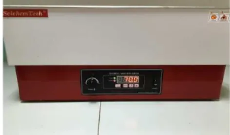
In the experiment, a PGC solution of 15ml is prepared using 2.25g of PGC is made in a beaker and stirred with a glass rod till completely dissolved. The PGC solution is then heated in a digital water bath at 70ºC as shown in Fig 2. The test tube containing the PGC solution is mixed with 0.2g of KOH, 0.2g of CaCO3, 0.2g of NH4CL, 0.2 ml of NH4OH is indirectly heated in the bath. The PGC solution mix is heated for 30 minutes before immersing the Copper strip1 in the solution. The resistance of the copper strip is then measured during digital multimeter. The resistance of the strip is also measured subsequently after 30 minutes and 90 minutes [2].
Fig 2 – Double layered heating system for heating PGC solution.
Two PGC solutions are prepared for the two copper strips of different dimensions to be tested. The pH is verified for two different PGC solutions at 440C and 33.50C, as in Table 1. The pH meter SCT-BEN, ScichemTech is used for experimentation. pH of distilled water is measured to be 6.98 at room temperature.
Table 1 –pH values at different temperatures Solution pH at 440C pH at 33.50C
PGC1 11.57 11.51
PGC2 11.44 11.40
The dimensions of two copper strips are given in Table 2 and the theoretical resistances are calculated. The resistance of copper strip is calculated using the formula R = ρ.%
& , where ρ = Resistivity of copper in ohms meter, L = Length of the copper strip in milli meters, A = cross sectional area of the strip in milli meter square. The theoretical resistance values are 20 micro ohms (strip1) and 0.014 ohms (strip2) respectively.
Table 2 – Copper Strip dimensions, properties for pH based PGC testing Strip1 – Electrode copper
Length =32 mm; Width = 0.2 mm; Thickness 1.32 mm; Strip cross sectional area = 0.264 mm2
Resistivity of copper = 1.68 x 10⁻⁸ Ohms m Strip 2 – Pure copper (purity greater than 99.95%) Length = 46 mm; Width = 12 mm; Thickness 2.8 mm; Strip cross sectional area = 552 mm2
PGC1 is used for testing copper strip1 (Electrode copper of smaller dimension, length = 32mm). PGC 2 is used for testing copper strip 2 (Pure copper of comparatively larger dimension, length = 46 mm). The experiment is carried out for two PGC and copper strips respectively. Table 3 provides the experimental steps followed in the laboratory.
Strip1(length = 32mm) immersed in PGC1 after bath heating temp of 760C and inside liquid temp to 440C.
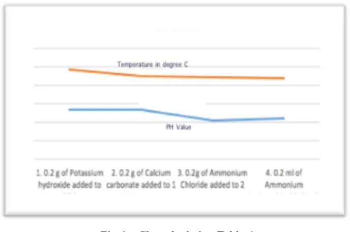
Table 3 – The pH value readings for the corresponding temperatures of material with specified chemical alkaline compositions to PGC solution. Data given for PGC1/Strip1 (l=32mm)
Material added for solution pH Value Temp (0C) 1. 0.2 g of Potassium hydroxide
added to PGC
12.96 31.96
2. 0.1g of Potassium hydroxide added to 1
13.17 27.1
3. 0.2 g of Calcium carbonate added to 2
13.27 26
4. 0.2g of Ammonium Chloride added to 3
10.70 21.8
5. 0.2 ml of Ammonium hydroxide added to 4
11.17 22.1
Fig 3 – Chart depicting Table 3
Strip2 (length = 46mm) immersed in PGC2 after bath heating temp of 760 C and inside liquid temp to 440C. The two strips’ values are characterized using microscopic study for the grain sizes, porosity values and resistances measured pre – post stages of PGC immersion.
Table 4 – The pH value readings for the corresponding temperatures of material with specified chemical alkaline compositions to PGC solution. Given for PGC1/Strip1 (l=32mm)
Material added for solution PH Value Temp (0C) 1. 0.2 g of Potassium hydroxide
added to PGC
13.29 24.2
2. 0.2 g of Calcium carbonate added to 1
13.26 22.3
3. 0.2g of Ammonium Chloride added to 2
10.52 22
4. 0.2 ml of Ammonium hydroxide added to 3
10.88 21.8
Fig 4 – Chart depicting Table 4
A plating solution containing a water soluble gold compound ion, is added with ammonium hydroxide or a caustic alkali such as sodium hydroxide or potassium hydroxide, to adjust or control the hydrogen exponent value [5]. The pH is adjusted, making the solution alkaline. In the electroless plating of gold solution, gold ions in the plating solution gets reduced as per the following equation:
'()*+ , → ()'''''''''''''''''''''''''''''''''''''''''''''''''''''''''''''''''''''' − (1)
It is found that, for PGC1- Strip1 (length = 32mm), the pH value is maintained high for potassium hydroxide mixed with PGC, compared to consecutively adding ammonium hydroxide. Adding calcium carbonate and ammonium chloride reduces the pH to 13 and 10, making lesser alkaline at 260 C and 21.80C, as given in Fig 3
It is found that, for PGC2-Strip2 (length = 46mm), the pH value decreases from highly alkaline to just alkaline, when ammonium chloride is added, at 220C, as given in Fig 4.
It is a proven fact that gold plating rate of 2 microns/hr is obtained by using the plating solution having pH as 10, whereas when plating solution using pH as 7 , the gold plating rate is 0.3 microns/hr [5]. Hence making the PGC solution with pH as alkaline is important. Buffer agent, such as ammonium chloride to adjust pH is not always important. It is evident from the experimental results.
Potassium gold cyanide gets dissociated into Potassium and gold cyanide [()(23)4-] , where in gold cyanide gets dissociated into ()5and 2235and subsequently, equation (1) gets effected. The most important ion for this deposition process is [()(23)4-] [8].
It is evident that, adding potassium hydroxide can make the PGC solution highly alkaline, whereas ammonium hydroxide can make the PGC solution have pH from 10-11 range. The effect of calcium carbonate is that, it can reduce final conductivity, and hence the addition could be on need basis. It reduces cathodic efficiency as well [6]. The suitable chemical combinations are considered for 3D printing / spraying PGC, which is oriented to the CAD design geometric limits.
V.! METALLURGICAL STUDY OF COPPER STRIPS REACTED WITH PGC SOLUTION
Strip1 (l=32mm)
Strip2 (l=46mm)
Fig 5 – Pictures of the copper strips after 90 minutes of immersion into PGC mixed alkaline solution.
The pictures (Fig 5) of copper strips used for this experimental study is of lengths 32 and 46 mm, thicknesses of 1.32 and 2.8 mm, are provided and observed after immersion in PGC. As, the two strips are of different dimensions, they are tested for resistance variations and nano porous gold formation surface structures as a result of PGC/PH experimentation. The variation in porosity and phases are noted to measure the conductivities in future. The picture is taken through metallurgical microscope, analyzed through Envision 5.0 software.
Fig 6 – Image of a metallurgical microscopic picture, which belongs to Strip1(32mm) after 90 minutes of immersion in slightly heated PGC mix solution having materials of Table 3. Image captured and processed through Envision 5.0 software
Fig 6 demonstrates the surface micro structure of strip1, where the nanoporous gold formation is seen. The surface gets continuously modified, when immersed in alkaline PGC solution due to the potassium gold cyanide reaction with electrode copper.
Fig. 7 - Image of a metallurgical microscopic picture, which belongs to Strip2 (46mm) after 90 minutes of immersion in a heated PGC alkaline mix solution having material compositions of Table 4. Image captured and processed through Envision 5.0 software
Fig 7 provides a picture seen through metallurgical microscope of strip2, after 90 minutes of PGC mix immersion. The medium is maintained alkaline by adding the suitable chemical compositions and heated bath to increase the deposition rate. The formation of gold nano particles are
seen after 30 minutes of immersion. The resistance is expected to be comparatively lesser than strip1.
A. Grain Size
Nanoporous gold exhibits polycrystalline microstructure with few micron grain size [9]. Here average grain size is considered for analysis, calculated using circular intercept method and Hayn Intercept methods, as per Table 5. The average grain size is 2.5 microns for strip1 and 11.5 microns for strip2, considering the inherent dimensions. The grain could be drawn and measured in Envision software 5.0. Instead, the grain areas are selected automatically by the software and measured for average grain size. Grain size is the diameter size of each grain, present in the target space. Table 5 – Grain size measurement through metallurgical microscope and Envision software 5.0. Calibration of 24 µm/pixel; Magnification 40X; Unit – Microns
Strip1(l=32mm) ASTM Standard E112 Average Grain Size 2.5 Total Circle length(mm) 2.62 No. of Intercepts 18.5
Strip2(l=46mm) ASTM Standard E112 Average Grain Size 11.5 Total line length(mm) 1.85 No. of Intercepts 329.5
B. Porosity
The porosity factor also defines conductivity, through roughness factor and surface to volume ratio. Metallic porous (gold) films, is of particular interest due to its chemical stability and unique surface chemistry [18]. Porous gold films are used for better detection and perform as ideal electrodes.
Larger pores in a material facilitate mass transport, whereas the smaller pores increase surface area drastically [10]. Nanoporous gold has numerous pore structures, which actuates the chemical process [10]. In a few applications, the gold nano particles are functionalized with other metal particles to increase the conducting, mechanical and optical properties of porous structures [11]. Porosity enhances the catalytic activity [18].
The porosity count is 182 for strip1(l=32mm) and 693 (l=46mm) for total porosity area% 0.07 and 0.28 respectively. With the total area selected being same, the porosity count is larger for strip2, as interpreted from Table 6.
C. Phases
Phases measurement represents the number of material composition present as per the microscopic study. Strip1 has major copper composition of 87.33%, whereas Strip2 has 96.43% and the pictorial representations attached in Table7.
Table 6 – Porosity measurement for the two strips for the same total area Strip1 (l=32mm)
Total Field count 1 Total Porosity count 182
Total Area 284621 Total Porosity Area 186 Total Porosity Area
% 0.07
Length - Smallest 1 Length - Largest 5 Length - Average 1
Strip2 (l=46mm)
Total Field count 1 Total Porosity count 693 Total Area 284621 Total Porosity Area 807 Total Porosity Area % 0.28
Length - Smallest 1 Length - Largest 5
Table 7 –Phase measurement for the maximum material found, using metallurgical microscope and Envision software 5.0
Strip1(l=32mm)
Area 248551 microns Area% 87.33%
Strip2(l=46mm) Area 0.270 microns Area% 96.43%
D.Particle Distribution
The strip1 and strip 2 selected features statistics are provided below. The feature which is different unique structures of the particle is measured for its length, width and circumference. The total features are 2783 for strip1 and 3101 for strip2. This is for a particular microscopic spot. This implies the presence of multiple features on the surface of PGC mix reacted copper. The feature selection is more for larger area strip, as per Table 8.
Table 8 – Particle analysis report for the two strips under experimentation Particle Analysis Report
Strip1(l=32mm) Strip2(l=46mm)
Total Field count 1
Total Feature count 2783
Total Feature Area 334135
Total Area 284621
Total Feature Area % 117.4
Min Feature area 1
Max Feature area 260994
Min Feature Length 1
Max Feature Length 615
Min Feature Width 0
Max Feature Width 461
Min Feature Circ 0
Max Feature Circ 1
Total Field count 1
Total Feature count 3101
Total Feature Area 266696
Total Area 284621
Total Feature Area % 93.7
Min Feature area 1
Max Feature area 222349
Min Feature Length 1 Max Feature Length 615 Max Feature Width 461 1
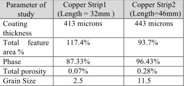
The consolidated table with measured values from metallurgical microscope/ Envision 5.0 is provided in Table 9.
Table 9 – Consolidated parameter values studied from envision 5.0/metallurgical microscope under 40X magnifications.
Parameter of study
Copper Strip1 (Length = 32mm )
Copper Strip2 (Length=46mm) Coating
thickness
413 microns 443 microns Total feature
area %
117.4% 93.7%
Phase 87.33% 96.43%
Total porosity 0.07% 0.28%
Grain Size 2.5 11.5
Even though the two strips are different in feature sizes, there is a considerable increase in porosity factor and grain size comparing both for a more or less similar coating thickness. The phase of material seems more in strip2. Higher porosity implies enhanced conductivity literally. Electrical conductivity of thin films is a function of its thickness [19]. Grain sizes are formed to be higher in strip2,
which contributes to higher conductive nature, considering thickness of strip.
VI.! RESISTANCE MEASUREMENTS
Table 10 demonstrates the measured resistances before immersion into PGC alkaline mix solution. Digital multimeter was used for measurement, where the copper strips exhibit 220 milli ohms and 760 milli ohms, based on resistivity and dimensions of the copper strips.
Table 10 – Measured resistances using digital multimeter for the two strips, having different thicknesses, lengths.
Description Strip1(l = 32mm) Strip2 (l=46mm) Before
immersion
0.22 ohms 0.76 ohms
The resistances measured after 30 and 90 minutes implies higher conductivity factor and reduced resistances due to the PGC mix reaction with the copper strips. The addition of alkaline compounds maintained the pH of PGC solution, where in calcium carbonate compound deposits on the strip are seen at, which might reduce the further reaction rate. The further addition of acidic compounds might reduce the pH rate, which is avoided in the experimentation, as it might release toxic hydrogen gas. Table 11 provides the resistances measured for two strips immersed into PGC mixed with alkaline compounds. After 90 minutes strip1 of length 32mm shows slightly lesser resistance / higher conductive nature, compared to strip2 with length 46 mm and thickness 2.8mm. The resistance formula indicates, as the area decreases and length increases resistance value is increased. After 30 minutes, this is proved as per Table 11.
Table 11 – Measured resistances using digital multimeter for the two strips, having different thicknesses, lengths
Description After 30 minutes
After 90 minutes PGC solution with Electrode
Cu strip 1 (l=32mm) 0.15 ohms 0.10 ohms PGC solution with pure Cu
strip 2 (l=46mm)
0.14 ohms 0.13 ohms
VII.! 3DPRINTINGCONSIDERATIONSTOPRINT PGC
The three dimensional structure for a low viscosity material can have a considerably lower z axis height with the print bed alignment. Factors to be considered are the temperature, composition, flow rate at start and after extrusion, drop size, pressure. Temperature conditions are to be maintained through the resistive heating setup for PGC extrusion through 3D printing. The PGC is sprayed on copper surface, where the immersion characteristics and spraying method results in similar electrical performances with controlled droplets at a constant rate. The surface roughness, porosity and grain sizes of the substrate is maintained as expected to maintain the conductivity and fine tune selectivity, sensitivity factors of the 3D printable sensor.
VIII.! CONCLUSION
to Fused Deposition Modelling. PGC reacts with copper at the surface to form nano porous gold, using Electro less plating with the pH factors affecting the alkalinity of the solution. Alkalinity in turn impacts the plating rate. The viscosity and surface tension are set while preparing for printing. The porosity is 0.07% and 0.28% for the two strips, where the grain sizes are measured to be 2.5 and 11.5 microns for strip1(32mm) and strip2 (46mm) respectively. The metallurgical microscopic study was performed using Envision 5.0 software. The experimental results are tabulated and compared. 3D printing considerations for printing PGC are laid out, for future research.
ACKNOWLEDGMENT
The authors would like to acknowledge BITS PILANI DUBAI CAMPUS, Dubai, UAE for the lab facilities provided and Dr. Jegatha Nambi Krishnan, BITS PILANI GOA CAMPUS, GOA, INDIA for the support on context.
REFERENCES
[1]! Pumera, Martin, ed. Nanomaterials for electrochemical sensing and biosensing, CRC Press, 2014.
[2]! Suprabhat Bhagavathula, Joshi Manasi Satchit, Sutapa Roy Ramanan and Jegatha “ Fabrication And Characterization of Electroless Plated Nanoporous Gold Film Electrode Electrode", International Conference on New Frontiers in Chemical, Energy andEnvironmental Engineering (INCEEE-2015), NIT Warangal, India, 2015.
[3]! Patricia Schroeder, Johnson County Community College, “Experimenting with Copper(II) Solutions” available: www.terrificscience.org/lessonspdfs/copper(I)solutions.pdf
[4]! Paul A. Kohl, Electro deposition of gold, 2010
[5]! Inaba, Yoshiharu, and Toru Kawanobe. "Method for electroless plating gold directly on tungsten or molybdenum." U.S. Patent No. 3,993,808. 23 Nov. 1976.
[6]! Fletcher, Augustus, David N. Cockayne, and William L. Moriarty. "Gold plating bath containing tartrate and carbonate salts." U.S. Patent No. 4,465,564. 14 Aug. 1984.
[7]! Seker, Erkin, Michael L. Reed, and Matthew R. Begley. "Nanoporous gold: fabrication, characterization, and applications." Materials 2.4, pp.2188-2215, 2009
[8]! Paul A. Kohl, Electro deposition of gold, 2010
[9]! Mameka, N., Wang, K., Markmann, J., Lilleodden, E.T. and Weissmüller, J., Nanoporous Gold—Testing Macro-scale Samples to Probe Small-scale Mechanical Behavior. Materials Research Letters, 4(1), pp.27-36, 2016.
[10]!John W. Overcash Advances in Nanoporous Gold Synthesis, Literature Seminar November 5, 2009.
[11]!Shaban, M., Hady, A.G.A. and Serry, M., 2014. A new sensor for heavy metals detection in aqueous media. IEEE Sensors Journal, 14(2), pp.436-441, 2014.
[12]!Gibson, Ian, David W. Rosen, and Brent Stucker. Additive manufacturing technologies. New York: Springer, 2010.
[13]!W. Gopel, J. Hesse, J.N. Zemel, Micro and nano sensor technology/ trends in sensor markets, 2008.
[14]!Wang, Qisui, Xia Chen, and Jing Xiao. "Synthesis of Cu nano- particle in toluene used for conductive ink with a binder of polyurethane." Journal of Wuhan University of Technology-Mater. Sci. Ed. 28.6, pp.1246-1250, 2013.
[15]!Stetter, Joseph R., William R. Penrose, and Sheng Yao. "Sensors, chemical sensors, electrochemical sensors, and ECS." Journal of The Electrochemical Society 150.2, 2003
[16]!Dunleavy, Michael, Sajad Haq, and Martyn John Hucker. "Electro less metal deposition for micron scale structures." U.S. Patent No. 9,260,783. 16 Feb. 2016.
[17]!Amjadi, Mohammad, Javad Hassanzadeh, and Jamshid L. Manzoori. "Determination of cyanide using a chemiluminescence system composed of permanganate, rhodamine B, and gold nanoparticles." Microchimica Acta 181.15-16, pp.1851-1856, 2014.
[18]!Zhang, Renyun, and Håkan Olin. "Porous gold films—a short review on recent progress." Materials 7.5, pp. 3834-3854, 2014.
[19]!Salvadori, M. C., et al. "Measurement of electrical resistivity of nanostructured platinum thin films and quantum mechanical estimates." Journal of Metastable and Nanocrystalline Materials. Vol.