A Protection Circuit for DC-DC Converter
with Voltage Doubler
D.Elangovan #1, A.Gopi *2, Dr.R.Saravanakumar #3
#
Assistant Professor (Senior), School of Electrical Engineering, VIT University Vellore, Tamilnadu, India
1
*
Research Scholar, School of Electrical Engineering, VIT University
2
#
Professor, School of Electrical Engineering, VIT University Vellore, Tamilnadu, India
3
Abstract-This paper proposes a method to obtain a protected voltage gain by employing a protection circuit for the voltage doubler or multiplier circuit in an isolated tyde DC-DC Converter. The entire set up consists of a phase shift converter with a protected bridge/voltage doubler rectifier on the output side. The operating frequency of the phase shift converter is 20-25kHz (depending on the requirement of the application) which is high enough to improve the efficiency. Ferrite core transformer is used in place of ordinary air core transformer, which is small in size with number of turns of the transformer is reduced and the overall power density is increased. The doubler circuit consists of electrolytic capacitors, which are rated at 400V in order to comply with IEC65 requirements. This paper proposes an “electrolytic capacitor protection circuit”, which enables the voltage rating of the electrolytics to be reduced to 250V. This circuit results in cost savings of more than 50% in the price of the electrolytic filter capacitors. The circuits were simulated using PSPICE SOFTWARE and the following results were obtained. For an input voltage of 200V, an output of 200V and 400V were obtained in bridge mode and doubler mode respectively.
Keyword- DC Direct Current, Full wave rectifier,Voltage Doubler Rectifier, protection circuit.
I. INTRODUCTION
In many applications power density is an important criterion [1-4]. The demand for decreasing cost and volume leads to increasing power density [3]. Earlier it has been proposed that voltage doubler and current doubler plays an important factor in improving power density [1-2]. In this paper phase shift converter circuit with transformer and full wave rectifier replaced by current doubler rectifier is used so as to enhance the power density at lower cost. The voltage doubler is also simulated in the same way. This paper deals with some basic background in phase shifted timing fundamentals of the synchronous rectifier [5]. Switched mode power supplies are used, as they offer designs that are compact, light, and operate over a wide voltage range. With large power requirements, a voltage doubling circuit is generally required for multi voltagesets. The most expensive components in the voltage doubling circuit are the electrolytic capacitors, which are rated at 400V in order to comply with safety requirements. The 400V rating is required to ensure safe operation under fault conditions. Under normal operating conditions, a voltage rating of 250V is adequate. This paper proposes a novel approach to meet the safety requirements, while using 250V electrolytics. This is achieved with an overvoltage protection circuit, which activates when the voltage across an electrolytic exceeds its safe operating voltage. The main benefit of using this circuit is to reduce cost. High voltage electrolytics are very expensive components. Electrolytics rated at 400V can be more than double the cost of the ones rated at 250V.
II.WORKING OF PHASE SHIFT CONVERTER WITH VOLTAGE DOUBLER
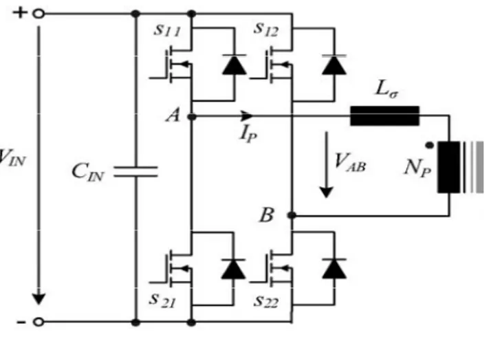
Fig 1. Phase Shift Converter
A voltage doubler circuit is shown in Fig 2 along with the phase shift converter on the primary side of the transformer. We can think of it as two half-wave rectifier circuits in series. The circuit operates in doubler mode when the mains voltage is in the range of 90 VAC to 140 VAC This corresponds to a DC voltage of 127V to 197V across each electrolytic The IEC 65 requirements are met when either electrolytic short circuits, as in this case there is a direct short across the mains, which will blow the mains fuse. If one of the electrolytics is open, no dangerous over -voltage occurs. The above information shows that the maximum voltage in the doubling mode is 190V across each electrolytic. With this one could easily conclude that a 200V electrolytic would be a good choice for practical use, as it provides 1OV derating. But one must consider the bridge mode of operation. In this mode of operation, the two electrolytics are connected in series, and when taking component tolerances into account, which are typically of 20%, the voltage across the capacitors can be divided in the ratio 60:40. This ratio is derived with the aid of equation (1). This could result in a voltage of up to 234V appearing across one of the electrolytics. Allowing for a derating of about 1OV, which is a rule of thumb for high voltage electrolytics, a voltage rating of 244V is required. The nearest possible safe value is 250V.
Vc1=Vpeak × C1 [1]
C1+C2
Vout = 2 x Vin [2]
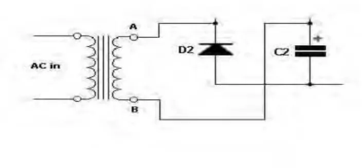
Fig 2. Phase Shift Converter with Voltage Doubler
Fig 3. Mode 1 operation
Mode 2: During the negative half-cycle the other diode (D2) conducts negatively to charge the other capacitor (C2). The voltage across the combination is therefore equal to twice the peak voltage. In this type of circuit we have to assume that the load does not draw a significant charge from the capacitors.
Fig 4. Mode 2 operation
III.WORKING OF PHASE SHIFT CONVERTER WITH BRIDGE RECTIFIER
The circuit will operate in bridge mode as shown in fig 5 at the high end of the mains voltage, which is in the range 160 VAC to 276 VAC. The DC voltage across the electrolytics is in the range 226 VDC to 390 VDC. The DC voltage can be calculated with equation (3). The 390 VDC stipulate the 400V rating of the electrolytics. This is due to the IEC 65 requirements, which requires that the set must be safe to operate under fault conditions, whereby either of the two series electrolytic may be either short or open circuit. An open circuit does not affect the safety of the set, merely its performance. But if either of the electrolytics is short, the full 390V appear across the good capacitor. Therefore, the electrolytics are rated at 400V. This would at first glance appear to be a good and simple solution to the IEC 65 requirements. If electrolytics rated at 250V were used, and one of them were to go short circuit, an unsafe condition would exist for the other one. The electrolytic would get hot and vent. The heat generated by the over stressed electrolytic could be a potential fire hazard especially in the consumer electronics industry, where the PCBs are made of card board based material.
Vcap = Vpeak (2)^1/2 [3]
Fig.5 Full Bridge with Bridge rectifier
Fig.6 Input voltage Vs Output voltage in different modes
IV.WORKING OF PROTECTION CIRCUIT
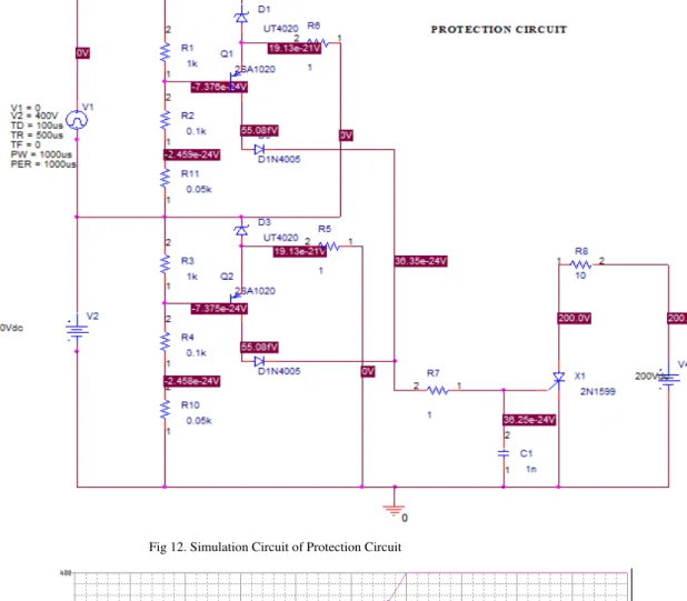
This circuit uses a transistor as a voltage comparator asshown in fig 7. The zener diode in the emitter circuit is used as a reference, which biases the transistor such that below the trigger voltage, the transistor is just off. As the voltage on the cathode of the zener moves toward the trigger level, the base voltage moves up a lesser amount. Once the trigger level is reached, the differential voltage between base and emitter is large enough to turn the transistor on. When the transistor is switched on, the crowbar circuit consisting of the SCR is triggered. This in turn blows the mains fuse. The crowbar is placed after the mains filter circuit. The resistance of the mains filter, which is of a few ohms, provides some current limiting for the crowbar circuit. The trigger point can be calculated with equation (4).
VTrg = ( VBE + VZ ) RT/R1 [4]
where,
RT =R1+R2+R3
Fig.7 Protection circuit
V.SIMULATION RESULTS
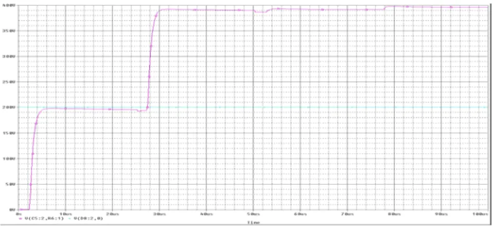
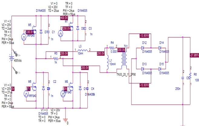
The circuits are simulated in PSPICE software. The circuit simulation of phase shift converter with voltage doubler and the output waveforms are shown in fig 8 and fig 9 respectively. The observations from the simulation output waveform is tabulated in table 1.
TABLE I
Parameter Values
Input voltage 200V
Transformer primary turns 100
Transformer secondary turns 100
Fig 8. Simulation circuit with VDR
Fig 9. Output Waveform with VDR
The circuit simulation of phase shift converter with bridge rectifier and the output waveforms are shown in fig 10 and fig 11 respectively. The observations from the simulation output waveform is tabulated in table 2.
TABLE II
BRIDGE RECTIFIER PARAMETERS
Parameter Values
Input voltage 400V
Transformer primary turns 100
Transformer secondary turns 100
Fig 10. Simulation Circuit with Bridge Rectifier
The circuit simulation of the protection circuit and the output waveforms are shown in fig 12 and fig 13 respectively. The SCR gets triggered when the voltage crosses the value predetermined using the resistors and the biased zener diode as a straight line can be noted which represents that the SCR is triggered.
Fig 12. Simulation Circuit of Protection Circuit
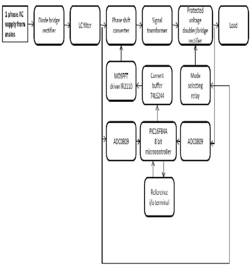
The hardware for the proposed circuit can be implemented process is shown in fig.14
Fig 14. Block diagram of Hardware Implementation process
VII.HARDWARE MODEL
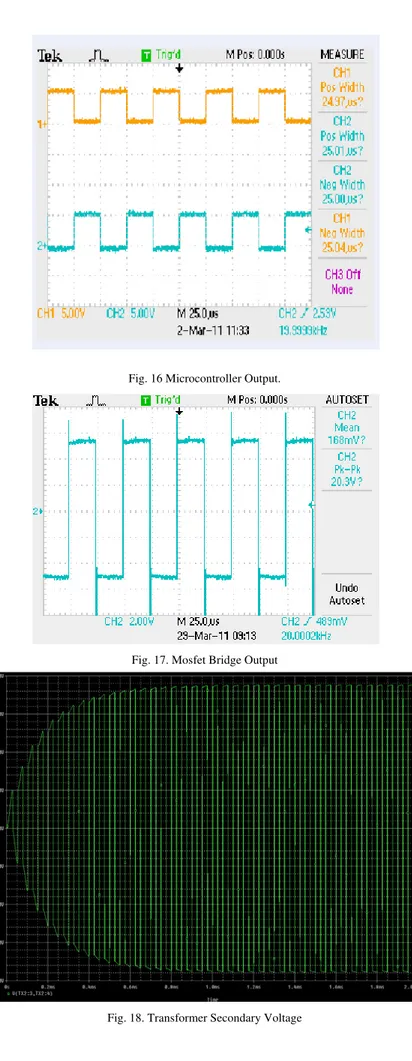
The hardware is implemented by the hardware implementation block diagram and the results of the hardware are compared with theoretical and simulation results. The hardware model is shown in fig 15 and various results are shown in fig 16 to 20.
Fig. 16 Microcontroller Output.
Fig. 17. Mosfet Bridge Output
Fig. 19 VDR output on load condition
Fig. 20 Current in Secondary of Transformer
The observation of the hardware model is tabulated in table 3.
TABLE III
When the input voltage is increased beyond 270V the voltage across each capacitor in voltage multiplier increased beyond 250V and the SCR in protection circuit is triggered and the circuit got tripped protecting the circuit
VIII. CONCLUSION
Operation on the primary side, including the duty cycle is unchanged. There is no need for centre tapping
Parameter Values
Input voltage 200V
Transformer primary turns 100
Transformer secondary turns 100
been reduced to 100 turns and for an input of 200V we can obtain a voltage of 400V from the voltage doubler, for the reduced transformer size. The core losses are considerably reduced so that the efficiency increases. The advantages of VDR are that it eliminates the need for implementing transformers with large number of turns. This enhances the compactness of the circuit which enhances the efficiency and performance considerably. Thus by implementing the VDR according to the industrial needs maximum power density and high efficiency at a low cost is achieved.The protection circuit is simple, and can be designed from standard low cost components.
The cost of this protection circuit, including two 250V electrolytics, is less than the cost of one 400V electrolytic. When the voltage is increased beyond 250V (in experiment it was 276V) the voltage across each capacitor of the voltage multiplier increased above 250V and the circuit got tripped and the capacitors are protected.This includes the extra assembly cost. Whilst it may not be as elegant a solution as using 400V electrolytic capacitors, it is by far a more economic solution. If care is taken in the rating of this circuit, reliability of the set will not be adversely affected as there are no components being stressed.
REFERENCES
[1] D.Elangovan, P.D.Dharmesh, V.Ashwini, ‘Power Density Maximization of DC-DC Converter’ in IEEE proceedings IICPE (2010), Vol. 3, No. 31, pp 31.
[2] Juergen Biela, Member, IEEE, Owe Badstuebner, StudentMember, IEEE, and JohannW. Kolar, Senior Member, IEEE, (2009), ‘Impact of Power Density Maximisation on Efficiency of DC-DC Converter Systems’, IEEE Transactions on Power Electronics, Vol. 24, No. 1. [3] Lin B.R., Huang K. and Wang D., (2005) ‘Analysis and Implementation of Full Bridge Converter with Current Doubler Rectifier’, in IEEE
Proceedings Electric PowerApplications, Vol.152, No.5, , pp.1193-1202.
[4] Teren, A., Feno I., Spanik P., (2001) ‘DC-DC Converters with Soft (ZVS) Switching.’ In Conf.Proc. ELEKTRO 2001, section –Electrical Engineering. Zilina,pp.82-90.
[5] Mozar, S., Elcap Over Voltage Protection Circuit, Philips Singapore - CTV Development, Philips Internal Report, VDEVlOO814, 1994 [6] Mozar, S., van Bodegraven, T., Philips Corporate Patents and Trademarks, Over-Voltage Protection Circuit, European Patent Application,
Filling Number 9520040 1.8, February 1995.
[7] Pressman, A., Switching and Linear Power Converter Design, Taiwan. 1977.
[8] Philips Consumer Electronics, Derating Guidelines for Application of Components, UAW-0380, Philips Internal Publication, February 1988.