Available Online at www.ijecse.org ISSN- 2277-1956
Design, Analysis and Implementation of a new
topology of multi phase synchronous buck converter
under current mode control
Nittala S K Sastry (P G Student) 1 , Dr. Swapnajit Pattnaik (Asst. Professor) 2
1 2 Department of Electrical Engineering 1 N I T Raipur 2 N I T Raipur
Email- [email protected], [email protected]
Abstract- This paper presents a new PWM Multi phase DC-DC converter under current mode control with an auxiliary circuit which provides zero voltage switching in order to meet the power supply requirements of the processors of modern electronic equipments like laptops, mobiles, and PDAs etc which require more than 70 A current, lower voltage and better transient response.The multi phase topology benefits in high current, good efficiency and better current transient response. High current multi phase buck converters found applications in advanced data control, solid state lasers, communication equipment and Pentium processors etc. In this paper designed of three phase DC-DC converter 100W, 12V/1V under current mode control is discussed in detail and the simulation results are presented to support the theoretical analysis.
Keywords – DC-DC, PWM, Multi Phase, ZVS
I.INTRODUCTION
In today’s consumer market there is a great demand on battery operated portable devices like mobiles, laptops and PDAs etc [Ashis Mity et al]. But now in these days as laptop and mobile users expect more features and long battery life, the processor current has to increase to response the demanding. To reduce the power dissipation, it is very common to start and stop the operation during the periods of inactivity [Y.Jang et al].The advantage of multi phase topology is it can provide excellent transient response, high current and good efficiency. The multi phase buck converters are generally powered from a 12V supply. In the conventional multi phase buck converters it is very difficult to get continuous conduction and equal current sharing after a certain level of frequencies. In the open loop topology of the proposed multi phase buck converter in this paper, even a small variation in the input parameters like input voltage, duty cycle and load values etc will cause a significant variation in the output inductor currents and as a result the ripple in the output voltage is going to be very high [X.W.Zhou et al]. To avoid this problem there should be some control mechanism in the circuit to control the variations in the output inductor currents and load voltage. Generally current mode control will be preferred over than voltage mode control because of its advantages like easy compensation, good performance in both continuous and discontinuous modes of operation etc [R.B.Ridley et al].
II.DESCRIPTION OF THE NEW TOPOLOGY OF THE MULTI PHASE SYNCHRONOUS BUCK CONVERTER UNDERCURRENT MODE CONTROL
The circuit diagram of the new proposed circuit will be as shown in Figure 1
Figure 1: Circuit diagram of the new topology of multi phase synchronous buck converter under current mode control
In the current mode control of the circuit proposed in figure 1 consists of an S R flip flop with an XOR gate connected to feedback path by the PID controller and a relational operator. An auxiliary switch is used to reduce the switching losses across the main switches and the current stress across the semi conductor switches. Here the SR flip flop with XOR gate acts as driver for the MOSFETs in each phase.
Theory of operation:
The circuit operation is similar to all phases. So only the operation for first phase is described in this paper.
Prior to t=t0, the synchronous switch S4 will be turned on while the main switch S1 is off. At t=t0, the auxiliary switch S7 will be turned on which realizes zero current turned on as it is in series with the resonant inductor Lr. During this stage iLr rises and current iD4 through body diode of switch S1 falls simultaneously at the same rate. Resonance occurs between Lr and Cs1 (charged previously). This mode ends at t=t1, when iLr reaches I0/3 and iD4 becomes zero. The body diode D4 is turned off with ZCS.
The diode DS1 starts conducting at the instant when body diode DS4 is turned off. At t = t1, iS7 = iLr = I0/3. In this interval, capacitor CS1 forced to conduct body diode of main switch S1. This mode ends with turned on of main switch S1 under ZVS [Y.Panov et al]. And the mains witch S1 will be turned off as per required duty cycle.
This operation is repeated for second and the third phase.
current mode control
III.FEATURES OF THE NEW TOPOLOGY OF PROPOSED MULTIPHASE SYNCHRONOUS BUCK CONVERTER
The special features of the new topology of multi phase buck converter are All the active and passive semi conductor devices are turned on and off under exact ZVS and/or ZCS.
1. Constant and high frequency of operation (1 MHZ).
2. Equal current sharing is possible even at very high frequencies which is a big problem for conventional multi phase buck converters.
3. Voltage stress on the main and synchronous switch is less. 4. Very simple structure, low cost and ease of control.
5. Good efficiency when compared without ZVS of buck converter.
6. It can provide continuous conduction. Output inductor currents never drop to zero during total period of operation.
IV.DESIGN CONSIDERATIONS
In order to generate an optimal solution for a particular application designer must consider specific criteria. The final approach can be made only after considering all of those specific criteria and the resulting tradeoffs.
(i) Number of phases:
The first thing to be considered is the optimum number of phases. Although increase in number of phases reduces the ripple current in the input and output filters and potentially improves the transient performance, it also increases circuit complexity and cost. Usually the choice is made on how many power MOSFETs are required in order to handle the current in each phase, one should consider the increasing number of phases. This requires an additional output inductor but the increased cost and PCB area of the components tends to be offset by reduction in the cost and size of the input filter and output capacitor.
(ii) Current per phase:
The performance of the MOSFETs tends to determine the optimal current per phase which today ranges from 10 A -25 A. Designs operating at lower switching frequencies using state of the art MOSFETs, and having low thermal impedance(heat sinks) tend to be in the upper end of this range. Designs targeting the compact size, maximum efficiency and fast transient response, higher switching frequencies or use of mature lower cost MOSFETS tend to be in the lower end of this range. As future generations of MOSFETs become available, it will be possible to increase the current per phase without compromising efficiency or thermal performance.
(iii) Transient Response
The value of the output inductor and the number of phases place a theoretical limit on the ability of the multiphase converter to slew its output current. This is due to the fact that the rate of the change of current in an inductor is equal to the voltage placed across it divided by the value of its inductance.
The minimum response time to a load to decrease can be calculated as follows [Gabriel et al]; = ( − )/ (0.1)
Likewise minimum response time to a load to increase can be calculated by
= ( − )/( − ) (0.2)
The theoretical minimum response is determined by the slew rate of the each inductor divided by each number of phases .This time is further increased by the response time of the PWM controller and MOSFETs.
The change in output voltage and due to a load step can be calculated as follows
ESR is the equivalent series resistance.TR is the regulator response time and is equal to the equations (1.1) and (1.2) plus PWM response time, and C0 is the total value of the output capacitors.
(iv) Equal current sharing:
In the absence of current sharing control any small imbalance will cause large differences in inductor output current and as a result there will not be proper phase shift and large ripple content in the output voltage. So there should be a control mechanism to check whether the currents in each phase are same or not. For this purpose we are using current mode control technique. Here current measurement for each phase is connected to feedback for a constant (as shown in Figure1) which is same for every phase. The final Inductor current will be compared with that constant and if the output inductor current is greater than the constant, then the relational operator will gives output as 1.Then as both inputs are one for XOR gate, result of those inputs which corresponds to R of the SR flip flop will be zero. And the input for S will be one. As a result MOSFET will be turned off. The same process is repeated for each and every feedback path. So by this way we can limit the output inductor currents up to a certain level.
V.SIMULATION RESULTS
The new topology of the multi phase synchronous buck converter under current mode control is simulated using MATLAB 7.10.0(R2010a) Software. The converter proposed in this paper delivers a load of 100W and an output voltage of 1V at constant frequency of operation (1MHZ) under steady state.
Initially the output inductors and output voltage will be shown and next output voltage across the load with and without current mode control will be shown. Switching waveforms across the main switches will be shown at last.
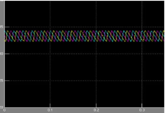
Fig 2: output inductor currents for the circuit the circuit shown in Fig 1. Fig 3:Output voltage across the load for shown in Fig 1.
These are the output inductor current waveforms and we can observe that the currents across every output inductor are sane and all are having same values. So we can say that equal current sharing is achieved by current mode control. And the next figure is about the voltage waveform (exponential in nature) for the circuit shown in Fig 1.
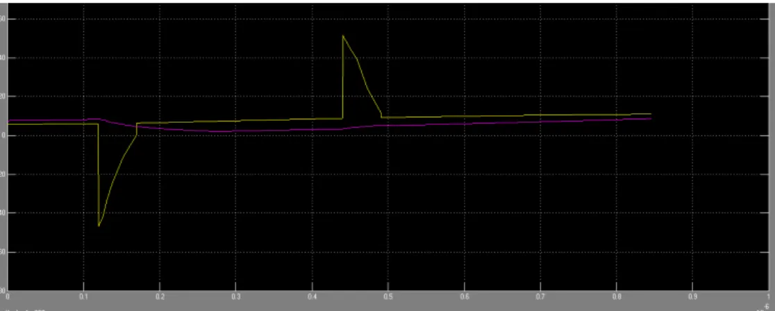
Fig 4: steady state output voltage across the load for Fig 5:steady state output voltage across the the circuit shown in Fig 1(in open loop) without current mode control load for the circuit shown in Fig 1.
current mode control
The above figures are the steady state output voltage waveforms for the circuit shown in Fig 1 without current mode control (Fig 4) and with current mode control (Fig 5). The voltage ripple in open loop is about 4.42 mV whereas in closed loop (with current mode control) is 0.8 mV. So the ripple had been reduced in the case of current mode control.
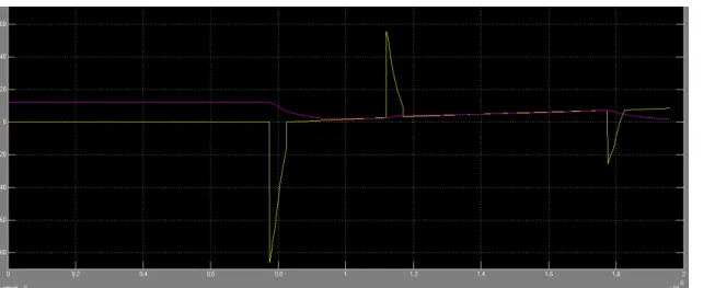
Fig 6: Switching waveforms across the main switch S1(Blue line for voltage, yellow line for current)
Fig 8: Switching waveforms across the main switch S3(Blue line for voltage, yellow line for current)
VI.CONCLUSION
The proposed converter designed has several features and advantages: high output current, high power density, faster switching frequency (1 MHZ) , reduced ripple in the output voltage and by means of current mod e control equal current sharing in each phase is achieved. And as the topology is closed loop, even there are small
disturbances in the input parameters like duty cycle, resonant inductor current and capacitor across the main switches etc., we can get satisfactory results.
VII.REFERENCES
[1] Ashis Mity and Amit Patra, Electrical Engineering, IIT Kharagpur, “Design of a 20 MHz frequency DC-DC buck converter with 84% efficiency for Portable applications”, 2011 24 the annual conference on VLSI design.
[2] Pritam Das, Brial Laan, Seyed Ahmed Mousavi and Gerry moschopolous, 2009, “A non isolated Bi directional ZVS PWM active clamped DC-DC converter, IEEE transactions on Power Electronics, vol24, no 2,pp 553-558.
[3] Gabriel Eirea and Seth R. Sanders “Phase currents unbalance estimation in multiphase buck converters, IEEE transactions on Power Electronics, vol 23, no 1, Jan 2008,pp 137-143.
[4] J.A.A.Quahouq ,L.haung, D. Huard and A.Halberg “Novel current sharing for multi phase converters with digital controller implementation”, Applied Power Electronics conference APEC 2007, Twenty second annual IEEE ,vol 1, pp 148-156.
[5] Y.Jang, M.M.Jovanovic, and Y.Panov “Multi phase buck converters with extended duty cycles” Applied Power Electronics Conference, APEC 2007,Twenty Second Annual IEEE, vol 1,pp 38-44,Feb 2006..
[6] Michel D.Mulligan, Bill Broach and Thomas H.Lee ,” A constant frequency method for improving light load efficiency in synchronous buck converters “,IEEE Power Electronics, letters vol3 ,no 1 march 2005.
[7] Jitendra Agarwal, D.Kastrhe, A.Patra, “An improved control scheme for multi phase buck converter circuits in VRM”, Department of Electrical Engineering, IIT Kharagpur, IEEE PEDS 2005.
[8] Hadja Marecar and Ramesh oruganti senior member, IEEE, “Fast and accurate current sensing in a multiphase buck converters” IEEE PEDS 2005.
[9] Nagaraju H.N.; Patra A; Kastha D: “Design and analysis of four phase synchronous buck converter for VRM applications”,, First India Annual Conference 2004, proceedings of the IEEE INDICON 2004.
[10] W.Haung, G.Schellulian and D.Clavette, “A scalable multiphase buck converter with average current share bus”, IEEE applied Power Electronics conference, APEC 2003.
[11] Peng Xu, Jia Wei ad Fed C.Lee, “Multiphase coupled buck converter, A novel high efficient 12 V voltage regulator module”, IEEE transactions on Power Electronics, vol 18, no 1, January 2003.
[12] Weigu,Weihong QIU, WENKAI WU AMD Issabataarsah “A multiphase Dc/DC converter with hysteretic voltage control and current sharing”, IEEE APEC 2002, pp 670-674.
[13] Sudip K.Mazundaar, Ali H.Nayfeh and Dushan Boroyevich, “ A non linear control scheme for independent stabilization of a parallel Multi phase boost converter by blocking pure zero sequence currents” , IEEE Power Electronics Specialists conference e 2002.
current mode control
[15] N.Jain, P.Jain and G.Jobs,, “Analysis of a zero voltage transition Boost converter using a soft switching auxiliary circuit with reduced conduction losses “ in proceedings of the 32 nd IEEE annual Power Electronics specialists conference(PESC 01) vol 4,pp 1799-1804,,Vancouver, Canada 2001.
[16] X.W.Zhou, P.Wog, F.C.Lee and A.Q.Huang, “Investigation of candidate VRM topologies for future microprocessors”, IEEE transactions on Power Electronics, Nov 2000,pp 1172-1182.
[17] Chin Chang, “Robust Control of DC-DC converters: Buck converter”, Power Electronics Specialists conference, 1995, 26 th annual IEEE volume 2