Study of Commutation Regime for Phase Shift Series
Resonant Inverters
TOMȘE Marin T., GORDAN Cornelia E.
University of Oradea, Romania,
Department of Electronics, Telecommunications and Information Technologies Faculty of Electrical Engineering and Information Technology
410087, Str. Universității No 1 Oradea, Bihor, Romania, E-Mail: mtomse@uoradea.ro
Abstract – Some typical applications of series resonant inverters refers to the development of power supplies for the inductive heating field. Phase shift method is of a great interest for the command of the above mentioned inverters. Concerning this command method, in the paper was developed a detailed study to determine the conditions under which the power switches commutation takes place at zero voltage (Zero Voltage Switching) (ZVS). The authors studied two different ways for the power switches command signals dephasing. For every situation were etablished the power switches having trouble switching. Also, were identified the parameters that influence the power switches commutation regime Based on ORCAD simulations were obtained the limit values of these parameters, values that delimit the non-ZVS commutation regime from the ZVS regime.
Keywords: series resonant inverter; phase shift; ZVS.
I. INTRODUCTION
The development of power semiconductor devices easily to command, working at high frequencies and having high capacity in current and voltage, allowed capitalization of series resonant inverters advantages. In this context these inverters disadvantages are reduced [1], [2], [6].
There are several methods for series resonant inverters command, namely: frequency command, PWM command, phase shift, impulses density modulation command and so on. But for the inductive heating field, the authors consider that the best method is phase shift. This command method allow the power switches switching in ZVS regime and provide the output power control, while maintaining a near unity power factor [2] [3], [4].
The paper presents the authors study about establishing the conditions for the power switches switching at zero voltage (ZVS regime).
There are two different ways for the four power switches command signals dephasing, in the inverter bridge. For every dephasing situation exist different switches with switching trouble.
Because of this reason, the study analyses both dephasing modes to determine the differences between them.
II. SERIES RESONANT INVERTERS COMMAND BY PHASE SHIFT METHOD
The block diagram of a power supply for the inductive heating field, using a phase shift command series resonant inverter, is presented in Fig.1. This command method developes the inverter bridge switches command using impulses with a 0,5 filling factor and the switching frequency a little bit bigger than the resonant frequency of the load circuit. The adjustment of the output power is achieved by the relative dephasing of the two command voltages with a angle from the position they have for the maximum output voltage. [5]
Fig.1. Block diagram of series resonant inverter with phase shift command.
III. SERIES RESONANT INVERTER OPERATION IN ZVS REGIME
The analyse is made for the circuit from Fig. 1 using an ORCAD simulated circuit elements model.
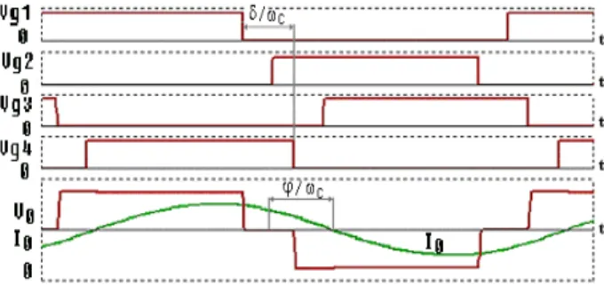
For the power switches were used IGBTs. The waveforms of the parameters describing the inverter’s operation for the first command mode are presented in Fig.2.
Fig. 2. Waveforms of the parameters describing the inverter’s operation (ZVS regime) ( 1 dephasing mode)
It is observed that there are times when the output voltage is zero. This happens when a switch is in conduction and also the diode from the arm in from of the switch is in conduction. In the case of the phase shift command sequence presented in Fig. 2, the switches direct command is made when the load current circulates through their anti-parallel diodes. As a result, the switches direct commutation is with minimal loss.
Switches inverse commutation develops for a different from zero current. For this reason it is required to place a capacitive snuber in parallel with every switch, to ensure a coomutation at a zero voltage (ZVS) with minimal loss.
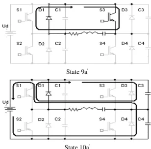
If considering the inverter functioning based on the obtained waveforms one finds that inverter has ten different states during a commutation period, as is presented in Fig. 3.
Fig. 3. Resonant inverter commutation states for ZVS regime (mode 1)
The inverter power circuit configurations corresponding to the above commutation states, for the ZVS regime commutation case, are presented in Fig. 4. Even if the commutation frequency is bigger than the load circuit resonace frequency, ZVS regime can be lost if there is not enough time to download the snubber capacitors placed in parallel with the power switchers. These capacitors exist even if they are not connected
externally, ecause of the power switchers parasitic capacities.
State 1a
State 2a
State 3a
State 4a
State 5a
State 7a
State 8a
State 9a
State 10a
Fig. 4. Power circuit configurations for the series resonant inverter commutation states (ZVS regime) (1 dephasing mode)
As mentioned above, exist two dephasing modes for the case of switches command impulses. So far, was analysed no.1 dephasing mode, for which the command signals for S3 and S4 switches are delayed in comparison with command signals for S1 and S2 switches.
Now will be analysed no.2 dephasing mode, for which the command signals for S1 and S2 switches are delayed in comparison with command signals for S3 and S4 switches. The simulation results obtained for no.2 dephasing mode, with a ZVS regime for the power switches commutation, are presented in Fig. 5
Fig. 5. Waveforms of the parameters describing the inverter’s operation (ZVS regime) ( no.2 dephasing mode)
If analyzes the inverter operation based on the obtained waveforms, account as it has all ten distinct states during a commutation period, as presented in Fig. 6.
Fig. 6. Resonant inverter commutation states for ZVS regime (mode 2)
IV. SERIES RESONANT INVERTER OPERATION IN NON-ZVS REGIME
The obtained waveforms for a commutation regime at a voltage different from zero (non-ZVS) are presented in Fig. 7. Account that D3 and D4 diodes are not in conduction, which means that S3 and S4 switches will be brought in conduction at a voltage different from zero. This happens because C3 and C4 capacitors are not completely unloaded until the switches, they are in parallel position with, will be commanded for being taken in conduction.
Fig. 7. Waveforms of the parameters describing the inverter’s operation (non-ZVS regime) ( no.1 dephasing mode) Analysing the inverter operation for the case of non-zero voltage commutation conditions, one can observe that the inverter has all ten distinct states during a commutation period, as presented in Fig. 8.
Fig. 8. Resonant inverter commutation states for non-ZVS regime (mode 1)
Power circuit configurations of the series resonant inverter for the commutation states in the case of non-ZVS regime commutation are presented in Fig. 9.
State 2a
State 3a
State 4a
State 5a
State 6a
State 7a
State 8a
State 9a
State 10a
Fig. 9. Power circuit configurations of the series resonant inverter commutation states (non-ZVS regime) (no.1
dephasing mode)
The resulted waveforms for the non-ZVS commutation regime for no.2 command mode are presented in Fig. 10.
Account that D1 and D2 diodes are not in conduction, which means that S1 and S2 switches will be brought in conduction at a voltage different from zero. This happens because C1 and C2 capacitors are not completely unloaded until the switches, they are in parallel position with, will be commanded for being taken in conduction.
Fig.10. Waveforms of the parameters describing the inverter’s operation (non-ZVS regime) ( no.2 dephasing mode)
Analysing the inverter operation in these conditions, one can observe that it has all ten distinct states during a commutation period, as presented in Fig. 11.
V. DETERMINING FACTORS INFLUENCING THE POWER SWITCHES OPERATION REGIME
To determine the factors influencing the power switches operation regime was developed a big number of simulations, for different values of the command angle (), of the commutation period (Tc) and of the load parameters.
Analysing the simulation results was observed that that the S1 şi S2 power switches always work in ZVS regime, while the S3şi S4 power switches can loose ZVS regime. This observation can be explained as follows: while commuting S1 switch (transition from 10a state to 1a state for ZVS regime and transition from 10a’ state to 1a’state for non-ZVS regime) and S2 switch (transition from 5a state to 6a state for ZVS regime and transition from 5a’state to 6a’state for non-ZVS regime) the load current has an average value allowing timely task the discharging of the capacitors connected in parallel with these switches. This allows diodes to enter the conduction.
The commutation of S3 switch (transition from 6a state to 7a state for ZVS regime and transition from 6a’ state to 7a’state for non-ZVS regime) and S4 switch (transition from 1a state to 2a state for ZVS regime and transition from 1a’state to 2a’ state for non-ZVS regime) takes place when the load current has small values. Because of this reason sometimes the ZVS commutation is lost.
Insisting in particular on the S3 and S4 switches commutation regime of was obtained the conclusion that exist four parameters that establish the commutation regime for a certain command angle: commutation period (Tc), load current amplitude (I0m), the phase difference between load voltage and current () and C3 and C4 capacitors discharge time (td).
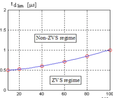
Between ZVS regime and non-ZVS regime exist a limit regime which separates them. This limit regime appears when the snubber capacitor complete discharge takes place shortly before bringing in conduction the corresponding switch. The graphic representation of the four parameters limit values are presented in Fig. 12.
Fig.12. Highlighting measurements characterising the switches commutation regime
The analysed inverter parameters are:
R=0,6 ; L=19,4H; C=880 nF; Q=7,88; Ud=30V; C1 = C2 = C3 = C4 = 2nF.
For different values of the command angle were determined the limit values of the parameters
characterising the power switches commutation regime. Based on the ORCAD simulations were obtained the values presented in TABLE 1. Using a MATLAB linear interpolation relation these limit values represent the bases for the ghraphics presented in Fig. 13.
TABLE 1. Limit values characterising the switches commutation regime
[] 10 20 40 60 80 100
Tc lim [s] 25,83 25,78 25,73 25,58 25,43 25,27
fc lim [Hz] 38710 38790 38870 39100 39320 39510
I0 lim [A] 57,2 53,4 44,3 33,2 20,1 5
lim [] 15 19 27 37 48 61
Fig. 13. Limit values of the parameters characterising the power switches commutation regime
From Fig. 13 can be observed that if the dephasing angle () grows, the commutation frequency must increase in order not to lose the ZVS commutation regime. In these conditions the limit values for load current amplitude (i0) drops, for the dephasing between the load voltage and current () grows and for the snubber capacitor discharging time (td) grows.
Analysing the simulation results for no.2 dephasing mode can be concluded that the S3 and S4 power switches always work in ZVS regime, while S1 and S2 power switches can lose ZVS regime. This observation can be explained because the commutation of S4 switch (transition from 10b state to 1b state for ZVS regime and transition from 10b’ state to 1b’state for non-ZVS regime) and S3 switch (transition from 5b state to 6b state for ZVS regime and transition from 5b’state to 6b’ state for non-ZVS regime) take place when the load current has big values. This load current value can discharge the capacitors connected in parallel positions with the two switchers and allow the diodes to enter the conduction.
The commutation of S2 switch (transition from 6b state to 7b state for ZVS regime and transition from 6b’ state to 7b’state for non-ZVS regime) and S1 switch (transition from 1b state to 2b state for ZVS regime and transition from 1b’state to 2b’state for non-ZVS regime) take place when the load current has small values. Because of this reason sometimes the ZVS commutation is lost.
Comparing the obtained results for the two dephasing modes results that they are very similar. Also, can be observed that the conclusions obtained for no.1 dephasing mode can be transferred to no.2 dephasing mode, if are made the following changing notations:
S1 S4 S2 S3 S3 S2 S4 S1
VI. CONCLUSIONS
In this paper the authors tried to determine the parameters influencing the power switches commutation regime for a series resonant inverter with phase shift command.
Was developed a detailed study concerning the conditions for the case when the power switches commutattions take place for zero voltage (ZVS regime). Were studied two dephasing modes for the four
switches command signals. For this situation was used the ORCAD simulation environment.
Based on the obtained waveforms was concluded that exist ten distinct configurations during a commutation period, both for the ZVS commutation regime and for non-ZVS commutation regime. In the case of non-ZVS regime exist two power switches for which the commutation takes place at a voltage different from zero. In this situation the power loss is big and because of this the switches can overheat and can be destroyed. Also, were identified the parameters influencing the switches commutation regime and based on ORCAD simulations were determined the limit values of these parameters. These limit values separate the non-ZVS commutation regime from the ZVS regime. The resonant inverter commutation regime is characterised by the following four parameters: commutation period (Tc) (or the commutation frequency), load current amplitude (I0m), load voltage and current dephasing () and snubber capacitors discharging time (td).
The general conclusion is that in order to have a ZVS commutation regime for the power switches it is necessary that all indicated parameters to be in „ZVS Regime” area. If any of the parameters is placed in the „non-ZVS Regime” area, two switches commutation take place in non-ZVS regime.
Switches command frequency regulation loop control, in order to ensure the ZVS even in the case when the load parameters are variable, will not be done with a PLL loop. This control will be realised by measuring the load transported by the load current during the ZVS transition
REFERENCES
[1] L. Grajales and F. C. Lee, “Control system design and small signal analysis of a phase-shift-controlled series-resonant inverter for induction heating”, Proc. IEEE Power Electron. Spec. Conf. (PESC 1995), vol. 1, pp. 450–456. [2] P. Viriya, N. Yongyuth, I. Miki, K. Matsuse, “Analysis of
Circuit Operation under ZVS and NON-ZVS Conditions in Phase-Shift Inverter for Induction Heating”, IEEJ Trans. IA, Vol. 126, No. 5, pp.560-567, 2006
[3] M. Tomşe, N. D. Trip, A. Şchiop, C. Gordan,”Modeling and Simulation of a Series Resonant Inverter”, EUROCON 2007, Warsaw, Poland, 2007, pp. 1512-1517.
[4] N. Yongyuth, P. Viriya and K. Matsuse, "Analysis of a Full-Bridge Inverter for Induction Heating Using Asymmetrical Phase-Shift Control under ZVS and NON-ZVS Operation," 7th International Conference on Power Electronics and Drive Systems, Bangkok, 2007, pp. 476-482.
[5] P. Viriya, N. Yongyuth and K. Matsuse, “Analysis of Two Continuous Control Regions of Conventional Phase Shift and Transition Phase Shift for Induction Heating Inverter under ZVS and NON-ZVS Operation,” IEEE Transactions on Power Electronics, Vol. 23, No. 6, pp. 2794-2805, November 2008

![TABLE 1. Limit values characterising the switches commutation regime [] 10 20 40 60 80 100 T c lim [s] 25,83 25,78 25,73 25,58 25,43 25,27 f c lim [Hz] 38710 38790 38870 39100 39320 39510 I 0 lim [A] 57,2 53,4 44,3](https://thumb-eu.123doks.com/thumbv2/123dok_br/18181841.331231/5.892.456.792.247.1138/table-limit-values-characterising-switches-commutation-regime-lim.webp)