VLSI based FFT Processor with Improvement in
Computation Speed and Area Reduction
M.Sheik Mohamed
1, K.Jalal Deen
2, Dr.R.Ganesan
3 1 2Department of Electronics and Instrumentation Engineering, 3 Department of Electronics and Communication Engineering
1 2 3 Sethu Institute of Technology, Anna University, Tamilnadu, India 1 [email protected]
Abstract- In this paper, a modular approach is presented to develop parallel pipelined architectures for the fast Fourier transform (FFT) processor. The new pipelined FFT architecture has the advantage of underutilized hardware based on the complex conjugate of final stage results without increasing the hardware complexity. The operating frequency of the new architecture can be decreased that in turn reduces the power consumption. A comparison of area and computing time are drawn between the new design and the previous architectures. The new structure is synthesized using Xilinx ISE and simulated using ModelSim Starter Edition. The designed FFT algorithm is realized in our processor to reduce the number of complex computations.
Keywords – Radix, FFT, Xilinx, Verilog HDL, Complex conjugate
I.INTRODUCTION
The Fast Fourier Transform (FFT) is commonly used in the field of digital signal processing (DSP) such as filtering, spectral analysis, etc., to compute the discrete Fourier transform (DFT). Using this transform, signals can be moved to the frequency domain where filtering and correlation can be performed with fewer operations. The FFT algorithm should be chosen here to consider the execution speed, hardware complexity, and flexibility and precision [1], [2], [3].
II.FFTARCHITECTURES
This section will review common FFT structures used.
Sequential Processor: The basic sequential processor consists of a processing element (PE) that can compute a butterfly. The same memory can be used to store the data, intermediate results and the twiddle factors. The amount of hardware involved is very small and it takes (N/2) log2N sequential operations to compute the FFT.
Pipeline Processor: To improve the performance of the sequential processor, parallelism can be introduced by using a separate arithmetic unit for each stage of the FFT. This increases the throughput by a factor of log2N when the different units are pipelined. This architecture is also known as cascaded FFT architecture and will be used in our proposed design.
Parallel Iterative Processor: By adding more processing elements to the processor in each sequential pipeline stage, performance can be improved even further. The butterflies can then be computed in parallel in any stage. The total execution time for the parallel iterative processor is log2N cycles. This scheme is used in the FFT processor for radar signal processing.
Array Analyzer: A fully parallel structure can be constructed by having a PE for each of the butterfly operations. This involves a lot of hardware and is not an attractive option for a large N.
multipliers, and adders. Torkelson have classified different pipeline approaches and put into functional blocks with unified terminology [9]. The pipelined architectures can be classified into two types: single-path architectures and multi-path architectures. Several single-path architectures have been proposed: Radix-2 single-path delay feedback, Radix-4 single-path delay feedback, Radix-22 single-path delay feedback, Radix-24 single-path delay feedback, Split-Radix single-path delay feedback, and Split-Radix-4 single-path delay commutator. The multi-path architectures: Split-Radix-2 multi-path delay commutator, Radix-4 multi-path delay commutator, Split-Radix multi-path delay commutator, and Mixed-Radix multi-path delay commutator. The delay feedback architecture is more efficient than the corresponding delay commutator in terms of memory utilization and Radix-2nhas simpler butterfly and higher multiplier utilization [4], [1], [5].
III. FFT Algorithms
Some of the FFT algorithms are discussed as follows.
RADIX-2 Algorithm: The most basic FFT algorithm is the Radix-2 Decimation in Frequency Algorithm. This algorithm decomposes even and odd-indexed frequency samples.
RADIX-4 Algorithm: Decomposing the frequency samples into 2 bins (one each for odd and even samples) gives the Radix-2 Algorithm. Increasing the number of bins to 4 gives the Radix-4 Algorithm.
RADIX-8 Algorithm: Grouping 8 samples together gives the Radix-8 Algorithm.
RADIX-2/4 Algorithm: Split Radix algorithms in general use a separate decomposition for the odd and even samples. For example, the split radix 2/4 Algorithm uses a radix-2 decomposition for the even samples and a radix-4 decomposition for the odd samples. The advantage of this algorithm is that it provides the lowest known number of operations for computing length-2n FFTs. The disadvantage is that the resulting structure is irregular.
RADIX-2/8 Algorithm: Using the Radix-8 decomposition for the odd samples instead of Radix-4 decomposition gives the Split-Radix 2/8 Algorithm.
RADIX-2/4/8 Algorithm: Rearranging 8 samples together in a different manner gives the Radix-2/4/8 Algorithm
III. IMPLEMENTATION
A. Architecture Implemented:
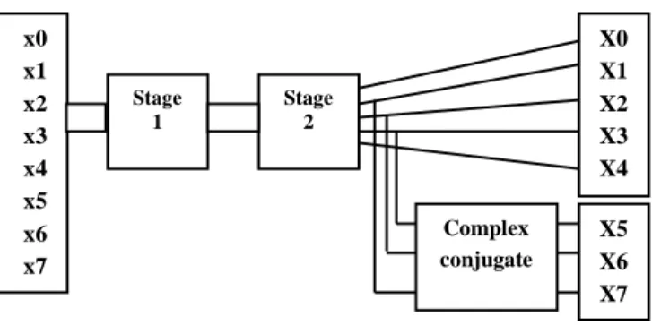
This architecture takes input as x0, x1, x2, x3, x4, x5, x6, x7 and these inputs are given to the first stage of the FFT architecture. Second stage inputs are taken from the first stage and we are getting second stage outputs X0, X1, X2, X3, X4, X5, X6, X7. The system architecture is shown in Fig 1.
Fig. 1 Architecture
The X3’s complex conjugation is X5, X2’s complex conjugation is X6 and X1’s complex conjugation is X7.So this system simplifies the computation and reduce the computation time. Minimization of register is achieved by reducing the computation steps. This system reduces hardware complexity as well as power consumption and can be
reduced up to 37% and 70%. The processor is compared to other implementations based on the area and power consumption. The results expose that our design achieves appropriate reduction in register as well as power.
In order to get the register minimization it is necessary to take conjugate from some of the outputs. This conjugating technique uses a minimum registers comparing to the regular manipulations at the output stage. It reduces the overhead of reordering either the input or the output data. Hence no scrambling is required.
B. Algorithm Implemented
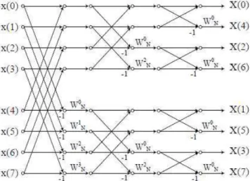
RADIX-2/4/8 Algorithm: Rearranging 8 samples together in a different manner gives the Radix-2/4/8 Algorithm. Mathematically, it is expressed as the signal flow graph for the Radix 2/4/8 algorithm is as shown in Fig 2. Apart from these popular algorithms, researchers have used many other algorithms to build FFT hardware. These include the prime factor algorithm, Winograd algorithm, mixed-radix FFT, algorithms with radix greater than 8 and the Radix24 Algorithm. Specialized algorithms for real-valued data have also been developed.
Our FFT Architecture is based on the Radix-2/4/8 Algorithm and closely resembles the low-power variable-length fast Fourier transform processor by Lin et.al.
Fig. 2 8-pt Radix-2 FFT using Decimation in Frequency Algorithm
C. Software Implemented
VERILOG HDL: It was introduced by Gateway Design Automation in 1984 as a proprietary hardware description and simulation language [6]. VERILOG synthesis tools can create logic-circuit structures directly from VERILOG behavioural descriptions, and target them to a selected technology for realization. Using VERILOG, one can design, simulate, and synthesize anything form a simple combinational circuit to a complete microprocessor system on a chip.
It started out with and still has the following features: [6] 1) Designs may be decomposed hierarchically.
2) Each design element has both a well-defined interface and a precise functional specification.
3) Functional specifications can use either a behavioral algorithm or an actual hardware structure to define initially by an algorithm, to allow design verification of higher level elements that use it; later, the algorithmic definition can be replaced by a preferred hardware structure.
4) Concurrency, timing, and clocking can all be modeled. VERILOG handles asynchronous as well as synchronous sequential-circuit synthesis.
5) The logical operation and timing behavior of a design can be simulated.
file. When one module instantiates another, the compiler finds the other by searching the current workspace, as well as predefined libraries, for a module with the instantiated name. Thus, when using VERILOG-1995, there should be only one definition of each module, usually in a file with the same name as the module. However, VERILOG-2001 actually allows you to define multiple versions ofeach module, and it provides a separate configuration management facility that allows you to specify which one to use for each different instantiation during a particular compilation or synthesis run. This lets you try out different approaches without throwing away or renaming your other efforts. All these features of VERILOG will help better in simulation and synthesis of our proposed architecture.
ModelSimPE: It is an entry-level simulator that offers VHDL, Verilog, or mixed-language simulation. Coupled with the most popular HDL debugging capabilities in the industry, ModelSim PE is known for delivering high performance, ease of use, and outstanding product support. Model Technology’s award-winning Single Kernel Simulation (SKS) technology enables transparent mixing of VHDL and Verilog in one design. ModelSim’s architecture allows platform independent compile with the outstanding performance of native compiled code.
An easy-to-use graphical user interface enables you to quickly identify and debug problems, aided by dynamically updated windows. For example, selecting a design region in the Structure window automatically updates the Source, Signals, Process, and Variables windows. These cross linked ModelSim windows create a powerful easy-to-use debug environment. Once a problem is found, you can edit, recompile, and re-simulate without leaving the simulator. ModelSim PE fully supports the VHDL and Verilog language standards. We can simulate behavioral, RTL, and gate-level code separately or simultaneously. ModelSim PE also supports all ASIC and FPGA libraries, ensuring accurate timing simulations. ModelSim PE provides partial support for VHDL 2008.
The Radix 2/4/8 presented above has been fully coded in Verilog Hardware Description Language. The design is coded in VERILOG, the Xilinx ISE Design Suite 12.1_1 [8] and the ModelSim-Altera 6.5b (Quartus II 9.1) Starter Edition [7] that gives the synthesis and simulation report. The net-list can be downloaded into the FPGA using the same Xilinx tools and Texas Instruments prototyping board. From the architecture of Radix 2/4/8 in Fig 2, the butterfly blocks BF2I and BF2II are described as building blocks in VERILOG code. The FFT is heavily pipelined to achieve as highest clock frequency as possible. Twiddle factors are generated by an external program and embedded to the Verilog code.
D. FPGA Implementation:
The proposed Montgomery multiplier is implemented by using Spartan-3 device xc3s400-4tq144 and is fairly compared with the virtex-5 device 5vlx30ff324-3. The comparison between those two devices has been done based on the parameters like number of slices, number of IO’s, number of bonded IOBs, number of slice flip-flops and time consumption.
Fig. 3 Spartan-3 QFP Package XC3S400-4PQ208C
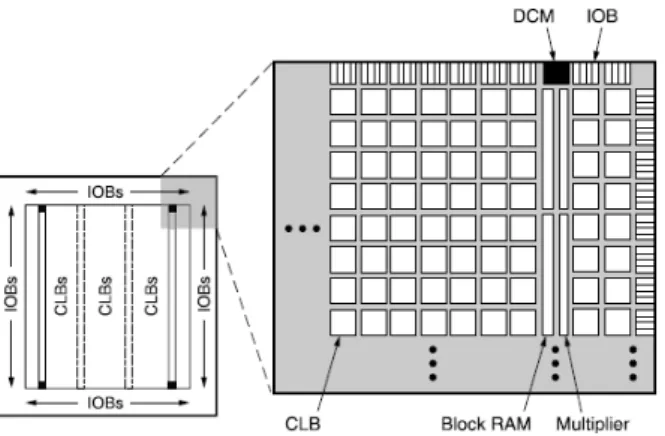
Architetural overview: The Spartan-3 family architecture consists of five fundamental programmable functional elements:
1. Configurable Logic Blocks (CLBs) contain RAM-based Look-Up Tables (LUTs) to implement logic and storage elements that can be used as flip-flops or latches. CLBs can be programmed to perform a wide variety of logical functions as well as to store data.
2. Input/ Output Blocks (IOBs) control the flow of data between the I/O pins and the internal logic of the device. Each IOB supports bidirectional data flow plus 3-state operation. Twenty-six different signal standards, including eight high-performance differential standards are available. Double Data-Rate (DDR) registers are included. The Digitally Controlled Impedance (DCI) feature provides automatic on-chip terminations, simplifying board designs.
3. Block RAM provides data storage in the form of 18-K bit dual-port blocks.
4. Multiplier blocks accept two 18-bit binary numbers as inputs and calculate the product.
5. Digital Clock Manager (DCM) blocks provide self-calibrating, fully digital solutions for distributing, delaying, multiplying, dividing and phase shifting clock signals.
Fig.5 Arrangement of Slices within the CLB
A ring of IOBs surrounds a regular array of CLBs. The XC3S50 has a single column of block RAM embedded in the array. Those devices ranging from the XC3S200 to the XC3S2000 have two columns of block RAM. The XC3S4000 and XC3S5000 devices have four RAM columns. Each column is made up of several 18-Kbit RAM blocks; each block is associated with a dedicated multiplier. The DCMs are positioned at the ends of the outer block RAM columns. The Spartan-3 family features a rich network of traces and switches that interconnect all five functional elements, transmitting signals among them. Each functional element has an associated switch matrix that permits multiple connections to the routing.
The Configurable Logic Blocks (CLBs) constitute the main logic resource for implementing synchronous as well as combinatorial circuits. Each CLB comprises four interconnected slices as shown in Fig.5. These slices are grouped in pairs. Each pair is organized as a column with an independent carry chain. The nomenclature that the FPGA Editor — part of the Xilinx development software — uses to designate slices is as follows: The letter ‘X’ followed by a number identifies columns of slices. The ‘X’ number counts up in sequence from the left side of the die to the right. The letter ‘Y’ followed by a number identifies the position of each slice in a pair as well as indicating the CLB row. The ‘Y’ number counts slices starting from the bottom of the die according to the sequence: 0, 1, 0, 1 (the first CLB row); 2, 3, 2, 3 (the second CLB row); etc. Fig. 5 shows the CLB located in the lower left-hand corner of the die. Slices X0Y0 and X0Y1 make up the column-pair on the left where as slices X1Y0 and X1Y1 make up the column-pair on the right. For each CLB, the term “left-hand” (or SLICEM) indicates the pair of slices labeled with an even ‘X’ number, such as X0, and the term “right-hand” (or SLICEL) designates the pair of slices with an odd ‘X’ number, e.g., X1.
VI. SIMULATION AND RESULTS
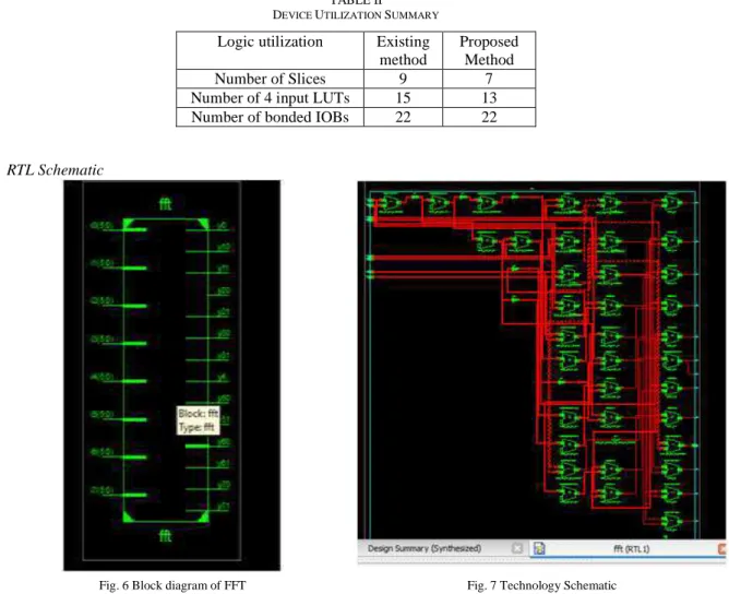
The FFT processor was described with hardware description language Verilog and synthesized with XST tool in Xilinx ISE Design Suite 12.1_1 on Xilinx XC3S400-4PQ208C FPGA chip, the high-performance signal processing applications chip with advanced serial connectivity, and simulated using ModelSim-Altera 6.5b (Quartus II 9.1) Starter Edition. The top-level design shown in Fig. 6, the Xn is input data (8-bit real and 8-bit imaginary), Xk output data (8-bit real and 8-bit imaginary), synchronous reset; rst, clock, chip enable, start, busy, and finish. The synthesis tool has allocated the following resources: 7 slice registers, 13 lookup table and 22 bonded IOs.
The results of the synthesis tool and the timing analysis using the ModelSim simulator indicate a maximum operating frequency of 40 MHz; this provides an execution time of 8 points transform in 249μS.
The implementation results after implementing in Xilinx ISE Design Suite 12.1_1 [8] are listed in Table II. Table II shows the implementation results
TABLE II DEVICE UTILIZATION SUMMARY
Logic utilization Existing method
Proposed Method
Number of Slices 9 7
Number of 4 input LUTs 15 13
Number of bonded IOBs 22 22
A. RTL Schematic
Fig. 6 Block diagram of FFT Fig. 7 Technology Schematic
After performing the synthesize process, the RTL schematic and technology schematic have been created automatically based on the functionality. These schematics are shown in Fig. 6 and 7. The routing between the different cells can be viewed clearly by these schematic.
IV. PERFORMANCE ANALYSIS
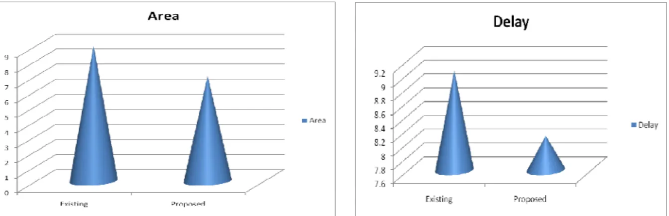
Fig. 8.1.Area comparison (Spartan-3 processor) Fig 8.2 Delay comparison (Spartan3 processor)
V.CONCLUSION
This FFT processor architecture optimized for speed of computation and area reduction has been designed. The algorithm used was a modified version of the DIF-FFT with the inputs and the outputs in natural order (not in bit reversed order). This design eliminates the need of scrambling the inputs and outputs. Although the processor designed is quite small and fast there are some improvements that can be made. Most of the cells used to build the FFT processor have been optimized for speed, area and power consumption. Implementing this technique of taking complex conjugate from some of the outputs recommended for higher point FFTs.
The power consumption can be reduced up to 70%.
REFERENCES
[1] Cortés, I. Vélez, I. Zalbide, A. Irizar, and J. F. Sevillano, “An FFT Core for DVB-T/DVB-H Receivers,” VLSI Design, vol. 2008, Article ID 610420, 9-pages , 2008.
[2] Jesús García1, Juan A. Michell, Gustavo Ruiz, and Angel M. Burón, "FPGA realization of a Split Radix FFT processor," Proc. of SPIE.
Microtechnologies for the New Millennium, vol. 6590, 2007, pp. 65900P-1 to 65900P-11.
[3] Ioan Jivet, Alin Brindusescu, and Ivan Bogdanov “Image Contrast Enhancement using Morphological Decomposition by Reconstruction,”
WSEAS transactions on circuits and systems, Volume 7, Issue 8, August 2008, pp.822-831 Available: www.wseas.us/elibrary/transactions/circuits/2008/27-1425.pdf
[4] L. Yang, K. Zhang, H. Liu, J. Huang, and S. Huang, "An Efficient Locally Pipelined FFT Processor," IEEE transactions on circuits and
systems—II: Express Briefs, VOL. 53, NO. 7, JULY 2006, pp. 585-589.
[5] Jervis, W. B. and E. C. Ifeachor, “Digital Signal Processing: A Practical Approach”, Addison-Wesley Publishing Company Inc., 1993, ISBN 0-201-54413-X
[6] John F. Wakerly, Digital Design Principles and Practices, Fourth Edition, Pearson Education, Inc. 2006. [7] Modelsim manual. Mentor Graphics Corporation. http://support.xilinx.com.
[8] Xilinx, Inc. http://www.xilinx.com/.
[9] S. He and M. Torkelson, “A new approach to pipeline FFT processor,” in Proc. 10th Int. Parallel Processing Symp., 1996, pp. 766–770. [10] Ayinala and K.K.Parhi, “Parallel -Pipelined radix-22 FFT architecture for real valued signals”, in Proc. Asilomar Conf. Signals, Syst.
Comput., 2010, pp. 1274-1278
[11] Ramkumar.B., Kittur,H.M., “Low-Power and Area-Efficient Carry Select Adder” IEEE Trans. VLSI, Issue:99, Publication Year: 2011. [12] Ediz Çetin, Richard C. S. Morling and Izzet Kale, “An Integrated 256-point Complex FFT Processor for Real-time Spectrum Analysis and
Measurement”, IEEE Proceedings of Instrumentation and Measurement Technology Conference, vol. 1, pp. 96-101,Ottawa, Canada, May 19-21, 1997
[13] M. Ayinala and K. K. Parhi, “Parallel-Pipelined radix- FFT architecture for real valued signals,” in Proc. Asilomar Conf. Signals, Syst.
Comput., 2010, pp. 1274–1278.
[14] A.V. Oppenheim, R.W. Schafer, and J.R.Buck, “Discrete-Time Singal Processing”, 2nd ed. Englewood Cliffs, NJ: Prentice-Hall, 1998. [15] H. Wold and A. M. Despain, “Pipeline and parallel-pipeline FFT processors for VLSI implementation,” IEEE Trans. Comput., vol. C-33,
[16] Manohar Ayinala, Michael Brown, Keshab K. Parhi, “Pipelined Parallel FFT Architectures via Folding Transformation” IEEE Trans. on
very Large Scale Integration (VLSI) Systems, vol. 20, no. 6, June 2012.
[17] Y. W. Lin, H. Y. Liu, and C. Y. Lee, “A 1-GS/s FFT/IFFT processor for UWB applications,” IEEE J. Solid-State Circuits, vol. 40, no. 8, pp. 1726–1735, Aug. 2005.
[18] J. Lee, H. Lee, S. I. Cho, and S. S. Choi, “A High-Speed two parallel radix- FFT/IFFT processor for MB-OFDM UWB systems,” in Proc.
IEEE Int. Symp. Circuits Syst., 2006, pp. 4719–4722.
[19] J. Palmer and B. Nelson, “A parallel FFT architecture for FPGAs,” Lecture Notes Comput. Sci., vol. 3203, pp. 948–953, 2004.
[20] M. Shin and H. Lee, “A high-speed four parallel radix- FFT/IFFT processor for UWB applications,” in Proc. IEEE ISCAS, 2008, pp. 960– 963.
[21] M. Garrido, “Efficient hardware architectures for the computation of the FFT and other related signal processing algorithms in real time,”
Ph.D. dissertation, Dept. Signal, Syst., Radiocommun., Univ. Politecnica Madrid, Madrid, Spain, 2009.
[22] K. K. Parhi, “Calculation of minimum number of registers in arbitrary life time chart,” IEEE Trans. Circuits Syst. II, Exp. Briefs, vol. 41, no. 6, pp. 434–436, Jun. 1995.