OPTIMIZATION OF SUPERLATTICES WITH
CENTRAL QUANTUM WELL AND
LUIS EDUARDO PEDRAZA CABALLERO
OPTIMIZATION OF SUPERLATTICES WITH
CENTRAL QUANTUM WELL AND
ALL-OPTICAL LOGIC GATES
Dissertação apresentada ao Programa de Pós-Graduação em Ciência da Computação do Instituto de Ciências Exatas da Univer-sidade Federal de Minas Gerais como re-quisito parcial para a obtenção do grau de Mestre em Ciência da Computação.
Orientador: Omar Paranaiba Vilela Neto
Belo Horizonte
LUIS EDUARDO PEDRAZA CABALLERO
OPTIMIZATION OF SUPERLATTICES WITH
CENTRAL QUANTUM WELL AND
ALL-OPTICAL LOGIC GATES
Dissertation presented to the Graduate Program in Computer Science of the Uni-versidade Federal de Minas Gerais in par-tial fulfillment of the requirements for the degree of Master in Computer Science.
Advisor: Omar Paranaiba Vilela Neto
Belo Horizonte
c
2016, Luis Eduardo Pedraza Caballero. Todos os direitos reservados.
Pedraza Caballero, Luis Eduardo
P371o Optimization of superlattices with central quantum well and all-optical logic gates / Luis Eduardo Pedraza Caballero. — Belo Horizonte, 2016
xxiv, 81 f. : il. ; 29cm
Dissertação (mestrado) — Universidade Federal de Minas Gerais- Departamento de Ciência da
Computação.
Orientador: Omar Paranaiba Vilela Neto
1. Computação - Tesses. 2. Arquitetura de computadores - Teses. 3. Nanofotônica - Teses. 4. Computação evolucionária - Teses. I. Orientador. II. Título.
To the people that believed that this was possible.
Acknowledgments
To my family: Maria, Euclides, Leguis, Andres, Marian and Manuel for their support. To my advisor: Omar Paranaiba, for giving me the opportunity to come from afar to achieve this step in my life. For his teachings, sincerity, critical view and friendship. To my Brazilian brothers: Artur, Andre, Leandro, Thiago, Rafael, Clebson, Gabriel, Keiller, also called: Mitos do Cabral, for their sincere friendship.
To the people that are far away, but it seems they are here: Edinson, Jesus, Jorge, Julio, Johnathan, Virgilio.
To my professors Sonia and Darwin.
To my colleagues: Vinicius, Osvaldo, Alloma, Braulio, Iago.
To the Colombians in BH: Juan, Ricardo, Sergio, Andres, Diego, Jesus, Camilo, Lenka, Carolina, Adriana, Susana.
To Paulo Sergio, Juan Pablo and Marcello for their physical support to develop this work.
To my labmates: Jefferson, Luiz, Fernando, Bruno, Charles, Vitor, Lucas. To the Brazilian government, particularly the CNPQ for the financial support. Finally, to the people of the DCC.
“Three things you can’t take back: a spent arrow, a spoken word and a lost opportunity.”
(Arab proverb)
Resumo
Neste trabalho, dois estudos de casos que relacionam Ciências da Computação e otecnologia são objeto de estudo, a través de duas recentes áreas de pesquisa: Nan-otecnologia Computacional e Nanocomputação.
No primeiro caso, um algoritmo genético (GA) é utilizado para otimizar um tipo de estruturas conhecidas como superredes com poço quântico central. A otimização dessas estruturas é realizada variando a geometria que a compoe, com o intuito de encontrar sistemas que em sua configuração energética, os estados discretos de ener-gia estejam o mais próximo possível do inicio das minibandas. Isto, dado o fato de que estruturas com essas particularidades apresentam alta capacidade de detecção e fotodetetores mais eficientes podem ser desenvolvidos. A variação geométrica consiste em modificar: o número de poços; largura do poço central, dos poços da superrede e das barreiras e altura das barreiras, o que gera inumeráveis configurações energéticas que são difíceis de prever. Desta forma, o processo de otimização se torna um dominio desconhecido, complexo e que demanda um amplo conhecimento de especialistas, por tanto, técnicas de otimização como os GAs são alternativas eficazes que podem auxiliar na solução deste tipo de problemas.
Os resultados obtidos mostram que o GA aplicado neste trabalho é uma tecnica adequada que se adaptou corretamente para o processo de otimização e as melhores estruturas descobertas apresentam características interessantes e grande potencial para serem sintetizadas experimentalmente.
No segundo caso de estudo, os cristais fotônicos são estudados para desenhar e projetar portas lógicas inteiramente óticas, visando o desenvolvimento de uma ger-ação de computadores que opere com alta velocidade de procesamento de dados, baixo consumo energético e baixa dissipação de calor. Isto, motivado pelo fato de que os tran-sistores baseados na tecnologia CMOS estão próximos do seu limite físico de miniatur-ização, além de que os dispositivos computacionais atuais, tem alto consumo energético e alta dissipação de energia em forma de calor.
Neste trabalho são utilizados as guias de onda em cristais fotônicos para contolar
o fenômeno de interferência de luz e desta forma projetar portas lógicas. Duas novas portas lógicas inteiramente óticas utilizando cristais fotônicos foram projetadas, a porta da Maioria e a porta de Feyman. A primeira é muito importante para o desenvolvimento de circuitos otimizados e simplificados, a segunda é uma porta reversível que permite a criação de circuitos no limite mínimo de consumo energético. Adicionalmente, foi aplicada uma metodologia para analisar a robustez destes dispositivos com o objetivo de avaliar a tolerância às falhas ante possíveis erros no processo de crescimento físico. Os resultados obtidos mostram que os dispositivos projetados com essa abordagem são robustos e têm a capacidade de suportar grandes erros no processo de síntese com 95% de confiança.
Palavras-chave: Nanodispositivos Semicondutores, Superredes com Poço Quântico Central, Algoritmo Genético, Cristais Fotônicos, Portas Logicas Fotônicas, Análise de Robustez..
Abstract
In this work, two study cases linking Computer Science and Nanotechnology are stud-ied, through two recent research areas: Computational Nanotechnology and Nanocom-puting.
In the first case, a genetic algorithm (GA) is applied to optimize one type of structures known as superlattices with central quantum well. The optimization of these structures is accomplished varying the geometry that compose it, aiming to find systems in that their energetic configuration, the discrete energy levels must close of the beginning of the minibands. This, due to the that structures with these fea-tures exhibit high capacity detection and efficient photodetectors can be development. The geometrical variation consist in modify: the number of quantum wells; width of the central well, wells of the supperlattice and the barriers and hight of the barriers, generating countless energetic configurations difficult to predict. Consequently, the optimization process becomes a unknown domain, complex and demanding extensive knowledge and intuition of experts, then, optimization techniques such as GAs are effective alternatives to aid in the solution of these problems.
The results obtained here show that the GA is an adequate techniques for the optimization of this kind of structures and the better structures discovery present interesting features and great potential to be synthesized experimentally.
In the second study case, photonic crystals are studied to design and project all-optical logic gates, aiming the development of a computers generation operating with high data processing speed, low power consumption and low dissipation of energy. This, motivated by the reason that the transistor based on CMOS technology is close to its physical limit of miniaturization as a result of various effects that are not found at larger scales, such as current leakage. Also, the computational devices today have high power consumption and dissipation of energy to heat.
In this project, photonic crystals waveguides are used to control the light beam interference effect focusing in the design of all-optical logic gates. Two new logic devices in photonic crystals were proposed in this work, the Majority and Feynman gates. The
former is very important to develop simplified and optimized circuits, the latter is a reversible logic gate that allows the creation of computational circuits in the minimum limit of energy consumption. Additionally, a methodology to analyse the robustness of these devices is applied with the goal to evaluate the fault tolerance in the physical growth. The results obtained show that the devices projected with this approach are robust and have the capacity to tolerate high disorders in the physical growth process with 95 % of confidence level.
Palavras-chave: Semiconductors nanodevices, Superlattices With Central Quantum Well, Genetic Algorithm, Photonic Crystals, Photonic Logic Gates, Robustness Anal-ysis.
List of Figures
2.1 Insulator and conductor energy-band configuration . . . 8
2.2 Semiconductor energy-band configuration . . . 9
2.3 Quantum well structure . . . 9
2.4 Superlattice of quantum wells structure . . . 10
2.5 Two dimensional photonic crystal . . . 11
2.6 Photonic crystal Cavity. . . 12
2.7 Photonic crystal waveguide . . . 12
3.1 AND logic gate proposed by Rani et al. . . 17
3.2 AND logic gate proposed by Yang et al. . . 18
3.3 OR and XOR logic gates proposed by Fu. et al. . . 18
3.4 OR and AND logic gates proposed by Younis et al. . . 19
3.5 Logic device proposed by Goudarzi et al. . . 19
4.1 Superlattice of quantum wells geometry. . . 22
4.2 Energy-band configuration desired. . . 22
4.3 Superlattice of quantum wells structure example. . . 23
4.4 Transmission of superlattice of quantum wells structure example. . . 23
4.5 Localization of the wave function. . . 24
4.6 Simulation result of superlattice example. . . 25
4.7 Chromosome representation . . . 26
4.8 Genetic algorithm evolution. . . 29
4.9 Energy-band localization of the best individual. . . 30
4.10 Energy-band localization of the worst individual. . . 31
5.1 Majority gate simulation results . . . 35
5.2 Feynman gate simulation results . . . 37
5.3 Gaussian distribution. . . 39
5.4 Robustness Analysis test. . . 40
5.5 Lines analysed for the OR device. . . 41
5.6 Regions analysed for the OR device. . . 42
5.7 Regions effect for the OR device. . . 44
5.8 Lines analysed for the XOR device. . . 44
5.9 Regions analysed for the XOR device. . . 47
5.10 Regions effect for the XOR device. . . 49
5.11 Lines analysed for the Majority logic device. . . 49
5.12 Regions analysed for the Majority logic device. . . 52
5.13 Regions effect for the Majority device. . . 54
5.14 Lines analysed for the Feynman logic device. . . 54
5.15 Regions analysed for the Feynman logic device. . . 56
5.16 Regions effect for the Feynman device. . . 59
B.1 Init page of SPQW online Simulator. . . 69
B.2 Simulator module of the SPQW online simulator. . . 70
B.3 Projects module of the SPQW online simulator. . . 71
C.1 Superlattice of quantum wells structure 3. . . 76
C.2 Superlattice of quantum wells structure 4. . . 77
C.3 Superlattice of quantum wells structure 5. . . 78
C.4 Superlattice of quantum wells structure 6. . . 79
C.5 Superlattice of quantum wells structure 7. . . 80
C.6 Superlattice of quantum wells structure 8. . . 81
List of Tables
4.1 Parameters of superlattice of quantum wells structure. . . 22
4.2 Fitness calculation example. . . 25
4.3 Individual parameters and their boundary conditions. . . 26
4.4 Genetic algorithm parameters . . . 28
4.5 Experiment results. . . 29
4.6 Parameters of the best individual found. . . 30
4.7 Simulation result of the best individual found. . . 30
4.8 Parameters of the worst individual found. . . 31
4.9 Simulation result of the worst individual found. . . 31
5.1 Majority gate truth table. . . 34
5.2 Transmission results for all-optical majority gate . . . 36
5.3 Feynman gate truth table. . . 37
5.4 Transmission results for all-optical Feynman gate . . . 38
5.5 Simulations results for the modifications of the all cylinder and the first three lines for the OR device. Std is the standard deviation and CI the confidence interval. . . 41
5.6 Simulations results of the first line regions for the OR device. Std is the standard deviation and CI the confidence interval. . . 43
5.7 Simulation results for the modifications of all cylinders and the first three lines for the XOR device and (0,1) and (1,0) input cases. Std is the standard deviation and CI the confidence interval. . . 45
5.8 Simulation results for the modifications of all cylinders and the first three lines for the XOR device and (1,1) input case. Std is the standard deviation and CI the confidence interval. . . 46
5.9 Simulations results of the first line regions for the XOR device. Std is the standard deviation and CI the confidence interval. . . 48
5.10 Simulation results for the modifications of all cylinders and the first three lines for the Majority device and (0,1,0) and (0,1,1) input cases. Std is the standard deviation and CI the confidence interval. . . 50 5.11 Simulation results for the modifications of all cylinders and the first three
lines for the Majority device and (1,0,1) and (1,1,1) input cases. Std is the standard deviation and CI the confidence interval. . . 51 5.12 Simulations results of the first line regions for the Majority device. Std is
the standard deviation and CI the confidence interval. . . 53 5.13 Simulation results for the modifications of all cylinders and the first three
lines for the Feynman device and (0,1) input case. Std is the standard deviation and CI the confidence interval. . . 55 5.14 Simulation results for the modifications of all cylinders and the first three
lines for the Feynman device and (1,0) input case. Std is the standard deviation and CI the confidence interval. . . 56 5.15 Simulation results for the modifications of all cylinders and the first three
lines for the Feynman device and (1,1) input case. Std is the standard deviation and CI the confidence interval. . . 57 5.16 Simulation results of the first line regions for the Feynman device. Std is
the standard deviation and CI the confidence interval. . . 58
C.1 Parameter of superlattice of quantum wells structure 1. . . 73 C.2 Energy localization of structure 1. . . 73 C.3 Parameter of superlattice of quantum wells structure 2. . . 74 C.4 Energy localization of structure 2. . . 74 C.5 Parameter of superlattice of quantum wells structure 3. . . 75 C.6 Energy localization of structure 3. . . 75 C.7 Parameter of superlattice of quantum wells structure 4. . . 76 C.8 Energy localization of structure 4. . . 76 C.9 Parameter of superlattice of quantum wells structure 5. . . 77 C.10 Energy localization of structure 5. . . 77 C.11 Parameter of superlattice of quantum wells structure 6. . . 78 C.12 Energy localization of structure 6. . . 78 C.13 Parameter of superlattice of quantum wells structure 7. . . 79 C.14 Energy localization of structure 7. . . 79 C.15 Parameter of superlattice of quantum wells structure 8. . . 80 C.16 Energy localization of structure 8. . . 80
Contents
Acknowledgments xi
Resumo xv
Abstract xvii
List of Figures xix
List of Tables xxi
1 Introduction 3
1.1 Motivation . . . 3 1.2 Goals . . . 4 1.3 Contributions . . . 5 1.4 Roadmap . . . 5
2 Background 7
2.1 Semiconductors . . . 7 2.2 Superlattice of Quantum Wells . . . 9 2.3 Photonic Crystals . . . 11 2.4 Genetic Algorithm . . . 12
3 Related Work 15
3.1 Semiconductor Nanodevices Optimization . . . 15 3.2 All-Optical Logic Gates . . . 17
4 Optimization of Superlattices With Central Quantum Well 21
4.1 Problem Definition . . . 21 4.1.1 Superlattice With Central Quantum Well Structures Desired . . 21 4.1.2 Detection of Energy States . . . 22
4.2 Optimization Model . . . 25 4.3 Simulation Results . . . 28
5 Logic Devices with Photonic Crystals 33
5.1 Majority and Feynman Gates . . . 33 5.1.1 Majority Gate . . . 34 5.1.2 Feynman Gate . . . 36 5.2 Robustness Analysis of All-Optical Logic Gates . . . 38 5.2.1 OR Gate . . . 40 5.2.2 XOR Gate . . . 44 5.2.3 Majority Gate . . . 48 5.2.4 Feynman Gate . . . 53 5.3 Cascading of Logic Gates . . . 58
6 Conclusions and Future Work 61
6.1 Future Work . . . 62
Bibliography 63
Appendix A Publications 67
A.1 Published . . . 67 A.2 In Production . . . 67
Appendix B SPQW Online Simulator 69
Appendix C Superlattices of Quantum Wells Structures 73
List of Acronyms
Acronym Description
CQW Central Quantum Well
GA Genetic Algorithm
Phc Photonic Crystal
SPQW Superlattice of Quantum Wells
Chapter 1
Introduction
1.1
Motivation
In recent years, two research areas that link computer science and nanotechnology have been gaining ground. These are: computational nanotechnology and nanocomputing.
The first focusses on the application of computational tools and algorithms to support the evolution of the nanoscience and nanotechnology, specifically to develop and discover new materials and devices at the nano scale. On the other hand, nanocom-puting investigates materials and devices at nano scale as alternatives technologies to develop new generations of computers with low power consumption and high data processing speed.
In this work, two study cases related with computational nanotechnology and nanocomputing are investigated.
The first motivated by the difficulty found by scientists to optimize one kind of quantum structures known as superlattices with central quantum well (SPQW). These are periodic structures formed by the repetition of quantum wells with thin barriers separating them and a quantum central well. Consequently, discrete energy states and minibands are present in their energy-band configuration. Modifications in the geometry of it, such as: number of quantum wells, width of quantum wells and barriers, height of the barriers, cause different energy-band configurations.
The localization of the discrete energy states and minibands in SPQW is accom-plished through a visual observation by an expert, demanding extensive knowledge and intuition. In addition, finding structures with specific energy-band configuration is a hard, empirical and slow optimization process.
For this reason, the use of robust, effective and efficient computational techniques and optimization algorithms to support this process is necessary. Thus, a genetic
4 Chapter 1. Introduction
gorithm is an adequate optimization approach to find SPQW structures with desired energy-band configuration in order to develop new optoelectronic devices such as pho-todetectors.
The second study case is inspired by the reason that the silicon transistor is close to its physical limit of miniaturization as a result of various effects that are not found at larger scales, such as current leakage. Consequently, smaller computers with greater data processing speed and high capacity of data storage might not be developed. Also, the computational devices today have high power consumption and dissipation of energy to heat. Then, it is necessary to explore new materials and technologies to find the successor of silicon transistor.
One possible alternative is the optical technology. In this, the information pro-cessing is realized using all-optical devices. For optical technology is expected consider-able reduction of dissipation, low power consumption and high speed of data processing. In this way, photonic crystals are materials with low absorption and periodic refractive indices. The periodicity can be in one, two or three dimensions. Two di-mensional photonic crystals can be designed to create a complete photonic band gap, preventing light from propagating in certain directions with specified frequencies. This phenomena is used to create a photonic crystal waveguide. A waveguide is a con-trolled defect in the crystal, able to guide the light in desired directions of propagation, Joannopoulos et al. [2008]. Then, a photonic crystal waveguide is a perfect platform to design all-optical logic devices aiming the creation of photonic integrated circuits.
1.2
Goals
For the superlattice with central quantum well optimization, the goal is to find struc-tures with a desired energy-band configuration through a genetic algorithm by varying the geometry parameters that compose them. This, aiming to develop and discover new optoelectronic devices such as photodetectors with high detection capacity. The parameters to be modified are: number of quantum wells, width of the central quantum well, width of the quantum wells that form the superlattice, width of the barriers and height of the barriers.
1.3. Contributions 5
low power consumption and high speed of data processing.
1.3
Contributions
The main contributions of this project are: for the superlattices with central quantum well optimization, an approximated method was developed to achieve automatically the energy-band configuration of these structures. This method in conjunction with a genetic algorithm are applied to find superlattices of quantum wells with desired energy states. The best structures found in this work have great potential to be grown experimentally in order to develop optoelectronic devices such as photodetectors.
In the work with photonic crystals, two all-optical logic gates were projected using the light beam interference effect. These are: the Majority and Feynman gates. The first is very important to develop simplified and optimized circuits, the second is a reversible logic gate that allows the creation of circuits in the minimum limit of energetic consumption. Additionally, a robustness analysis methodology was proposed and demonstrated that the all-optical logic devices designed with photonic crystals waveguide are robust and can tolerate high errors in the growth physical process.
1.4
Roadmap
Chapter 2
Background
Nanocomputing and Computational Nanotechnology are two recent research areas link-ing Computer Science and Nanotechnology, so, in order to better understand this work, this section gives an introduction to what Semiconductors, Superlattices of Quantum Wells Structures, Photonic Crystals and Genetic Algorithms are, and how they work.
2.1
Semiconductors
In solid state physics, crystals are defined as periodic arrangements of atoms or molecules characterized by a crystal lattice, which has the geometrical information of the periodic pattern. Consequently, an atomic crystal determines a periodic poten-tial which produces fascinating consequences in the electron transport throughout the crystal, and characterizes the electric properties of the material, Rezende [2004].
Electrons suffer scattering in crystals when the size of the scatterers (atoms or molecules) are of the order of the De Broglie wavelength, giving rise to interference phenomena between the multiple scattered electron waves. Such interference can be constructive, determining allowed states known as bands, e.g., valence and conduction bands; or destructive, determining forbidden states known as band gaps. Each crystal has its own energy-band configuration. Thus, there are several possible energy-band conditions to consider, Neamen [2003].
First, when the material is an insulator, the last energy band with electrons is completely filled with electrons. Then, if an electric field is applied, there are no particles to move, so there will be no current, as shown in Figure 2.1a, Neamen [2003].
In the second case, the crystal has the characteristics of a conductor, exhibiting a very high electrical conductivity. For this condition, the last energy band with electrons
8 Chapter 2. Background
Eg Fermy Energy Valence Band Conduction Band
-
-
-
- -
-
-
- -
- -
-
(a) Fermy Energy Conduction Band--
-
- -
-- --
--
-
-Valence Band (b)
Figure 2.1: Energy band configuration for (a) Insulator and (b) Conductor
is not completely filled, so an electric field can put electrons in movement, thus, allowing conduction, as illustrated in Figure 2.1b, Neamen [2003].
Finally, when the material is a semiconductor, the last energy band of a crystal is completely filled, only at temperature T = 0 K. When the temperature is higher than zero, valence band electrons can gain enough thermal energy to reach the next band, called conduction band, which was empty atT = 0. The migration of electrons to the conduction band leaves, in the valence band, states that behave such as positive charge carriers, called holes. The electrons in the conduction band and holes in the valence band produce electrical current under the action of an external field. The conductivity of the material depends on the number of electrons that passes into the conduction band, which can be calculated probabilistically. This amount of electrons is proportional to the temperature and the inverse of the energy gap between the two bands. This energy is represented by Eg, where g is the gap index. The materials which are insulators at T = 0 K, but have an Eg relatively small, on the order of 1
eV or less at room temperature, have significant conductivity and, therefore, are called semiconductors. Figure 2.2 shows the occupation of the valence and conduction bands in a semiconductor.
In these materials, the number of electrons in the conduction band can be higher in relation to an insulator, but it is still much less than the number of free electrons in a metal. Therefore, the conductivity of the semiconductor is much smaller than that of metals. The main difference between an insulator and a semiconductor is the value of Eg. For example, silicon has Eg = 1.1 eV and is a semiconductor, while diamond which has the same structure of Silicon (Si), but comprised of atoms of Carbon (C) has Eg = 5 eV, and behaves as a good insulator. The Silicon Oxide, SiO2, has an
2.2. Superlattice of Quantum Wells 9
Eg Fermy Energy Valence Band
Conduction Band
-
-
-
- -
-
-
- -
- -
-
(a)
Eg Fermy Energy Valence Band
Conduction Band
-
- - - - - -
-
-
-
- -
+ + + + + +-
(b)Figure 2.2: Energy band configuration for (a) Semiconductor at T = 0K and (b) Semiconductor at T >0K
conduction band decreases exponentially with the increase of the Eg
kBT ratio, wherekB
is the Boltzmann constant, as described in Rezende [2004].
2.2
Superlattice of Quantum Wells
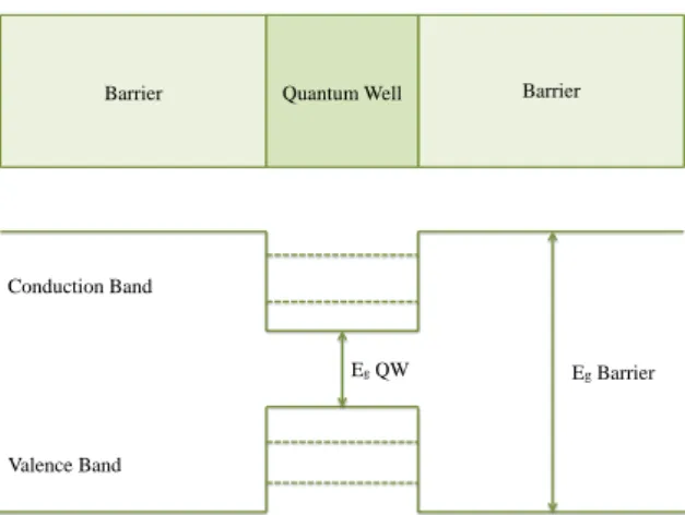
A semiconductor quantum well is a sandwich structure, in which a piece of narrow-gap material (well) is placed between two pieces of wider-gap material (barriers), as shown in Figure 2.3. This is a kind of quantum-confined structure in which the motion of the electrons (and/or holes) are confined in one directions by the potential barriers, Duan and Guojun [2005].
The quantum confinement is provided by the discontinuity in the band gap at the interfaces, which leads to a spatial variation of the conduction and valence bands, as shown in the lower half of the Figure 2.3.
Quantum Well
Barrier Barrier
Conduction Band
Valence Band
Eg QW Eg Barrier
10 Chapter 2. Background
Thus, the motion of the electrons and holes will be quantized in the growth (z) direction, giving rise to a series of discrete energy levels, as indicated by the dashed lines inside the quantum well in Figure 2.3. The motion in the other two directions (i. e. the x-y plane) is still free, and so we have quasi two-dimensional (2-D) behaviour, Kasap and Capper [2007].
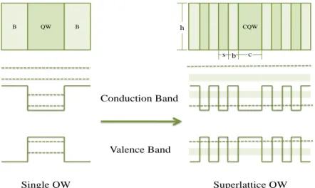
A superlattice of quantum wells structure consists of many repeated quantum wells with thin barriers separating them, as illustrated in Figure 2.4. Superlattices behave like artificial one-dimensional periodic crystals, in which the periodicity is de-signed into the structure by the repetition of the quantum wells. The electronic states of superlattices form delocalised minibands as the wave functions in neighbouring wells couple together through the thin barrier that separates them, Kasap and Capper [2007].
CQW
B QW B
Single QW Superlattice QW Valence Band
Conduction Band
c b s h
Figure 2.4: Superlattice of Quantum Wells Structure. Dashed lines represents discrete energy levels and the shaded areas minibands.
2.3. Photonic Crystals 11
2.3
Photonic Crystals
The optical analogue of an atomic crystal semiconductor is known as a photonic crystal, which is a material whose dielectric function is periodic and they are described by an underlying crystal lattice. As electrons in periodic potential, electromagnetic waves in a photonic crystal undergo scattering when their wavelengths are of the order of the size of the dielectrics forming the crystal, Joannopoulos et al. [2008].
Photonic bands (allowed states) arise as a consequence of constructive interference phenomena, and photonic band gaps arise as a consequence of destructive interference phenomena. Defects in the periodic structure can be introduced in a photonic crystal and they can induce the localization of the electromagnetic field around the defect, and these localized states can have associated frequencies inside the photonic band gap region. Photonic crystals can be periodic in one, two or three dimensions, each of these offering particular functionalities and applications, Joannopoulos et al. [2008].
Two dimensional photonic crystals, as shown in Figure 2.5, can be designed to create a complete photonic band gap, preventing light from propagating in certain directions with specified frequencies (i.e., within a certain range of wavelengths of light colors).
Figure 2.5: Two dimensional photonic crystal. Taken from Joannopoulos et al. [2008].
In particular, there are two types of defects that can be introduced in two-dimensional photonic crystals: point defects and line defects. The former are known as cavities, illustrated in Figure 2.6, and the latter as waveguides, as shown in Figure 2.7.
12 Chapter 2. Background
(a) (b)
Figure 2.6: Photonic Crystal Cavity. (a) Dielectric distribution of the structure and (b) Electric field distribution.
is usually high. In this way, photonic crystals allow optical devices working in the low losses and low energy-consumption regime, Joannopoulos et al. [2008].
(a) (b)
Figure 2.7: Photonic Crystal Waveguide. (a) Dielectric distribution of the structure and (b) Electric field distribution.
Photonic crystals have become very promising systems to achieve the desired all-optical information processing in photonic circuits. In particular, cavities and waveg-uides embedded in photonic materials can be used to design efficient all-optical com-putational devices with flexible functionalities.
2.4
Genetic Algorithm
Computational Intelligence is a branch of Computer Science that uses algorithms and techniques that mimic some cognitive abilities such as recognition, learning and devel-opment, to create programs, somehow intelligent. The best-known and used algorithms are: Genetic Algorithm, Artificial Neural Networks and Fuzzy Logic, Neto [2014].
2.4. Genetic Algorithm 13
which favor the fittest individuals living longer and therefore more likely to reproduce. Typically, the GAs operate as explained in Algorithm 1, Mitchell [1998].
Algorithm 1 Genetic Algorithm
1: procedure GA(F itness, n, p, r, m)
2: F itness: A function that assigns an evaluation score, given a hypothesis.
3: n: The number of generations.
4: p: The number of hypotheses to be included in the population.
5: r: The fraction of the population to be replaced by Crossover at each step.
6: m: The mutation rate.
7: Initialize population: P ← Generate p hypotheses at random.
8: Evaluate: For eachh in P, compute F itness(h).
9: while Stop condition is not satisfied do
10: Create a new generation, Ps:
11: Select: Probabilistically select (1−r)pmembers of P to add to Ps.
12: Crossover: Probabilistically select pair of hypotheses from P. For each pair, (h1, h2) , produce two offspring by applying the
crossover operator. Add all offspring to Ps.
13: Mutate: Choose m percent of the members of P, with uniform probability. For each, invert one randomly selected bit in its representation.
14: Update: P ←Ps.
15: Evaluate: for each h inP, compute F itness(h).
16: speed← computeSpeed(
gpx.track(i).segment(j).delta_s(q), gpx.track(i).segment(j).delta_t(q));
17: end while
18: Return the hypothesis from P that has the best fitness.
19: end procedure
These algorithms are inspired by the genetic processes of biological organisms to search for optimal solutions. To do so, it proceeds as follows: each potential solution to a problem can be encoded in a structure called chromosome, which consists of a string of bits or symbols, Michalewicz [2013]. So these chromosomes represent individuals that are evolved over several generations, similar to living beings, according to the principles of natural selection and survival of the fittest, as described by Darwin [1859]. Simulating these processes, Genetic Algorithms are able to evolve solutions to real world problems.
14 Chapter 2. Background
These new solutions will be evaluated and their skills will determine your probability of staying in subsequent generations, Golberg [1989].
Chapter 3
Related Work
3.1
Semiconductor Nanodevices Optimization
Computational Nanotechnology (or Computational Nanoscience) focuses in the appli-cation and development of algorithms and computational systems to aid the advances of nanoscience and nanotechnology. In this scenario, many computational techniques have been applied to support several studies researching the development and discovery of new materials and devices in the nano-scale.
In a work developed by Singulani et al. [2008] two computational intelligence techniques were applied, namely, Artificial Neural Network (ANN) and Genetic Algo-rithm to the growth of self-assembled quantum dots. The ANN was used to associate the growth input parameters with the mean height of the deposited quantum dots. The six different growth parameters used as input to create the ANN are: the indium flux in the reactor, the growth temperature, the deposition time, the width of the layer on top of which the dots are nucleated, the aluminum and indium contents of this layer material. Once the Neural Network was created, validated and tested, it has combined with the GA, enabling us to obtain the growth parameters which are, in principle, most suitable for minimizing the quantum dot mean height. This is accomplished by using an ANN to infer the behavior of the quantum dots, and after that, the GA technique to obtain the parameters configuration which leads to the minimum quantum dot mean height possible, given the growth parameters ranges used as input to the ANN.
Passaro et al. [2010] present a self-consistent optimization of multi-quantum well based nanostructured semiconductors. Two study cases are evaluated, to known: sym-metric MQW of three wells with a larger one in the middle and MQW of ten wells and electric contacts. A Genetic Algorithm is used for the search module, based on the solution of the coupled Schrödinger and Poisson equation.
16 Chapter 3. Related Work
In another work, Deb et al. [2010] applied Genetic Algorithm (GA) and particle swarm optimization (PSO) techniques to determine the optimized system parameters for modulation doped AlxGa1−xAs/GaAs quantum well nanostructures. Electrical
characteristics of carrier in quantum well are controlled by system parameters like quantum well width, spacer layer thickness, doping concentration, lattice temperature, external dc biasing field and frequency of applied ac field. All these parameters are related in such a way that it is very difficult to predict optimized parameter values for desired electrical characteristics. Optimized parameters computed with both tech-niques are analyzed to predict the flexibility in terms of parameters which may be utilized during the fabrication of better nanodevices. The authors showed that PSO achieved slightly better results.
Cotta et al. [2014] use a genetic algorithm for the the first quantitative study of parameters optimization for semiconductor microcavities synthesis under uncertainty. In this, optimal parameter set (aluminum concentrationsx, thickness and the number of the layers) were found based on the reflectance spectra of aAlxGa1−xAssemiconductor
microcavity. These parameters may offer increased robustness in the growth process, while providing a considerable Quality Factor and the desired position of the cavity resonance.
Also, evolutionary optimization has been used by Feichtner et al. [2012], to find improved nanoantenna structures and Chen et al. [2007] optimized the focusing qual-ity of integrally gated Carbon Nanotube (CNT) field emission devices by numerical methods that include GAs. Ginzburg et al. [2011] presented a method for designing plasmonic particles with desired resonance spectra by exploiting the interaction of lo-cal geometry with surface charge distribution and applying an evolutionary algorithm. Forestiere et al. [2010] used GAs to design metal nanoparticle arrays that produce broadband plasmonic field enhancement over the entire visible spectral range.
3.2. All-Optical Logic Gates 17
3.2
All-Optical Logic Gates
The first step for development of photonic computational circuits is the design and creation of all-optical logic gates. Recently, many schemes have been proposed to realize all-optical logic gates.
Rani et al. [2013] report an AND optical logic gate, shown in Figure 3.1, based on two dimensional triangular lattice of air holes in Si. The design of the structure consists of Y-branch waveguide without nonlinear materials and optical amplifiers. A point defect was inserted in the central rod of the structure to decrease the output power, when one of the inputs is set in 1. When both inputs are 1, the output power was increased so that a high transmission is obtained and an AND gate is accomplished.
Port A Port B
Output Y
Figure 3.1: Schematic structure for AND logic gate proposed by Rani et al. [2013].
In another recent work, Yang et al. [2013] propose an all-optical AND gate based on a two-dimensional photonic crystal, illustrated in Figure 3.2. The device is com-posed of a ring resonator waveguide with two input-port waveguides and one output-port waveguide in triangular-lattice photonic crystals. The logic AND gate proposed can operate at various wavelengths such as 1.30, 1.43, 1.45, 1.49, 1.51, and 1.55 µm, considering the definitions of logic 0 and 1 being less than 35% and more than 95%, respectively.
18 Chapter 3. Related Work
Port A
Port B
Port Y
Figure 3.2: Schematic structure for AND logic gate proposed by Yang et al. [2013].
A
B
C
(a)
A
B
C
(b)
Figure 3.3: Schematic structure for the (a) OR and (b) XOR logic gates proposed by Fu et al. [2013].
Younis et al. [2014] propose two novel designs of compact, linear, and all-optical OR and AND logic gates based on photonic crystal architecture. The proposed devices are formed by the combination of the ring cavities and Y-shape line defect coupler placed between two waveguides. The suggested design for AND gate offers ON to OFF logic level contrast ratio of not less than 6 dB and the suggested design for OR gate offers transmitted power of not less than 0.5. On top of that, the proposed OR and AND logic gates can operate at bit rates of around 0.5 and 0.208 T b/s, respectively. Further, the calculated fabrication tolerances of the suggested devices show that the rods radii of the ring cavities need to be controlled with no more than±10% and±3%
fabrication errors for optical OR and AND gates, respectively. The schematic structure of these all-optical logic gates is shown in the Figure 3.4
3.2. All-Optical Logic Gates 19
(a) (b)
Figure 3.4: Schematic structure for the (a) OR and (b) AND logic gates proposed by Younis et al. [2014].
between the two input beams is π
2, they interfere together constructively or
destruc-tively to realize the logical functions. The authors reported that the device can acts as an XOR and an OR logic gate. The frequency operation range of the device is 0
to 0.45 (a
λ), this ratio was set 0.419 for low dispersion condition, correspondingly the
lambda is equal to1.55µm. The maximum delay time to response to the input signals is about 0.4 ps, hence the speed of the device is about 2.5 T Hz. Also6.767 dB is the maximum contrast ratio of the device.
A
B Q2
Q1
Figure 3.5: Schematic structure proposed by Goudarzi et al. [2016]. The output in Q1 is the XOR function and in Q2 is the OR function.
Chapter 4
Optimization of Superlattices With
Central Quantum Well
This chapter presents the methodology to apply the genetic algorithm, the problem definition, the optimization model and the simulation results of the optimization of the superlattices with central quantum well.
4.1
Problem Definition
4.1.1
Superlattice With Central Quantum Well Structures
Desired
The design and search of superlattices of quantum wells with desired energy-band configuration behaviour is a very difficult process. However, this is an important step for the development and discovery of new optoelectronic devices.
The structures of our interest are geometrically composed by a central quantum well, n quantum wells to the left and right of the CQW and (2∗(n+ 1)) barriers, see Figure 4.1. Modifications in the geometry of the structure produce different energy-band configuration, i.e, variations in the number of quantum wells, the width of the central quantum well, width of the quantum wells forming the superlattice, width and height of the barriers, are responsible for these effects.
The target here is to find structures restricted to the following condition:
The discrete energy levels must be close of the beginning of the minibands in the energy-band configuration of the structure, as illustrated in the Figure 4.2a. The main reason is that when an electric field is applied on the structure, the discrete energy level comes into the miniband, increasing the detection capacity of a photodetector.
22
Chapter 4. Optimization of Superlattices With Central Quantum Well
CQW Width # of Quantum Wells
B
. He
ight
B. Width SPQW Width
Figure 4.1: Superlattice of quantum wells geometry.
Condu ct ion Ba nd e1 e2 e3 (a) Condu ct ion Ba nd Not Desired Not Desired (b)
Figure 4.2: Example of a energy-band configuration desired (a) and not desidred (b).
In this project, only the discrete energy levels and minibands of the structure with energy above the barriers are investigated. The upper boundary of energy to be considered is1600 meV, being the energy range of interest.
4.1.2
Detection of Energy States
As detailed in Section 2.2, a superlattice with central quantum well, like the one de-picted in Figure 4.1, generates discrete energy levels and minibands.
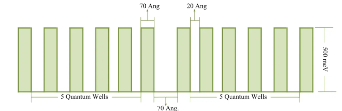
Consider the structure with the parameters displayed in Table 4.1 and illustrated in Figure 4.3.
Number of Quantum Wells 5
Central Quantum Well Width 70 Ang.
Superlattices of Quantum Wells Width 20 Ang.
Barriers Width 70 Ang.
Barriers Height 500 meV
Table 4.1: Parameters of superlattice of quantum wells structure.
4.1. Problem Definition 23
70 Ang. 5 Quantum Wells
500 m
eV
20 Ang
5 Quantum Wells 70 Ang
Figure 4.3: Superlattice of quantum wells structure example.
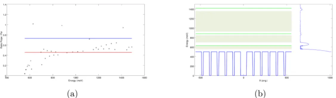
Degani and Maialle [2010]. After this, a visual observation by an expert is made to localize the discrete energy levels and minibands using the transmission plot. Figure 4.4 shows the transmission plot of the superlattice of quantum wells example. The discrete energy levels (in red), and the minibands (the regions inside the green rectangles) are shown.
Figure 4.4: Transmission of superlattice of quantum wells structure example.
Obviously, this task is empirical, prone to errors and slow, demanding an extensive knowledge and intuition of experts.
For this reason, an approximate method to accomplish automatically the energy-band configuration of the superlattices of quantum wells was developed and imple-mented, as described below.
24
Chapter 4. Optimization of Superlattices With Central Quantum Well
of the wave function is computed in the quantum wells of the superlattice and in the central quantum well, see Figure 4.5, to verify its localization, according to:
PSR =
Z
Superlattice
|ψ(x)|2 dx (4.1)
PCQW =
Z
CQW
|ψ(x)|2 dx (4.2)
wherePSR and PCQW are the square modules of the wave function,ψ(x), in the
super-lattice and in the central quantum well, respectively.
Figure 4.5: Localization of the wave function.
Once this is done, the ratio r = PCQW
PSR is calculated. Note that when the wave
function is localized closer to the quantum central well,rhas a greater value than that when localized in the superlattice, therefore, the maximum point can be considered as a discrete energy level.
Finally, the mean and the standard deviation are computed, and the following factor is calculated:
f =µ+λσ (4.3)
4.1. Problem Definition 25
4.6a shows the simulation result of the above procedure. Each point represents the ratio of the maximum points, red line the mean and the blue line the factor f. Figure 4.6b illustrates the energy-band configuration with the localized energy levels and the transmission coefficient of the SPQW example.
(a) (b)
Figure 4.6: Simulation result of superlattice example. The aproximate method result in (a) and (b) the final energy-band configuration.
Table 4.2 exhibits the energy values of the discrete energy levels and minibands detected by the algorithm.
Energy Value Localizated State
555.25 Beginning of Miniband
615.07 End of Miniband
628.22 Discrete Energy Level
697.35 Beginning of Miniband
845.08 End of Miniband
879.46 Discrete Energy Level
924.12 Beginning of Miniband
1354.92 End of Miniband
1414.28 Discrete Energy Level
Table 4.2: Fitness calculation example.
26
Chapter 4. Optimization of Superlattices With Central Quantum Well
4.2
Optimization Model
To accomplish the correct function of the GA, two fundamental details are important: the chromosome and the fitness function.
The chromosome of an individual is the abstraction of the parameters to be optimized in the real world problem. Thus, the chromosome to achieve the SPQW optimization is composed by 5 genes as illustrated in the Figure 4.7 and detailed in Table 4.3. For the structures studied in this work the numbers of quantum wells is a symmetrical parameter, i.e, the number of the quantum wells to the right of the central quantum well are the same in the left. For example, 5 quantum wells indicate that the structure will be composed by the central quantum well and 5 quantum wells to the right and to left of it, as detailed in the example of the Section 4.1.2.
Gene 1 Gene 2 Gene 3 Gene 4 Gene 5
Figure 4.7: Chromosome representation.
Table 4.3 explains the boundary conditions of the individual parameters, these ranges were defined in talks with professor Marcelo Maialle.
Gene Description Ranges
g1 Number of Quantum Wells [ 5 , 15 ]
g2 Central Quantum Well Width (Ang.) [ 10 , 40 ]
g3 Barriers Width (Ang.) [ 20 , 90 ]
g4 Barriers Height (meV) [ 400 , 600 ]
g5 Superlattice of Quantum Wells Width (Ang.) [ 20 , 70 ]
Table 4.3: Individual parameters and their boundary conditions.
In order to simplify the optimization process all variables are limited to real num-bers ranging from 0 to 1 which are latter interpolated to match superlattice attributes. To evaluate each individual the method described in Section 4.1.2 is used and the following fitness function is computed:
F itness(E(g1,g2,g3,g4,g5), X(g1,g2,g3,g4,g5)) =
X
(1−xi)·(ei−ei−1) +x·θ(ei−ei−1) (4.4)
4.2. Optimization Model 27
value of the ith beginning of miniband detected, xi = 0 if the energy value ei−1 is a discrete level, or xi = 1 if ei−1 is the end of a miniband,θ is an empirical parameter to penalize the error when not desired structures are found.
Thus, the fitness calculation for the same structure example explained in the Section 4.1.2 and for θ= 1.5, is detailed above:
F itness(E(5,70,70,500,20), X(5,70,70,500,20)) = ((555.25−500)·1.5)+(697.35−628.22)+(924.12−879.46) = 140.70 (4.5)
For the cases in that the first energy level is the beginning of a miniband, as evidenced in this example, the height of the barriers is used as reference to calculate the gap between them.
Then, the optimization target of the GA is to minimize the F itness function, formally:
Solution=min(F itness(E(g1,g2,g3,g4,g5), X(g1,g2,g3,g4,g5))) (4.6)
Once defined, the genetic algorithm, initially, creates a set of randomly generated individuals to compose the initial population. Individuals are then evaluated and selected based in their fitness to create couples and have their genes crossed to generate new individuals. Thus, each couple selected perform the crossover procedure where each gene for each son is computed according to:
Son1 =R·P arent1 + (1−R)·P arent2 (4.7)
Son2 = (1−R)·P arent1 +R·P arent2 (4.8)
where R is a random value between 0 and 1.
This crossover is always performed when new individuals are needed to create a new population. In order to broaden the search, these new individuals generated are randomly chosen to perform mutation. In the mutation process, genes are chosen to receive a new value. It has been applied, in this work, three kinds of mutation: uniform mutation, non-uniform mutation and side-shift mutation.
28
Chapter 4. Optimization of Superlattices With Central Quantum Well
value.
v′ =
v+δ(t, U B−v), if random value 0
v−δ(t, v−LB), if random value 1
(4.9)
whereLB and U B are lower and upper domain bounds for variablev. trepresents the generation number. The function δ(t, y), described in equation 4.10 returns a value in the range [0, y] that rapidly approaches 0 as the end of generations draws near. In this way, we allow our search to spread in the space initially and very locally at later stages; thus tunning the search to minor steps, which brings benefits when minimum and maximum can be very near on the search space.
δ(t, y) =y·(1−r(1−τt) b
) (4.10)
In this equation, t is the current generation, y is the maximum value that the function can return, r is a random number from [0..1], τ is the maximal generation number, andb is a system parameter determining the strengh of the shift that is going to happen in the gene.
Finally, elitism is ensured by always copying a number of best individuals from the last generation to the current generation.
4.3
Simulation Results
To find superlattices of quantum wells structures with specific energy-band configura-tion, the genetic algorithm described in Section 4.2 has been applied in conjunction with the simulation method explained in Section 4.1.2.
The parameters used to set up the GA, for all experiments, are detailed in Table 4.4.
Number of individuals per generation 50
Number of generations 150
Elitist set length 5
Mutation rate 15%
Uniform mutation rate 50%
Non-uniform mutation rate 50%
Table 4.4: Genetic algorithm parameters
4.3. Simulation Results 29
an elitist behavior, thus, preserving the evolution of the population.
The mutation rates described above means that 15% of the newly generated individuals are chosen to be mutated and among those, 50% are going to be uniformly mutated and the other 50% will be non-uniformly mutated.
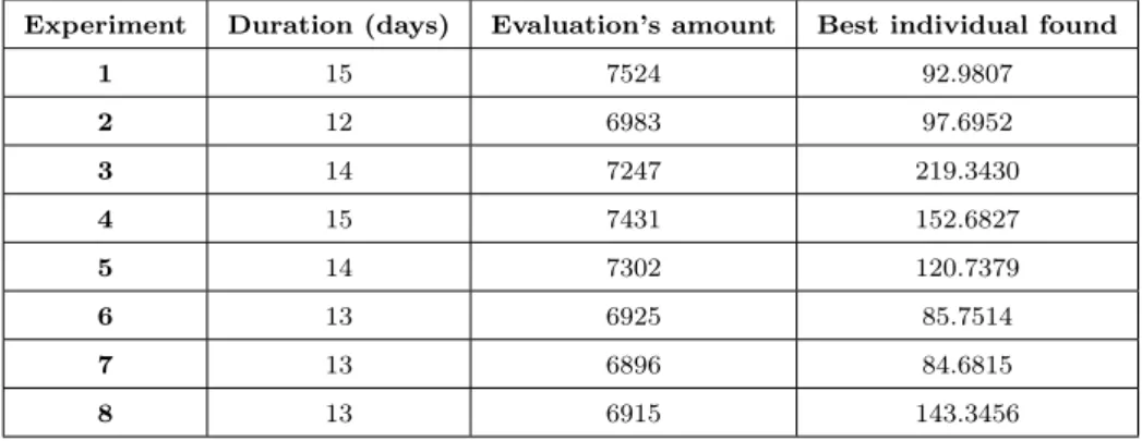
By applying these parameters in the genetic algorithm, during the course of three months it was possible to run eight experiments whose details are displayed in Table 4.5. For each experiment is detailed, the duration in days, the number of individuals evaluated and the the best fitness found. These experiment were performed in a machine with Ubuntu 12.04, 16 GB of memory RAM and processor Intel Core i7-2600 CPU a 3.40GHz. A superlattice of quantum wells simulation is carried-out in about 3 minutes.
Experiment Duration (days) Evaluation’s amount Best individual found
1 15 7524 92.9807
2 12 6983 97.6952
3 14 7247 219.3430
4 15 7431 152.6827
5 14 7302 120.7379
6 13 6925 85.7514
7 13 6896 84.6815
8 13 6915 143.3456
Table 4.5: Experiment results.
For these experiments two different values of the penalization in the fitness func-tion were used. In this way, for the experiments 1,2,3 and 4 θ was set in 0.6 and for the other experiments was set in 1.5. An important note is that when the θ value was set in 0.6, structures with not desired energy-band configurations were found.
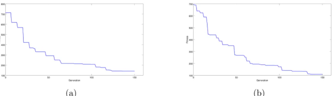
Figures 4.8a and 4.8b are results of the fitness curves, for the θ values of 0.6 and 1.5, respectively. In these curves, it is shown how each strategy evolved in an average of the best individuals from each generation.
The parameters of the best structure found in these experiments are shown in Table 4.6. In Table 4.7, the energy levels detected and the fitness value of this structure are detailed. Figure 4.9 illustrated the energy-band localization and the transmission coefficient for this structure.
30
Chapter 4. Optimization of Superlattices With Central Quantum Well
(a) (b)
Figure 4.8: Genetic algorithm evolution (a) with penalization 0.6. and (b) 1.5.
Number of Quantum Wells 7
Central Quantum Well Width 63 Ang.
Superlattices of Quantum Wells Width 16 Ang.
Barriers Width 48 Ang.
Barriers Height 501 meV
Table 4.6: Parameters of the best individual found.
Energy Value Localizated State
547.12 Discrete Energy Level
612.23 Beginning of Miniband
774.97 End of Miniband
862.08 Discrete Energy Level
881.65 Beginning of Miniband
1163.71 End of Miniband
Fitness Value 84.6815
Table 4.7: Simulation result of the best individual found.
Number of Quantum Wells 8
Central Quantum Well Width 62 Ang.
Superlattices of Quantum Wells Width 16 Ang.
Barriers Width 51 Ang.
Barriers Height 495 meV
Table 4.8: Parameters of the worst individual found.
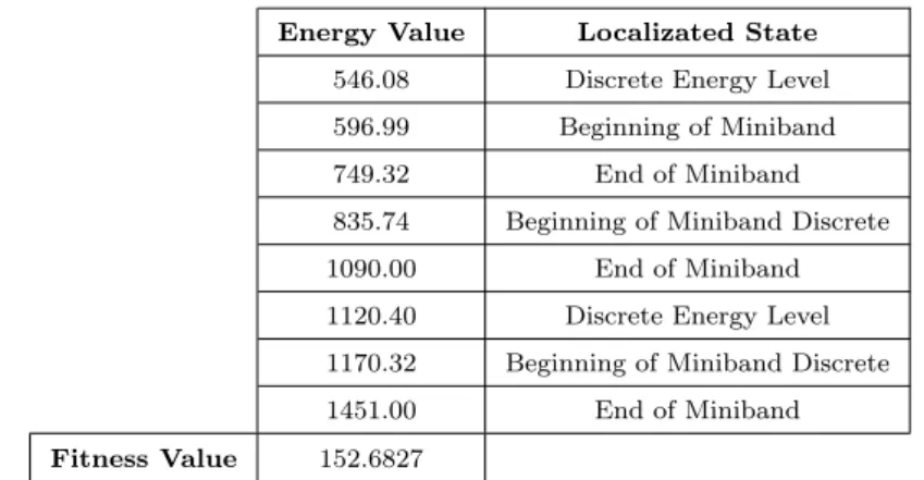
4.3. Simulation Results 31
Figure 4.9: Energy-band localization of the best individual.
Energy Value Localizated State
546.08 Discrete Energy Level
596.99 Beginning of Miniband
749.32 End of Miniband
835.74 Beginning of Miniband Discrete
1090.00 End of Miniband
1120.40 Discrete Energy Level
1170.32 Beginning of Miniband Discrete
1451.00 End of Miniband
Fitness Value 152.6827
Table 4.9: Simulation result of the worst individual found.
32
Chapter 4. Optimization of Superlattices With Central Quantum Well
Chapter 5
Logic Devices with Photonic
Crystals
This chapter presents the process to accomplish the all-optical logic gates in photonic crystals, the results of the Majority and Feynman gates proposed in this work and a methodology to be applied for the robustness analysis of all-optical logic devices in photonic crystals.
5.1
Majority and Feynman Gates
The realization of the logic gates can be achieved due to the photonic crystal waveguide, which takes advantage of the controlled light beam interference effect. For the devel-opment of all-optical Majority and Feyman gates, we use a two-dimensional photonic crystal.
According to wave optics theory, if the phase difference between two light beams is 2kπ (wherek = 0,1,2, ...), then constructive interference will occur, and the output light will have high power (corresponding to the logic state of 1). If the phase difference is (2k + 1)π (where k = 0,1,2, ...), then destructive interference will occur, and the output light will be approximately zero (corresponding to the logic state of 0) Zeng et al. [2010].
Photonic crystal structures studied here are composed of triangular lattice ar-rays of cylindrical silicon rods embedded in a background medium of air. The lattice constant a is 875 nm and the diameter of the silicon rods are 495 nm. The dielec-tric constant of silicon and air are set as 11.56 and 1, respectively. The wavelength,
λ, supported by the waveguide of this structure, corresponding to the photonic band
34 Chapter 5. Logic Devices with Photonic Crystals
gap, is 1550 nm, as used in the optical communications window. These are the same parameters used by Fu et al. [2013].
For the study of the electric field distribution of the photonic crystal structure, the simulations were carried out with the finite difference time-domain (FDTD) method using the MIT software package, MEEP, described by Oskooi et al. [2010]. MEEP can solve numerically Maxwell’s equations, used to calculate transmission and reflection spectra, resonant modes and frequencies, and field patterns (e.g. Green’s functions) in response to an arbitrary source, typically a continuous (CW) or Gaussian wave input. Also, MEEP will discretize this structure in space and time, and that is specified by a single variable, the resolution. The resolution used here was set as 40.
To set a logic input in 1a CW, with frequency ac
λ (c= 1) for units in MEEP, is
applied. Finally, to get the transmission output, the flux spectra is computed in the output point of the structure with the design of the logic device (Fd) and without it
(Fwd), then the ratio Fd/Fwd is calculated.
5.1.1
Majority Gate
The Majority gate is a logic device with three inputs and one output. The output is the majority function, thus, if at least two inputs are 0 then the output is 0. In contrast, the output is 1if and only if at least two inputs are 1. Table 5.1 present the truth table for this logic function.
A B C Y
0 0 0 0
0 0 1 0
0 1 0 0
0 1 1 1
1 0 0 0
1 0 1 1
1 1 0 1
1 1 1 1
Table 5.1: Majority gate truth table.
5.1. Majority and Feynman Gates 35
The schematic structure for the all-optical Majority gate is shown in Figure 5.1a. It is formed by three symmetrical optical waveguides: AY, BY, CY, of equal length.
A B C Y (a) 1 0 0 0 (b) 0 1 0 0 (c) 0 0 1 0 (d) 0 1 1 1 (e) 1 0 1 1 (f) 1 1 0 1 (g) 1 1 1 1 (h)
Figure 5.1: Majority gate simulation results.
36 Chapter 5. Logic Devices with Photonic Crystals
Y. There are losses in the way, reaching output Y with transmission smaller than 0.35. These correspond to a logic operationM aj(1,0,0) = 0, as shown in Figure 5.1b.
Similarly, if a single beam is injected into input port B or C, the signal light can propagate through the optical waveguide BY and CY, respectively, to the output Y with low transmission. These correspond to logic operations M aj(0,1,0) = 0 and
M aj(0,0,1) = 0, as shown in Figure 5.1c and Figure 5.1d.
When two beams are injected into two inputs ports, then the phase difference of these two signal light beams is zero. Constructive interference occurs, and the output signal has a transmission greater than 0.85, as shown in Figure 5.1e, Figure 5.1f and Figure 5.1g. This corresponds to the logic operations M aj(0,1,1) = 1, M aj(1,0,1) = 1, M aj(1,1,0) = 1.
Finally, if the beams are injected into the three inputs ports, then the phase difference at the cross point is zero, causing a constructive interference, and achieving 1.00 of transmission. This corresponds to M aj(1,1,1) = 1, shown in Figure 5.1h. Obviously, when no single beam is injected in any input port, then no light comes to output, corresponding toM aj(0,0,0) = 0.
Table 5.2 summarizes the transmission results for the Majority gate. When the transmission output is greater than 0.85 it is considered as logic output 1. If the transmission output is less than 0.35, then it is considered as logic output 0.
Input (A,B,C) Output Y Transmission
(0,0,0) 0 0
(0,0,1) 0 0.32
(0,1,0) 0 0.32
(0,1,1) 1 0.88
(1,0,0) 0 0.32
(1,1,0) 1 0.95
(1,0,1) 1 0.95
(1,1,1) 1 1.00
Table 5.2: Transmission results for all-optical majority gate
5.1.2
Feynman Gate
In 1961, Rolf Landauer argued that any irreversible computational process, e.g., AND, OR, XOR, implies the loss ofKBT Ln2joules per bit erased, whereKBis the Boltzmann
5.1. Majority and Feynman Gates 37
known as reversible gates, are information preserving, i.e., they have one-to-one relation (bijective functions) between inputs and outputs.
The Feynman gate is a logic reversible device with two inputs (A,B) and two outputs (X,Y). The outputs are defined by the function X =A andY =A⊕B. Table 5.3 illustrate the truth table for the Feynman logic gate.
A B X Y
0 0 0 0
0 1 0 1
1 0 1 1
1 1 1 0
Table 5.3: Feynman gate truth table.
Photonic crystals have been seen as a promising technology for approaching the thermodynamic limit of computation, thus in an effort to go beyond that limit we pro-pose an all-optical Feynman gate, shown in Figure 5.2a. To the best of our knowledge, it is the first time that a reversible gate is proposed based on photonic crystals.
A
B
X
Y
(a) 1 0 1 1 (b) 0 1 0 1 (c) 1 1 1 0 (d)Figure 5.2: Feynman gate simulation results.
38 Chapter 5. Logic Devices with Photonic Crystals
and Y, with transmission of 0.10 and 0.50, respectively. This corresponds to the logic operationF eyn(0,1) = (0,1), as shown in Figure 5.2c.
When the two input ports are excited, then the difference of the path length between the waveguide AY and BY is one lattice constant, and the phase difference is π. Thus, destructive interference occurs and the transmission in the output Y is only 0.01. The transmission at the output X is 0.75. This corresponds to the logic operation F eyn(1,1) = (1,0), as shown in Figure 5.2d. Finally, if no single beam is injected in both input ports, then no light comes to the output, corresponding to
F eyn(0,0) = (0,0).
Table 5.4 presents the results for the transmission of the all-optical Feynman gate. It is possible to observe that transmissions ≥ 40% are considered as logic output 1, and ≤10% are considered as logic 0.
Input (A,B) Output (X,Y) Transmission X Transmission Y
(0,0) (0,0) 0 0
(0,1) (0,1) 0.10 0.50
(1,0) (1,1) 0.45 0.40
(1,1) (1,0) 0.75 0.01
Table 5.4: Transmission results for all-optical Feynman gate
5.2
Robustness Analysis of All-Optical Logic Gates
The process of robustness analysis proposed here is a methodology to identify critical regions and evaluate the reliability and fault tolerance of the all-optical logic devices designed with photonic crystals waveguides. This is a relevant step before the physical growth of these devices, because allows to know and measure the behaviour of them due to possible errors or disorders added in the system.
Generally, the logic gates projected in two-dimensional photonic crystals are com-posed of triangular or square lattice arrays of cylindrical semiconductor rods embedded in a background medium of air. On the other hand, they also can be projected with triangular or square lattice arrays of cylindrical air holes embedded in a background medium of a semiconductor material. The disorders consist in horizontal and vertical displacements, reduction and enlargement of the cylinders that form the device.
Then, to cause disorders in the system, random numbers are generated with the following Gaussian distribution:
5.2. Robustness Analysis of All-Optical Logic Gates 39
where a= 1
σ√2π, b =µ, c=σ and x the input, µand σ are the center and the width
of the function, respectively, as can be observed in the Figure 5.3.
Figure 5.3: Gaussian distribution for σ= (0.5,1.0,5.0,10.0,15.0,20.0).
This distribution allows to control the µ and σ parameters. In this work, µ is setted as 0 and σ a set of variable parameters: (0.5,1.0,10.0,15.0,20.0). It is impor-tant to note that bigger σ values can cause uncontrollable behaviours in the system. Thus, the formal expression that describes the disorder added to a cylinder for each component is:
f(x, y, r) = (x±δx(0, σ))x+ (y±δy(0, σ))y+ (r±δr(0, σ))r (5.2)
where x and y are the cartesian coordinates of the cylinder position and r the radius. It is important to remark that δ(0,20) generates disorders about±80 nm.
When these disorders appear in the growth and/or fabrication process, the correct operation of the device probably will be affected. That is, the output transmission ex-pected values can change significantly. To consider an error in the output transmission a tolerance value is defined, setted in 0.1, as in electronic devices. So, for each study case of each logic gate, 50 simulations are performed, as indicated by Jain [1991], and a statistical test is computed to measure the reliability and robustness of the device. The statistical test consist in calculate the mean, standard deviation and confidence interval with 95% of confidence level for each study case. Then, the tolerance value is evaluated with respect to the expected value.
40 Chapter 5. Logic Devices with Photonic Crystals
as logic 0, but the obtained expected value includes includes smaller values that the tolerance, (0.7 for this case), it can be said with 95% of confidence level that the logic device probably operates unexpectedly, as shown in Figure 5.4b.
Co nf id en ce In te rv al
For 0 logic value
0.15 0.25 0.28 -0.05 0.12 (a) Co nfi de nc e I nte rv al
For 1 logic value 0.95
0.55
0.78
0.70 0.80
(b)
Figure 5.4: Robustness Analysis test. (a) for output transmission interpreted as logic 1 and (b) logic 0.
5.2.1
OR Gate
To accomplish the robustness analysis of the OR logic device proposed by Fu et al. [2013], the first three study cases are illustrated in Figure 5.5.
It is important to remember that the OR is a symmetrical logic device, i.e., the transmission and the path difference are equal for the inputs, (0,1) and (1,0). The output transmission for(0,1)−(1,0)input cases is: 0.411and for input(1,1)is0.846. Then, output transmission greater than 0.4 and is considered as logic 1. The lower boundary of the tolerance to consider an error is 0.3.
5.2. Robustness Analysis of All-Optical Logic Gates 41 Line 2 Line 1 Line 3 Line 2 Line 3 Line 1
Figure 5.5: Lines analysed for the OR device.
(0,1) (1,1)
σ σ
Region 0.50 1.00 5.00 10.0 15.0 20.0 0.50 1.00 5.00 10.0 15.0 20.0
Mean 0.411 0.411 0.411 0.408 0.385 0.335 0.846 0.846 0.845 0.833 0.773 0.450
Std 0.002 0.004 0.019 0.044 0.076 0.181 0.002 0.003 0.016 0.037 0.095 0.276
0.408 0.402 0.375 0.322 0.237 -0.019 0.841 0.840 0.814 0.760 0.587 -0.091 All
CI
0.415 0.420 0.447 0.495 0.534 0.689 0.850 0.852 0.876 0.905 0.959 0.990 Mean 0.409 0.409 0.408 0.402 0.382 0.313 0.841 0.841 0.836 0.808 0.763 0.530
Std 0.002 0.004 0.020 0.033 0.094 0.187 0.002 0.003 0.017 0.041 0.107 0.237
0.405 0.401 0.368 0.337 0.198 -0.053 0.838 0.834 0.802 0.729 0.553 0.065 Line 1
CI
0.413 0.417 0.448 0.467 0.566 0.679 0.845 0.847 0.870 0.888 0.974 0.995 Mean 0.411 0.411 0.411 0.412 0.411 0.399 0.846 0.846 0.846 0.846 0.852 0.820
Std 0.000 0.000 0.002 0.004 0.007 0.071 0.000 0.001 0.002 0.005 0.026 0.091
0.411 0.410 0.407 0.404 0.397 0.259 0.845 0.845 0.842 0.837 0.801 0.641
Line 2
CI
0.412 0.412 0.415 0.419 0.426 0.539 0.846 0.847 0.850 0.856 0.903 0.999
Mean 0.411 0.411 0.411 0.411 0.411 0.409 0.846 0.846 0.846 0.846 0.846 0.842
Std 0.000 0.000 0.000 0.000 0.001 0.006 0.000 0.000 0.000 0.000 0.001 0.008
0.411 0.411 0.411 0.411 0.409 0.397 0.846 0.846 0.846 0.846 0.844 0.826
Line 3
CI
0.411 0.411 0.411 0.411 0.412 0.421 0.846 0.846 0.846 0.846 0.847 0.858
Table 5.5: Simulations results for the modifications of the all cylinder and the first three lines for the OR device. Std is the standard deviation and CI the confidence interval.
For the input(0,1)when all cylinders are modified withσ = [15,20]the expected transmission value includes 0.3. Then the lower boundary of tolerance is infringed as a result of a high standard deviation, due to low transmission values obtained. Thus, with 95% of confidence level, it can be said that the system probably operates unexpectedly. When the disorders are added using (0.5≤ σ ≤ 10) the performance of the device is not affected, at the same confidence level.
If the disorders are added in the first line the same considerations are valid.
![Figure 2.5: Two dimensional photonic crystal. Taken from Joannopoulos et al. [2008].](https://thumb-eu.123doks.com/thumbv2/123dok_br/15211186.21297/35.892.249.656.660.786/figure-dimensional-photonic-crystal-taken-joannopoulos-et-al.webp)
![Figure 3.1: Schematic structure for AND logic gate proposed by Rani et al. [2013].](https://thumb-eu.123doks.com/thumbv2/123dok_br/15211186.21297/41.892.333.579.458.633/figure-schematic-structure-logic-gate-proposed-rani-et.webp)
![Figure 3.2: Schematic structure for AND logic gate proposed by Yang et al. [2013].](https://thumb-eu.123doks.com/thumbv2/123dok_br/15211186.21297/42.892.310.557.158.326/figure-schematic-structure-logic-gate-proposed-yang-et.webp)