Distribution Function Estimation of the
Timing Jitter in Sample Rate Converter
Manish Sabraj, Vipan Kakkar
School of Electronics & Communication Engg.
Shri Mata Vaishno Devi University, Jammu and Kashmir (India)
Abstract:- The aim of digital sample rate conversion is to bring a digital audio signal from one sample frequency to another. The distortion of the audio signal introduced by the sample rate converter should be as low as possible. The generation of the output samples from the input samples may be performed by the application of various methods. In this paper, a new technique of digital sample-rate converter is proposed. We perform the analysis for distribution function estimation of the timing jitter in proposed digital sample rate converter.
I. INTRODUCTION
The increasing need of processing digital data at more than one sampling frequency has resulted in the development of a new area of digital signal processing known as multirate signal processing. The basic operations in multirate signal processing are decimation and interpolation ([1]-[3]). Decimation reduces the sampling rate effectively by compressing the data and retaining the desired information. Interpolation increases the sampling rate. Sampling rate conversion can be done either in analog domain or in digital domain. In the first method, the digital signal is passed through a digital-to analog converter (DAC) and then the analog signal is resampled at the desired rate. In the second method, the resampling of digital data at the desired rate is carried in the digital domain itself. In this paper, analysis results are shown for a new method of digital sample rate converter.
The operation principle of the new method of sample rate conversion is very simple. An input sample is directly transferred to the output, while per unit of time, a certain amount of these samples is omitted or repeated, depending on the difference in input and output sample frequencies. The omission, acceptance or repetition of a sample is called ‘validation’. In order to get the simplest hardware implementation, the choice has been made to use only the take-over operation and the repetition operation in the current system solution. This means that the output sampling frequency of the
sample rate converter is always larger than the input sample frequency.
The process of repeating samples inevitably introduces errors. The resulting output samples will have correct values, but as a result of the validation operation, they are placed on the output time grid with a variable time delay with respect to the input time grid. As a consequence, the output sequence should be viewed as the input sequence, having the correct signal amplitude, which is sampled at wrong time moments. The effect is the same as sampling the input signal by a jittered clock. As a result, it can be stated that the time error mechanism introduced by the validation algorithm is time jitter.
If all input samples would be transferred to the output grid without the repetition or omission of a certain amount of them, then the output signal would be just a delayed version of the input signal, exhibiting the same shape. It is the repetition and omission (in the current system setup only the repetition ) of input samples that give rise to a variation in time delay for each individual output sample. This variation in individual time delays introduces phase errors. As a result of this, the shape of the output signal will be distorted.
phase modulation terms can be filtered by a decimation filter or an analog low-pass filter which is directly placed after the sample-rate converter. Figure 1 shows the block diagram of the complete sample-rate converter.
Figure 1. Block diagram of the sample-rate converter
As has already been mentioned, only the input sample take over operation will be employed here in order to get the simplest hardware. This means that the input sample frequency of the converter must be always be smaller than the output sample frequency. With this restriction imposed, it is assured that all input samples are used in the output sequence, none of them being omitted. The extra output samples per unit of time are inserted in the output sequence by repetition of their previous output samples. II. TIME JITTER SIGNAL CONSTRUCTION
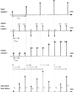
In a proposed sample rate conveter, the output samples are placed on the output time grid with a variable time delay, which results in time jitter. Due to this timing jitter, the output samples will not have the correct amplitude [4]. Each output sample has an individual delay, with respect to the previous input sample, when it is placed in the output sequence. This time difference is called timing jitter. In figure 2 a plot is given which shows a part of an input sequence, a conversion control signal (output of sigma-delta converter), the converted output sequence and the individual time delays of the output samples ( time jitter signal).
Let Ts,in and Ts,out be the sample period of the
input sequence and the output sequence respectively. Assume that the PLL supplies a
certain DC to the sigma-delta modulator, such that its output pulses are as shown in figure 2. The output samples of the sample-rate converter can then easily be constructed by applying the conversion control algorithm given in table 1. It should be noticed that the output time grid is determined by the output pulses of the sigma-delta modulator.
Figure 2. An overview of the sample-rate conversion process in the time domain
CONVERSION CONTROL IN THE SAMPLE-RATE CONVERSION PROCESS
Sigma-delta output
Control Action
-1 Take over a new input sample
1 Repeat the previous output
sample
III. DISTRIBUTION FUNCTION ESTIMATION OF THE TIMING JITTER
The output sequence of a first order sigma-delta modulator is fixed for a given DC input, that is, when the DC level at the input is for instance 0.5 Volts, then the output sequence is a fixed pattern, only consisting of repetitions of the sequence “111-1”.
The output sequence of a higher-order sigma-delta modulator is not fixed, it also contains patterns differing from the above mentioned. For third and higher-order sigma-delta modulators, the diversity of the patterns is such that an exact analysis is not available because of its complexity. In order to simplify the analysis, we will have to make a few assumtions. It is observed that a repetition sample causes an increment in time delay of Ts,out seconds. When
an output sample is for instance repeated n times, the n-th repetition sample has an increment in time del ay of n.Ts,out seconds with respect to the
first repetition sample. When the output sampling frequency is kept constant, it is to be expected that the maximum possible value of the time delay is larger when the input sampling frequency is smaller, because a small input sampling frequency implies much repetitions (more “1” pulses).
We now make the assumption that the average delay of the copied input samples is zero, so the output samples obtained by copying the input samples have on the average the correct timing moment. As a consequence, its only the repetition output samples that have on the average a contribution to the absolute value of the time delay.
In one second Fs,in input samples are copied to
the output. The remaining Fs,out-Fs,in output
samples are repetition samples. The average number of repetitions of each input sample equals:
1
, , ,
,
,
in s
out s in
s in s out s av
F
F
F
F
F
R
(1) Since a repetition output sample introduces anincrement in time delay of Ts,out this corresponds to an average time delay of:
out s in s out s in s out s in s
out s
av T T
F F T F F
T , ,
, , , ,
, 1 1
.
1
(2)
Equation (2) shows that at lower input sampling frequencies the average time delay of the output samples is larger, which satisfies the expectations.
We want to determine the second moment (variance) and the fourth moment of the time delay, so we are confronted with the diversity in the output patterns of the sigma-delta modulator. We expect that when the order of the sigma-delta modulator is higher, the variance of the time error is larger. This is because a higher-order sigma-delta modulator produces a larger variety in output patterns. The most evident thing to do is to estimate the distribution function by means of simulation results.
IV. NUMERICAL ANALYSIS
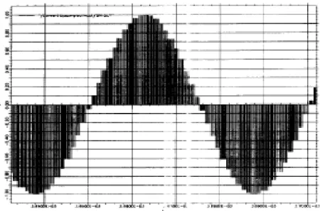
A third-order sample-rate converter has been simulated using 131072 simulation points. The output sampling frequency is fixed at 128Fs,out while the input sampling frequency equals 19.23Fs (Fs=44.1kHz). It is calculated that the
DC level at the input of the sigma-delta converter must be +0.69953125 Volts, which is about the upper bound of the usable input range. From (2) it follows that in terms of time delay, this is the worst case situation.
In figure 3 a plot of the corresponding converted sinewave is given. From this plot it follows that the repetition sequences of the input samples are subject to fluctuation. These fluctuations are caused by the diversity in the output patterns of the sigma-delta modulator.
Figure 3. An example of a converted sinewave. The input sampling frequency equals 19.23 Fs while the output sampling frequency equals 128 Fs.
TABLE II
DISTRIBUTION FUNCTION OF TIME DELAYS
Number of Repetition s
R
Number of occurance s
Probability P(Ri=R)
(1≤i≤#input_sample s)
1 0 0
2 3 0.000152354
3 575 0.029201158
4 3224 0.163729623
5 5487 0.278655223
6 5424 0.275455792
7 3292 0.167182977
8 1454 0.073840841
9 223 0.013249708
10 9 0.000457062
>10 0 0
Figure 4 shows the distribution function of the repetition sequences of the output signal of the sigma-delta modulator. Note that this distribution function resembles the well-known Gaussian distribution.
From table 2 the average time delay (first moment) can be calculated:
sec
00
.
1
10
77
.
1
.
66
.
5
...
...
.
)
(
.
7
,
i souti
i
P
R
R
T
R
t
E
(3)
Figure 4. Distribution function of the time delays obtained by a simulation
When the values of the sampling frequencies are filled in (2), it follows that this equation predicts exactly the same average delay as the one obtained by simulation results.
This average time delay will not give rise to amplitude deviations in the output signal. It’s the fluctuations in time delay that are responsible for the amplitude errors.
2 14 2 , 2 , 2sec
10
19
.
5
.
65
.
1
...
...
)
(
.
).
66
.
5
(
out s i i out s iT
NR
delay
P
T
NR
t
E
t
E
(4) The standard deviation is the square root of the variance and equals:sec
228
.
0
.
28
.
1
...
...
.
65
.
1
, 2 , 2
out s out s t tT
T
(5)For the fourth moment we find from the simulation results:
4 27 4 , 4 , 4sec
10
02
.
7
...
...
.
13
.
7
)
(
...
.
).
66
.
5
(
out s i i out s iT
NR
delay
P
T
NR
t
E
t
E
(6)Finally, when we substitute (4) and (5) in the first order approximation equations, the second moment of the amplitude error and the error of the first –order approximation become:
2 14 2 2 2 ^ 2 2 2 2 ^
.
10
19
.
5
.
.
.
3
4
...
...
}
)
(
{
.
.
.
.
3
4
))
(
(
)
(
x xW
t
t
E
W
t
t
t
x
t
x
E
(7) 2 27 4 4 4 ^ 2 4 4 ^ 2.
10
02
.
7
.
.
.
5
4
...
...
}
)
(
{
.
.
.
.
5
4
...
...
)]
(
).[
(
.
2
1
x xW
t
t
E
W
t
t
t
x
E
(8)When we divide (8) by (7) we obtain the relative error of the first-order approximation. This relative error εrel becomes, when we assume that
the signal x(t) has a bandwidth W of 20kHz (which is true for audio signals):
% 032 . 0 10 2 . 3 . . 10 12 .
8 142 2 4
W
rel
(9)
It appears that the worst case relative error caused by a first-order approximation is 0.032%. From this figure we may conclude that the first-order approximation of the amplitude error is
accurate enough to predict amplitude deviations as well as noise power introduced by the sample-rate coversion process.
In order to get some insight in the absolute value of the noise power we have to determine the variance of the input signal x(t).
V. CONCLUSION
In this paper it is observed that the digital sample-rate converter manifests itself as a jitter generator. The output samples are placed on the output time grid with a variable time delay. The time jitter signal has been constructed by applying the conversion control algorithm. The timing jitter causes amplitude deviations in the output signal. In this paper a first-order approximation of this amplitude error has been given based on a stochastic approach. It has shown that for the worst case situation, this first-order model is accurate enough to predict amplitude deviations as well as noise power introduced by the sample-rate converter (worst case relative error of 0.032%, worst case noise power 30.9 [dB] below signal power). The distribution function of the output repetition sequences of the sigma-delta converter resembles that of the Gaussian distribution.
REFERENCES
[1] R. Crochiere and L. Rabiner, Mullinale Digital Signal Processing., Englewood Cliffs, NJ: Prentice Hall, 1983.
[2] Schafer and Rabiner, “A digital signal processing approach to interpolation,”Proc. ZEEE, v. 61, pp 692-702, June 1973.
[3] M. G. Belanger et al., “Interpolation, Extrapolation, and Reduction of Computation Speed in Digital Filters,” IEEE Trans. Acoust., Speech, Signal Processing, v. ASSP-22, pp 231-235.
[4] Baggen, C.P.M.J., An Information Theoretic Approach to Timing Jitter, Doctoral Dissertation, University of California, San Diego. 1993.
[5] R. Fitzgerald and W. Anderson, “Spectral distortion in sampling rate conversion by zero-order polynomial interpolation,” IEEE Trans. Signal Processing, vol. 40, pp. 1576–1578, June 1992.
[6] Y. P. Lin and P. P. Vaidyanathan, “Periodically nonuniform sampling of bandpass signals,” IEEE Trans. Circuits Syst. II, vol. 45, pp. 340–351, Mar. 1998.
[7] Network Transmission Committee Report No. 7, June 1975,August 1974. Published by The Public Broadcasting Service.