Total secondary-electron yield of metals measured by a dynamic method
Carlos Alberto Fonzar Pintão and Roberto Hessel
Citation: Journal of Applied Physics 88, 478 (2000); doi: 10.1063/1.373682 View online: http://dx.doi.org/10.1063/1.373682
View Table of Contents: http://scitation.aip.org/content/aip/journal/jap/88/1?ver=pdfcov Published by the AIP Publishing
which the dielectric is irradiated continuously, have failed because the dielectric becomes charged and this charge interferes with the emission process. The dynamic method can, however, be applied to metals where volume charges are prevented. This article reports dynamic measurements of the total secondary emission yield from stainless steel, platinum, and aluminum and compares them with results from the current pulse method. In order to apply the dynamic method to metals a simple but important change in the setup was introduced: a dielectric slab was placed between the electrode and the metallic sample, which permitted the sample surface potential and therefore the energy of the incident electrons to change continuously. Unlike for dielectrics, the emission curves for metals are identical when obtained by the two methods. However, for a sample with deliberately oxidized surfaces the total secondary emission yield is smaller when measured with the dynamic method as compared with the pulse method, just as happens for dielectrics. © 2000 American Institute of Physics. @S0021-8979~00!03413-7#
I. INTRODUCTION
When irradiated by an electron beam, solid surfaces emit low-energy secondary and backscattered primary electrons. Numerous authors have investigated this effect and reviews of the problems addressed are found in several books and papers.1,2In order to quantify the emission process it is usual to define the total secondary yield~the ratio between emitted and incident electron number! and study its dependence on the incident beam energy as well as on the properties of the irradiated surface. The total secondary yield can assume val-ues smaller, equal to, or greater than one for irradiation en-ergies below a few keV. The surface of an irradiated dielec-tric becomes positively or negatively charged as the total yield differs from one. Such polarization can affect the emis-sion process. Most authors have irradiated dielectrics with short electron pulses, while at the same time measuring the electron emission by a separate conveniently poled collector electrode.3–5 A new, so-called dynamic method ~DM! has been discussed in the literature.6–8This method ~DM!8
was proposed to study the secondary electron emission from in-sulators in the planar symmetry: upon charging the insulator surface, the effective energy of the electron beam is changed, and from the knowledge of the beam current, current to the back electrode, and sample capacitance, the whole secondary yield can be obtained in suitably chosen runs. However, as anticipated, the accumulated charges do indeed interfere with the measurement, considerably decreasing the yield.9
We have found, however, that the DM may be success-fully applied to study secondary emission of metals provided a single and obvious change is made: the irradiated metal disk is placed on top of an insulating foil of very small thickness. With this arrangement the metal potential changes during irradiation owing to the rapid dissipation of excess charge to the back surface of the metallic disk facing the insulating foil, therefore avoiding interference between the beam and generated charges. For the sake of comparison measurements were also carried out using ~short! electron beam pulses~PM!9
without the back insulator foil.
II. EXPERIMENT
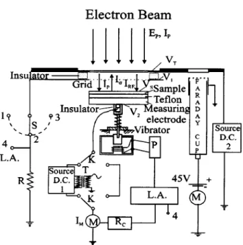
The setup used, schematically shown in Fig. 1, has al-ready been described in detail.9Its main features are:
~1! the beam energyEP ranges from 0.4 to 20 keV, and the
current IP from 1026 to 10210A, which is measured by
a Faraday cup;
~2! the beam scans an area greater than the sample area, with the sample being 3 cm in diameter;
~3! the grid–target geometry is plane, with grid transparency of approximately 80%;
~4! a meter measures the current IM to the back electrode
which may be grounded or biased to an adjustable po-tential V2 ~0–63 keV!;
~5! the back electrode vibrates against the grid~which in our measurements remained grounded! thus allowing the measurement of the potential10of the back electrode by means of a lock-in amplifier ~LA!method of the vibrat-ing capacitor; and
a!Author to whom correspondence should be addressed; electronic mail:
478
0021-8979/2000/88(1)/478/5/$17.00 © 2000 American Institute of Physics
~6! the sample is discharged by means of the electron beam under conditions that allow the performance of the ‘‘self-regulating mechanism’’.6,7
Teflon-FEP®samples 50mm thick, 5 cm diameter, pro-vided on both faces with a deposited aluminum layer, 3 cm in diameter, were put directly over the measuring electrode, supporting the metal samples~see Fig. 2!. These were;0.5 mm thick polished stainless steel and platinum disks. Mea-surements were also carried out with the electron beam im-pinging directly onto the deposited aluminum layer in order to compare the results with those of the same aluminum deposited film exposed deliberately to ambient atmosphere for a long time. A vacuum better than 1024
Pa~1 Torr51.33
Pa! was used. Our system was not developed to deal with metallic surfaces, for which ultrahigh vacuum is required as in usual surface physics experiments. Therefore, we cannot expect the yields obtained for metals to be comparable with known values in the literature. Our main intent is rather to illustrate the applicability of the dynamic method to metals, which is done as explained later.
A. DM measurements
In DM measurements we exploit the fact that upon con-trolling the electron yield s, one may charge samples posi-tively or negaposi-tively.
~1! Measurement accessing is in the energy range be-tween EI andEII, the first and second crossover points,
re-spectively. The beam energy is somewhat larger thanEIIand
the bias voltageV2so chosen that the effective initial energy
Eiis a little higher thanEI. For thisV2is made negative and
such that 2eV2,Ep2EI, e being the electronic charge.
The sample is charged positively, and its potential increases by VS causing the effective energy E to be equal to EP
1eVS. Finally the second crossover point EII is reached,
when charging ends. This is shown in Fig. 3, where EM is
the energy for maximum yield. The insert shows the current balance Is being the secondary current define as Is5IM
2IP, withIRE50. The yieldsis calculated from
s52Is
IP
512IM
IP
, ~1!
where the currents are considered negative downward~ there-fore IM in Fig. 3 is positive!.
~2!Measurement accessing energies belowEIand above
EII. In these cases V2 is made zero and EP is chosen,
re-spectively:~a!well belowEI, with charging finishing when
VS reachesVF ~filament potential!;~b!well above EII, with
charging finishing whenE5EP1eVS becomes equal toEII.
This is shown in Fig. 4.
FIG. 1. Scheme of experimental setup. ~M!: Keitley meter, ~T!: high-insulated coupling capacitor,~P!: signal generator for magnetic coil,~LA!: lock-in amplifier,~R!: measuring resistor for grid signals, (RC): double-pen recorder, (VS): surface potential, (V1, V2, andVT): polarization potential for grid, electrode, and cover, respectively; (IP, Is, IM, andIRE): current
of electrons incident, emitted, measuring, and recaptured, respectively, (EP): primary or incident energy of electrons.
FIG. 2. Support of the samples adapted to apply the dynamic method to metal.
FIG. 3. Total emission yieldsas function of energyE~schematic!.EIand EIIare first and second crossover points,sM is maximum yield, andEM energy of maximum yield. The continuous curve represents the section be-tweenEIandEIIobtained from dynamic method. Also shown are vectorial
representations of the currents (IP, Is, and IM) indicating the studied interval.
479 J. Appl. Phys., Vol. 88, No. 1, 1 July 2000 C. A. F. Pinta˜o and R. Hessel
B. PM measurements
Measurements with short pulses ~the pulse duration is not important! and with the metal disk functioning as the back electrode were carried out for comparison with DM results. In this method the beam energyEP is fixed and the
electrode potential V2 is adjusted, step by step, in order to
cover the desired range of energies.
III. RESULTS AND DISCUSSION
In Figs. 5–7 we show the yields as a function of the effective beam energyEfor a stainless steel disk, a platinum disk, and an aluminum deposited film for a beam current of 2.25 nA, but the results are essentially independent of this parameter. In each case, the results obtained with the PM are compared with those with the DM starting at different initial effective energies Ei, either to cover the desired range of
energies, as explained in Sec. II A, or for the sake of
illus-trating the reliability of the method. In all cases the curves are reasonably well superimposed on each other. This behav-ior indicates that possible impurities~such as an oxide layer on aluminum and platinum disks!, which should expect to be present since ultrahigh vacuum was not employed, do not affect the conductivity of the surface, at least as far as elec-tron emission is concerned. For insulating materials, the two methods indeed lead to different results. For instance, Hessel and Gross11 showed that for polymers s obtained with DM are smaller than with PM and depend onEi, which indicated
that charge accumulation over the polymer surface impairs the use of the DM method for insulating materials. There-fore, even if oxide layers were formed on the metal plates, they probably are unable to store considerable amounts of charges, as explained below.
FIG. 4. sas function of energyE~schematic!. The continuous curve rep-resent the sections aboveEIIand belowEIobtained from dynamic method.
Also shown are vectorial representations of the currents (IP, Is, andIM) indicating the interval studied.
FIG. 5. Total emission yield as a function of energy for a 0.5 mm stainless steel disk. Pulse method: section between EI50.020 keV and EII54.75
keV, Ep52.0 keV, 4.0 keV, V2 was selected from2100 to 22100 V.
Section aboveEII, Ep56.0 keV,V2521000 V. Dynamic method: section
betweenEIandEII, Ep52.0 keV,V2was selected in21980,21900, and
21800 V. In all casesIPwas 2.25 nA.
FIG. 6. Total emission yield as a function of energy for a 0.2 mm platinum disk. Pulse method: section betweenEI50.020 keV andEII57.0 keV,Ep 52.0 keV,V2was selected from2200 to21980 V.Ep54.0 keV,V2was
selected from2500 to22100 V andEP56.0 keV,V2was selected from
2500 to 22000 V. Dynamic method: section between EI and EII, Ep 52.0 keV,V2was selected in21980,21800,21600, and21200 V and Ep54.0 keV,V2was selected in22100 V;IP52.25 nA.
FIG. 7. Total emission yield as a function of energy for a 100 nm aluminum deposited film. Pulse method: section between EI50.020 keV and EII
53.0 keV, Ep52.0 keV, V2 was selected from 2200 to21950 V,Ep 53.0 keV, V2 was selected from 2200 to 21500 V. Section above EII, Ep54.5 keV,V2 was selected from 2500 to 21500 V. Dynamic
method: section between EI and EII, Ep52.0 keV, V2 was selected in
In a subsidiary experiment, the aluminum deposited film was exposed to ambient atmosphere for a long period of time. As expected an oxide layer developed, which now af-fected the yieldsconsiderably. The positive charge stored in the aluminum oxide layer prevent some low energy electrons
~‘‘true’’ secondary electrons! from escaping from the sur-face, thus leading to a smaller s in the DM method, as shown in Fig. 8. It is concluded that charges created during the emission process suffer much faster recombination in metals than in insulating materials, and therefore they do not modifys. The fact that emission curvess3E obtained from both methods are the same and the fact that sdoes not de-pend on the energy Ei of the impinging electrons show that
the depth at which charges are created within the sample or their mobility does not affect the results, unlike in polymers.11 This means that the charge recombination pro-cess, which gives origin to low energy electrons, is suffi-ciently fast not to interfere with the electrons that are emitted by the sample surface.
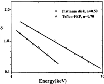
In summary, upon using the DM and PM methods inde-pendently, the sample behavior can be classified as that of a metal or insulator during the emission process. In order to reinforce this claim, we analyzed some of the results quanti-tatively. It is known that for energies much larger thanEM,
the secondary emission yield d is proportional E2n
, where n5N21. For metalsNis 1.35 according to Young12or 1.66 according to Lane and Zaffarano,13while in polymers~ insu-lating!Matskevich14and Burke15quotedNas approximately 1.72. The secondary emission yieldd, which we also deter-mined for a platinum disk and Teflon-FEP®, introducing some modifications in the measuring system,16 is equal to
s2h, whereh is the backscattering emission yield. In the double logarithmic scale the yield curves should therefore be given by straight lines. Figure 9 shows logd vs logE, from which we obtained thatn50.50 for a platinum disk, which is closer to the value expected for metals than n50.70 for Teflon-FEP®. Obviously a precise determination of such a
parameter for metals should use data obtained at ultrahigh vacuum, but the feasibility of the DM method has neverthe-less been demonstrated.
IV. CONCLUSION
Using a dielectric between the electrode and the studied sample it is possible to extend the dynamic method to metals. A new result obtained with a sample of a stainless-steel disk shows that the dynamic method works for the metals and that, if appropriate technical changes could be made, our apparatus would provide results similar to those obtained under ultrahigh vacuum conditions. Other samples such as a platinum disk and an aluminum deposited film ~compatible with high vacuum conditions!show identical values for total secondary emission yields when the dynamic and current pulse methods are applied. We propose that the similarity observed for metals is due to the fact that charges generated during the emission and irradiation process do not interfere with the value of the emission currents because they recom-bine quickly, independently of the depth in which they are created, their amount, and their mobility. The different be-havior observed for a sample of aluminum deposited film that was exposed deliberately to the atmosphere for a long time is due to the charges generated during the irradiation that do interfere with the values of the emission currents.
ACKNOWLEDGMENTS
The authors would like to thank CNPq and FAPESP for financial support, G. F. L. Ferreira for his encouragement, Dr. O. N. Oliveira, Jr., for proofreading the manuscript, and Professor Bernhard Gross ~advisor for both authors in their Ph.D work!, for reading, corrections, and suggestions.
1J. Dekker, in Solid State Physics, edited by F. Seitz and D. Turnbull
~Academic, New York, 1958!, Vol. 6, pp. 251–315.
2H. Seiler, J. Appl. Phys.54, R1
~1983!.
3
H. L. Heydt, Rev. Sci. Instrum.21, 639~1950!. 4
J. B. Johnson and M. G. McKay, Phys. Rev.91, 582~1953!. 5E. J. Sternglass, Phys. Rev.95, 345~1954!.
FIG. 8. Total emission yield as a function of energy for a 100 nm aluminum deposited film that was exposed deliberately to the atmosphere. Pulse method: section betweenEI50.015 keV andEII53.1 keV,Ep52.0 keV,V2
was selected from2200 to21980 V,Ep53.0 keV,V2was selected from
2200 to21200 V. Section aboveEII, Ep55.5 keV,V2was selected from
2500 to 22400 V. Dynamic method: section betweenEI and EII, Ep 52.7 keV,V2was selected in22650,22400,22100, and21800 V,Ep 55.2 keV,V2was selected in2200 V;IP52.25 nA.
FIG. 9. High energy section of secondary electron emission curves in double logarithmic scale, confirming values ofnfor metals~0.35–0.66!and insulators~'0.72!.
481 J. Appl. Phys., Vol. 88, No. 1, 1 July 2000 C. A. F. Pinta˜o and R. Hessel