A Novel Implementation of RISI Controller
Employing Adaptive Clock Gating Technique
M.Kamaraju
Professor & Head, Dept.of ECE
Gudlavalleru Engineering College, Gudlavalleru, INDIA
Praveen V N Desu M.Tech ES group, Dept of ECE
Gudlavalleru Engineering College, Gudlavalleru, INDIA
Abstract—With the scaling of technology and the need for higher performance and more functionality power dissipation is becoming a major issue for controller design. Interrupt based programming is widely used for interfacing a processor with peripherals. The proposed architecture implements a mechanism which combines interrupt controller and RIS (Reduced Instruction Set) CPU (Central processing unit) on a single die. RISI Controller takes only one cycle for both interrupt request generation and acknowledgement. The architecture have a dynamic control unit which consists of a program flow controller, interrupt controller and I/O controller. Adaptive clock gating technique is used to reduce power consumption in the dynamic control unit. The controller consumes a power of 174µw@1MHz and is implemented in verilog HDL using Xilinx platform
Keywords- Interrupt; Controller; Clock gating; power.
I. INTRODUCTION
The Interrupt Controller [1-2] is a device commonly found in computer systems (both single-processor and multiprocessors) which deals with interrupts generated by the peripherals and the processors handle the interrupt priorities, and delegates the execution to a processor.
The general purpose processors provide one or more interrupt request pins that allows external devices to request the service provide by CPU. Consider a case in which processor can handle a large number of interrupts which are come from external devices. The design requires a separate interrupt controller which is interfaced to the processor. This increases the complexity of design. More over the processor needs some extra- interfacing Circuits which decreases the performance and increase the power consumption of the overall system. The proposed architecture combines the interrupt controller and RIS CPU employs an adaptive clock gating to reduce the overall power consumption.
Power [18] is the one of the design constraint, which is not only applied to portable computers and mobile communication devices but also for high-end systems. Power dissipation becomes a bottleneck for future technologies.
In the early days designers treat the clock signal should not be disabled or disturbed. But clock signal is a major source for power dissipation and it is a dynamic in nature because clock signal is feed into several blocks in the processor. Because all the blocks usage varies within and across a processor, all the
efficient technique to reduce the dynamic power dissipation. By anding the clock signal with gated control signal clock gating technique disables the clock signal to the block when the block is unused. Adaptive clock gating technique [4-6] is one of thetechnique used to reduce the dynamic power of the clock. In this technique clock gating enable signal generated by the block itself depending upon the usage and this technique will reduce the burden on the control unit for generating clock gating signal.
Interrupt handling mechanism [8] provides how the interrupt is handled by processor. There are various clock gating techniques [4][5] to reduce the dynamic clock power dissipation. The interrupt controller [1][2] takes two cycles (one cycle for generating the interrupt request and another cycle for Acknowledgement) to process the interrupt. RISI Controller takes only one cycle for both interrupt request generation and acknowledgement. The following section provides a brief overview of architecture of the RISI CONTROLLER and explanation about the implementation and hardware consideration. Along with a brief description about each block present in the architecture is given. Finally a few notes on simulation results
II. ARCHITECTURE OF RISICONTROLLER
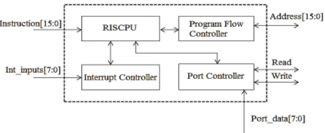
The reduced instruction set interrupt controller (RISI Controller) architecture mainly consists of ALU (Arithmetic and logical Unit), Port Controller, Interrupt controller and Register Array and its block diagram is shown in the Fig. 1. It contains RISCPU, Interrupt controller, Port controller and Program flow controller. These blocks are connected by internal buses.
Figure 1. Block diagram of a RISI Controller
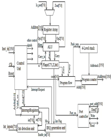
Figure 2.Internal architecture of RISI CONTROLLER
The instruction length of RISI Controller is 16-bit wide.RISI Controller has three flags namely carry, zero and interrupt flags. Both zero and carry flags are affected only during the execution of arithmetic and logical instructions and these are also useful for determine the flow of execution when branch and jump instructions take place. CPU checks the interrupt flag after completion of every instruction to know whether interrupt is available or not.ALU is capable of performing the Arithmetic (Like Addition and subtraction) and Logical operations (like And, Or, Xor and Cmpl). There are no special purpose registers in the CPU like accumulator and there is no priority among them.
RISI Controller has multi read port and single write port. Generally read operations are performing during the positive edge of the clock and write operation is performing during negative edge of the clock. Stack is used to store up to four addresses during interrupt and Branch related instructions. Port controllers take care of the read and write operation. An 8-bit address value provided on the PORT bus together with a READ or WRITE strobe signal indicates the accessed port. The port address is either supplied in the program as an absolute value or specified indirectly as the contents of any of the eight registers
There are some specific instructions useful for the controlling of interrupt controller present in the RISI CONTROLLER.
provide by CPU. Interrupt controller are used to increase the number of interrupt inputs available to CPU. The block diagram, of interrupt controller is shown in figure3.
Figure3.Block diagram of Interrupt Controller
Interrupt controller composed with three blocks. They are Interrupt Register block, Edge interrupt detection unit and Interruptrequest generation unit. Interrupts are identified by interrupt detection unit during the negative clock edge of the clock. Whenever interrupts are detected, check for the corresponding interrupt input masked or not. Unmasked interrupt input set the corresponding bit in the interrupt status register. IRQ generation unit generates the interrupt request by using the IVR contents. Interrupt request reaches the CPU send an acknowledgement signal.
Int_inputs are used to monitor the interrupts coming from various peripherals or external devices. Each interrupt register has a unique address and identified by using Addr input. To write the contents of Data input into the interrupt registers require a high valid_wr input. Intr flag input indicates the status of interrupt flag present in the CPU.
Interrupt Detection Unit detects the interrupts coming from peripheral or external devices and actives the logic to generate enable interrupt to controller. It monitors the interrupt inputs composed of interrupt signal coming from external devices or peripherals and rises enabled interrupts according to arrival signals, Interrupt Request (IRQ) Generation unit contains the Generation logic of the Interrupts towards the processor.Interrupt requests generation is also configurable as either a pulse output for an edge sensitive request or as a level output that is cleared when the interrupt is acknowledged. Interrupt Registers handles the interrupt priorities, deciding which, interrupts are enabled or disabled and managing of interrupt acknowledgements. It contains the following Registers
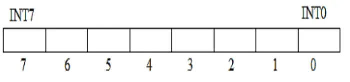
Figure 4. Interrupt Status Register
Interrupt Pending Register (IPR) gives the information about the interrupts that are both active and enabled. By default all the bits in IPR are set to zero. Any bit set to „1‟ indicates that the corresponding interrupt is waiting for processing and „0‟ indicate no interrupt isavailable. The IPR is shown in the figure 5
Figure 5. Interrupt Pending Register
Interrupt Enable register (IER) keeps track which interrupts are allowed to be handled. Writing a „1‟ to a bit in this register enable the corresponding interrupt input signal. Writing a „0‟ to a bit disable or mask the corresponding interrupt input signal
Interrupt Acknowledge Register (IAR)is used to disabling the interrupt request with selected interrupt input. Writing a „1‟ to a bit location will clear the interrupt request that was generated by the corresponding interrupt input and Writing „0‟ does nothing. The IAR is shown in the figure 6
Figure 6. Interrupt Acknowledge Register
Interrupt Vector Register (IVR) contains the ordinal value of the highest priority, enabled, active interrupt input. INT0 (always the LSB)is the highest priority interrupt inputand each successive input to the left has a correspondingly lower interrupt priority. If no interrupt inputs are active then the IVR will contain all ones. The Interrupt Vector Register (IVR) is shown in the figure 7.
Figure 7.Interrupt Vector Register
Master Enable Register (MER) is used to enabling the interrupt requests to the processor. Writing a „1‟ to ME bit enables the IRQ output signal and „0‟ to ME bit disable the IRQ output signal in other words masking all the interrupt inputs. The Master Enable Register (MER) is shown in the figure 8.
Figure 8.Master Enable Register
The following are the important features of Interrupt controller present in the RISIController. They are i) Priority between interrupt requests is determined by vector position. The least Significant Bit (LSB, bit 0) has the highest priority. ii) Interrupt enable register for selectively disabling or enabling of individual interrupt inputs. iii) Master enables register for disabling interrupt request. iv) Easily cascaded to provide additional interrupt inputs. v) Low power and less area
IV. IMPLEMENTATION
The RISI CONTROLLER is implemented using Xilinx platform on Virtex4 FPGA Family in VerilogHDL. The flowchart for the Interrupt controller is shown in the figure 9. Application specific instructions [13] were designed for controlling the interrupt controller along with general purpose instruction set.
By using Application specific instructions [13] processor can perform several operations on interrupt controller. The operations like masking or unmasking of interrupts disable interrupt request for the execution of important instructions. Interrupt controller uses fixed priority algorithm for generating the interrupt request.
The MER must be programmed based on the intended use of the Interrupt Controller.There are two bits in the MER: the Hardware Interrupt Enable (HIE) and the Master IRQ Enable (ME). The ME bit must be set to enable the interrupt request output.Check whether the Msb bit (ME) in MER register is set or not. If ME bit in the MER register is not set the interrupt requests are not generated. Check the status of the interrupt flag. If the flag bit is set Interrupt request is generated and wait for acknowledgement which is coming from the processor. Next interrupt request is generated only when the acknowledgement is received otherwise; wait until the acknowledgement is received.
By the execution of the following code the RISI Controller disables the interrupt request and enables it again after some time. The simulation results regarding the execution of the program1 are shown in the results section
Program 1
MID 00 --- Disables the interrupt Request MOV R4, 5F --- Load the immediate data5F into register R4 MOV R5, 5F --- Load the immediate data 5F into register R5 ADD R4, R5 ---Add the contents of R5with R4 and result is Stored in R4
MIE 80 --- Enables the interruptrequest
RISIController is capable to handle 8 interrupt inputs at a time. Interrupt controller uses positive clock cycle for interrupt request generation whereas negative clock cycle used for receiving an interrupt Acknowledgement which is coming from CPU.
V. RESULTS
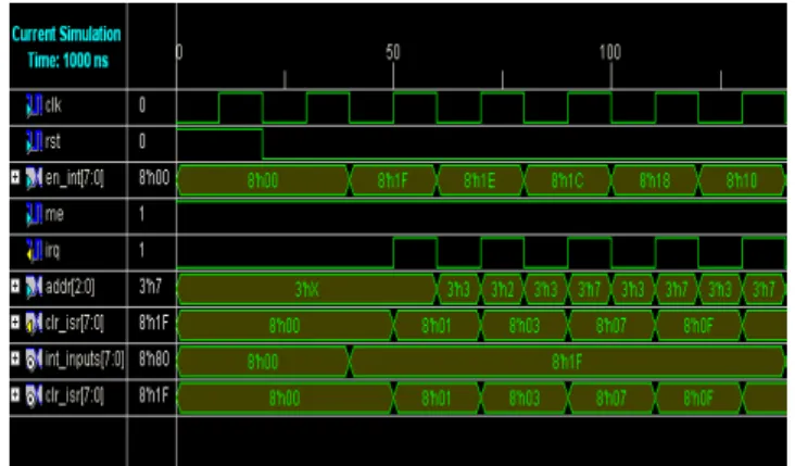
All the modules of RISI CONTROLLER are simulated and verified using the Xilinx tools. The simulation result of Interrupt controller shown in figure 10. When the reset is high all the register present in the interrupt controller are loaded with default values. Interrupts are identified during the negative edge of the clock signal. The content of IER indicates whether the interrupts are mask or unmask. En_int is obtained by anding the content of IER with Int_inputs.
Each register present in the interrupt controller have a unique address. Registers are identified by using addr input. The content ofEn_int is also stored in the ISR. Interrupt request is generated only if both the ME and Intr flag arehigh. Priority between the interrupts is generated by using the fixed priority scheme. The contents of Clr_isr are set at the time of interrupt request generation
.
Top level timing diagram between interrupt controller and RISCPU is shown in figure 11. Whenever the CPU receives interrupt request, wait for the completion of current instruction and store the address of next instruction in the stack. Load the contents of program counter with address FF and send an
Figure 10.Top level timing diagram of Interrupt Controller
Status of intr flag is changed from high to low when the interrupt request is received. CPU does not receive any interrupt even though Int_inputs are active because Me output is low indicate that interrupt request is disabled. The status of
Meoutput is high then only the CPU receives the interrupt request and it is shown in the figure 11.
Figure 11: Top level timing Diagram between the Interrupt controller and RIS CPU
The top level module with input and out signals of the RISI Controller and Interrupt Controller is shown in figures 12, 13 and the RTL schematic of the Interrupt Controller is shown in the figure 14.
Figure 13. Signals of Interrupt Controller(IC)
The RTL schematic of the Interrupt Controller of RISI Controller is shown in figure 14. The Interrupt controller consists of a Register block, edge interrupt detection unit and IRQ generation unit. Interconnection between the blocks and the input output signals of the Interrupt Controller module are also shown in the figure 14.
Figure 14.RTL Schematic of Interrupt controller of RISI Controller
Figures 15 and 16 represents the layout of the RISI Controller and Interrupt controller implemented onto the Vertex4 FPGA family. In the Fig. 15 and 16 the colored area represents the components of the RISI CONTROLLER that are placed on the FPGA and the place and routed diagrams of the Interrupt Controller are shown in figures 17 and 18 respectively
Figure 15. RISI Controller Layout on FPGA
Placement involves deciding where to place all electronic components, circuitry, and logic elements in limited amount of space. This is followed by routing, which decides the exact design of all the wires needed to connect the placed components.
Figure 16.Interrupt controller(IC) layout on FPGA
This must implement all the desired connections by following the rules and limitations .The complete placed and routed diagram of the RISI Controller is shown in figure 17.
Figure 17.Place and Route diagram of RISI CONTROLLER
The place and route diagram of theInterrupt controllerof RISI Controller is shown in figure 18.
Figure 18. Place and Route diagram of Interrupt Controller(IC)
In the Table I the comparison of different parameters related to the area of RISI Controller and Mpcore were specified. The graph clearly shows that the number of slices and LUTs utilized by the RISI Controller less than that of the Mpcore. The graph also indicates in othersense that the area occupied by RISI Controller on the FPGA is less.
TABLE I.COMPARISON OF DEVICE UTILIZATION PARAMETERS OF MPCORE AND RISICONTROLLER
Parameter Mpcore RISI
CONTROLLER Number of slice
Registers
349 318
Slices containing related logic
496 467
Figure 19.Comparison of delay parameters for Mpcore and RISI Controller
Power is one of the main constrain in the design of controller. Clock signal [4] contribute major power consumption source. To reduce the clock power dissipationclock gating techniques are employed. The power consumption of the RISI CONTROLLER was described in the figures 20 and 21. The figures also give us a comparative view of the power consumption of the Mpcore and RISI CONTROLLER cores.
In the figure 21 the deviation of the curves indicate that the operating voltage increases the power consumption of the Mpcore increases more rapidly when compared with designed controller power. Similarly figure 20 describes the variation of power with respect to frequency for the Mpcore and RISI CONTROLLER.
Figure 20. Power consumption of RISI CONTROLLER at 1.2v
Figure 21.Plot b/w Voltage and Power of Mpcore and RISI Controller at 1 GHz
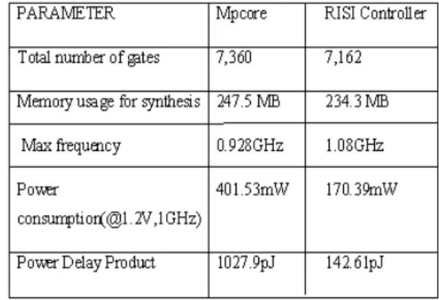
The Power-delay product is simply the product of the power consumption and the time delay. The smaller value of the power-delay product, performance of the design is better. Since this RISI CONTROLLER has almost negligible power-delay product value, it indeed has a better performance in terms of the speed and power dissipation.
TABLE II.COMPARISON OF MPCORE AND RISICONTROLLER
Table II shows the comparison of different parameters related to the Mpcore and RISI CONTROLLER; it has better performance than the Mpcore.
VI. CONCLUSION
REFERENCES
[1] A. Tumeo, M. Branca, L. Camerini, M. Monchiero,G. Palermo,F. Ferrandi and D. Sciuto, “An Interrupt Controller for FPGA-based Multiprocessors”, International Conference on Embedded Computer Systems: Architures, Modeling and Simulation, July 2007,pp. 82-87. [2] Wei Chipni, Li Ahao lin, Zheng Qingwei,Ye Jianfei, and Li Shenglong,
“Design of a configurable multichannel interrupt controller”,Second Pacific-Asia Conference on Circuits,Communications and System, vol. 1,Aug 2010, pp. 327–330.
[3] Pizhou Ye,and Chaodong Ling, “A RISC CPU IP core”,Second International Conference on Anti-counterfeiting,Security and Identificatiom ,August(2008), pp. 356–359,2008.
[4] H. Jacobson,P. Bose, Zhigang Hu,A. Buyuktosunoglu, V.Zyuban,R. Eickemeyer,L. Eisen,J. Griswell,D. Logan,Balaram Sinharoy, and J. Tendler,“ Strenching the limits of clock-gating efficiency in server-class processors”,Eleventh International Symposium on High-performance Computer Architecture,Feburary (2005), pp . 238- 242,2005.
[5] Xiaotao Chang, Mingming Zhang, Ge Zhang, Zhimni Zhang and Jim Wang,“Adaptive Clock Gating Technique for Low Power IP Core in SoC Design”,IEEE International Symposium on Circuits And Systems,May(2007),pp. 2120 – 2123, 2007..
[6] S. Ghosh, D. Mohapatra, G. Karakonstantis and K. Roy,“ Voltage Scalable High-speed Robust Hybrid Artihmetic Units Using Adative Clocking”IEEE Transactions on Very Large Scale Integration Systems,September(2010),Vol. 18, pp.1301- 1309,2010.
[7] Hai Li, S. Bhunia,Y. Chen,T.N. Vijaykumar and K.Roy,“ Deterministic clock gating for microprocessor power reduction”, Ninth International Sympossium on High-Performance Computer Architecture, February (2003), pp. 113 – 122, 2003.
[8] E. Ozer, S.W. Sathaye, K.N. Menezes, S. Banerjia, M.D. Jenningsand T.m. Conte,“ A fast interrupt handling scheme for VLIW processors”,International Conference on Parallel Architecures and Compilation Techniques,October(1998),pp. 136 -141 ,1998.
[9] G. Kane and J. Heinrich,“ MIPS RISC Architecture: reference for the R2000,R3000,R6000 and the new R4000 Instruction set computer Architecture”, Prentice-Hall,Englewood Cliffs,NJ,1992.
[10] Krall. A, “ An extended Prolog instruction set for RISC processors” in VLSI for Artifical Intelligence and Neural Networks,J.G. Delgado-Frias and W.R. Moore, Eds-Plenum Press, New York,pp. 101-108,1991. [11] Motorola Inc.“M6800 8/16/32- Bit MICROPROCESSOR”,avilable
athttp://www.freescale.com/files/32bit/doc/ref_manual/MC68000UM.pd f
[12] J. Rose,A.E. Gamaland A. Sangiovanni and A. Vincentelli,“ Architecture of Field-Programmable Gate Arrays”, Proc. IEEE,Vol81,no 7,July,pp. 1013-1020,1993.
[13] J. Vanprate, Gossens .G, D. Lanner, and H. De man,“ Instruction set definition and insstruction set selection”,in Proc. Of seventh International Symposium on High-Level Synthesis,pp. 11- 16,1994. [14] ARM11 Mpcore available athttp://www.arm.com.
[15] IBM. Multiprocessor Interrupt Controller Data Book,March,2006. [16] Xilinx OPB Interrupt Controller (v1.00c),January 2005.
[17] A. De Gloria,Paolo Faraboschi and Mauro Olivieri,“ A Self TimedInterrupt Controller: ACase study in Asynchronous Micro_Architecture Design ” Seventh Annual IEEE International ASIC Conference and Exhibit ,pp. 296 – 299,1994.
[18] G. Palumbo,F. Pappalardo,and S. Sannella “ Evaluation on power reduction applying gated clok approes”,IEEE International Symposium on Circuita and Systems,Vol.4,pp.IV-85-IV-88,2002.
[19] Nakasimha .K,S. Kusakabe,H. Taniguchi,and M. Amamiya “ Design and implementaion of Interrupt packaging mechanisum”,International Workshop on Innovative Architecture for Future Generation High-performance processors and systems”, pp. 95-102,2002
[20] J.E. Smith, and A.R. Pleszkun,“ Implementing Precise Interrupts in Pipelined Processors” IEEE Trans. On Comp.,Vol.37,pp. 291-299,1975. [21] Horelick Dale “ simple Versatile Camac Crate Controller and Interrupt
Priority Encoding Module ”, IEEE Transaction on Nuclear Science,Vol. 22,pp. 517- 520,1975.
[22] Qiurong Wang “ An Interrupt Management Scheme Based on Application in Embedded system”,Multimedia and Informetion Technology,pp. 449-452,2008.