R.Prabakaran Int. Journal of Engineering Research and Applications
www.ijera.com
ISSN : 2248-9622, Vol. 5, Issue 5, ( Part -3) May 2015, pp.61-66
Reducing Area & Power Overhead In Design of Light Weight
Sensor For Detection of Reclcled ICS
1#
R.Prabakaran,
2#B.Prabhakaran
PG Student [VLSI], Dept. of ECE, Maha Barathi Engineering College, Chinnasalem, Tamil Nadu, India1 Assistant Professor, Dept. of ECE, Maha Barathi Engineering College, Chinnasalem, Tamil Nadu, India2
Abstract
The counterfeiting and recycling of integrated circuits (ICs) have become major issues in recent years, potentially impacting the security and reliability of electronic systems bound for military, financial, or other critical applications. With identical functionality and packaging, it would be extremely difficult to distinguish recycled ICs from unused ICs. In the existing Ring Oscillator (RO) based sensor with 90nm technology test chip shows the effective detection of recycled ICs. The impact of RO based sensor is that, it is difficult to identify recycled ICs used shorter than one month and it requires more power and area overhead. To provide a solution to the existing system, Clock Anti fuses (CAF) based sensor is implemented to enhance the effective recognition of recycled ICs even if the IC used for a very short period. MAF is implemented in FPGA to verify its effectiveness.
Keywords
: Counterfeiting; Hardware security; MAF;Recycled ICs.I.
INTRODUCTION
The counterfeiting of integrated circuits (ICs) is on the rise, potentially impacting the security of a wide variety of electronic systems. A counterfeit component is depend as an electronic part that is not genuine because it.
1) Is an unauthorized copy.
2) It does not conform to original component manufacturers design, model, or performance. 3) It has incorrect or false markings and
documentation.
3) Is not produced by the original component manufacturers or is produced by unauthorized contractors.
4) Is an off-specification, defective, or used original component manufacturers product sold as new or working. In this paper, the term recycled ICs is used to denote used ICs being sold as new or remarked as higher grades. The terms unused ICs and new ICs represent the ICs that are brand new. On the other hand, most ICs used in the meld are not turned on all the time. Consider an IC used in a cell phone, for example; the cell phone may only be powered on during the day for some period. The real (power-on) usage time of the IC would be much shorter than the usage time with power-off intervals. In this paper, the term usage time is used to represent the accumulated power-on time even if the IC is used intermittently.
In general, the recycled ICs have the original appearance, functionality, and markings as the devices they are meant to mimic, but they are used for a period before they are resold. Even the best
visual inspection techniques will have difficulty in identifying these ICs with certainty.
II.
RELATED WORK
Suh Getal [1] proposed PUF for device authentication and secret key generation .The proposed PUF design with exploit inherent delay characteristics of wires and transistors that differ from chip to chip and describe how PUFs can enable low cost authentication of individual ICs and generate volatile secret keys for cryptographic operations. A common ingredient that is required to enable the security operations in an IC is a secret on each IC, which an adversary cannot obtain or duplicate.
Hori. Y et al[3] observed that most of the PUF's aging instability happens early in its lifetime. Due to the typical differential nature of PUF structures, stability does not change significantly with age. Further, a high correlation has been observed between instability that is caused due to aging and instability that is caused due to temperature. In various RO-PUF setups and operating conditions that around 4% of the PUF bits are prone to instability
due to aging Silicon Physical
Unclonable Functions (PUF) are novel circuits that exploit the random variations that exist in CMOS manufacturing process to generate chip-unique random bits. Aging is primarily due to phenomena like Bias Temperature Instability (BTI) and Hot Carrier Injection (HCI).
Kim Tet al [4] proposed a silicon odometer which is an on-chip reliability monitor for measuring frequency degradation of digital circuits. A Precise
R.Prabakaran Int. Journal of Engineering Research and Applications
www.ijera.com
ISSN : 2248-9622, Vol. 5, Issue 5, ( Part -3) May 2015, pp.61-66
measurement of digital circuit degradation is the key aspect of aging tolerant digital circuit design. They presented a fully digital on chip reliability monitor for high-resolution frequency degradation measurements of digital circuits. It measured the beat frequency of two ring oscillators, one stressed and the other unstressed, to achieve 50 higher delay sensing resolution than that of prior techniques.
Roy Jet al [5] proposed a novel comprehensive technique to End Piracy of Integrated Circuits (EPIC). It requires that every chip be activated with an external key, which can only be generated by the holder of IP rights, and cannot be duplicated. EPIC is based on (i) automatically generated chip IDs, (ii) a novel combinational locking algorithm, and (iii) innovative use of public key cryptography. Major required components have already been integrated into several chips in production.
Tyagi Aet al [6] came up with the idea of reconfigurable logic barriers for preventing IC piracy. This is a hardware metering technique that prevents duplicating of an IC. Hardware metering, or IC metering refers to mechanisms /protocols that enable tracking of the ICs post fabrication
III.
EXISTING SYSTEM
3.1 COUNTERFEIT DETECTION METHODSA specialized service of testing has been created for detecting counterfeit components.Counterfeit components have similar external appearance, functions and specifications as the devices.
3.2 PHYSICAL INSPECTIONS
Physical inspections are based on the physical properties of the component. Physical inspections are the first set of tests, to be performed on the incoming components for authentication .Physical inspections tests is broadly classified into four categories.
i. Incoming Inspection ii. Exterior Tests
iii. Interior Tests iv. Material Analysis
3.2.1 Incoming Inspection
In incoming inspection, all the components were inspected thoroughly. The external structure is observed carefully by low-power visual inspection (LPVI) while the internal structure is inspected by X-ray imaging.
Low-Power Visual Inspection (LPVI): LPVI is the first test usually performed on all the components. The leg and packages are carefully examined using a low-power microscope or magnification lamp, generally with less than 10Xmagnification
3.2.2 Exterior tests
Micro blast Analysis: Micro blasting is a dry blasting counterfeit technique in which accurately defined blasting agents are bombarded on the surface of the target device, in an effort to remove part markings and scratches from recycled and used parts or falsely represent new parts (e.g. upgrading temperature or speed-grade). Compressed air is generally used to accelerate the blasting particles. Some popular blasting agents, such as aluminium oxide powder, sodium bicarbonate powder, and glass bead, are used, depending on the components, package type.
2.2.3 Material analysis
Internal chemical composition of the IC is analyzed using material analysis. This is the only tests that can identify defects and abnormalities related to materials. There are many tests available that can perform material analysis such as X-ray fluorescence (XRF), Fourier Transform Infrared Spectroscopy (FTIR), RAMAN Spectroscopy etc.
Fourier Transform Infrared (FTIR) Spectroscopy: FTIR works based on infrared (IR) spectroscopy. A part of IR radiation is absorbed by the material under test and the other part is transmitted through it. The spectrum for molecular absorption and transmission is observed from the resultant IR radiation.
FTIR is used to authenticate both organic and inorganic materials of a component. It is used to verify
i. polymer, coating of the package
ii. Residual foreign materials from the sand blasting process used to remove the old markings.
3.3ELECTRICAL TESTS
These methods are mostly used to verify the correct functionality and performance of ICs.
R.Prabakaran Int. Journal of Engineering Research and Applications
www.ijera.com
ISSN : 2248-9622, Vol. 5, Issue 5, ( Part -3) May 2015, pp.61-66
Parametric tests are performed to measure the AC/DC parameters of the chip. In DC parametric test, it measures the electrical parameters using ohm‟s law. These tests include contact test, power consumption test, output short current/drive current test and threshold test.
3.3.2 Functional Tests
In functional verification component‟s
functionality is verified and most of the defects can be detected by these tests. It is one of the most efficient and expensive way of detecting IC counterfeits. For a memory device, read/write operations can be performed to verify its functionality e.g. MARCH tests.
3.3.3 Burn-In Test
Burn-In test is an accepted practice for detecting early failures in a population of semiconductor devices. The device is operated at an elevated temperature to determine infant mortality failures and unexpected failures in order to ensure reliability. This process may also be called heat soaking. Components may be under continuous test or simply tested at the end of the burn-in period.
3.4 AGING-BASED STATISTICAL
FINGERPRINT
During the lifetime of an IC, performances continuously degrade due to aging mechanisms. Using recycled counterfeit ICs as brand new will significantly reduce the capability of a device to perform its required functions for prolonged period of time. The most common aging phenomena include electro-migration, negative bias temperature instability (NBTI), hot carrier injection (HCI), and time-dependent dielectric breakdown (TDDB).
The following two methods leverage the impact of these aging phenomena in order to detect recycled counterfeit ICs.
3.4.1 Early Failure Rate (EFR) Data Analysis The measurements used to build the classifier are typical test results from production early failure rate (EFR) analysis required to release most products, such as Vmin, Fmax, and Iddq, thus no additional costs are incurred to perform identification. A low cost statistical approach is to detect recycled counterfeit ICs by training a one-class classifier using only brand new devices.
3.4.2 Circuit Path-Delay Analysis
A path-delay finger printing technique, which was first introduced in the context of hardware Trojan detection, is adapted to distinguish recycled ICs from new ones. Due to degradation in the field, the path-delay distribution of recycled ICs will become different from that found in new ICs.
Statistical data analysis can effectively separate the impact of process variations from aging effects on path delay.
3.5 PUF
PUFs can enable low cost authentication of individual ICs and generate volatile secret keys for cryptographic operations. A common ingredient that is required to enable the security operations in an IC is a secret on each IC, which an adversary cannot obtain or duplicate. PUFs significantly increased physical security by generating volatile secrets that only exist in a digital form when a chip is powered on and running.
A physical random function or physical unable function is a function that maps a set of challenges to a set of responses based on an intractably complex physical system. The function can only be evaluated with the physical system, and is unique for each physical instance. PUFs can be implemented with various physical systems. Even with identical layout masks, the variations in the manufacturing process cause significant delay differences among different ICs.
An advantage of PUFs is that they do not require any special manufacturing process or programming and testing steps. The disadvantage is that it only authenticates the integrated circuits, not detect the recycled ICs.
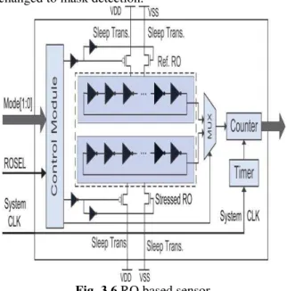
3.6 RO BASED SENSOR
The RO-based sensor is composed of a reference RO and a stressed RO. The stressed RO is designed to age at every high rate using high threshold voltage (HVT) gates to expedite aging hence ICs used for a period can be identified. The reference RO is gated off from the power supply during chip operation, hence it experiences less stress.
The frequency difference between the two ROs could denote the usage time of the chip under test (CUT); the larger the difference is, the longer the CUT is used, and with a higher probability the CUT could be a recycled IC.
With close placement of the two ROs in the RO-based sensor, the impact of inter die process variations could be minimized. Data analysis can effectively distinguish the frequency differences caused by aging from those caused by temperature and inter die process variations, to identify recycled ICs, which is demonstrated by our simulation and silicon results.
The RO-based sensor presents a negligible area overhead, imposes no constraint on circuit layout, and is resilient to removal and tampering attacks.
R.Prabakaran Int. Journal of Engineering Research and Applications
www.ijera.com
ISSN : 2248-9622, Vol. 5, Issue 5, ( Part -3) May 2015, pp.61-66
frequency difference between the two ROs cannot be changed to mask detection.
Fig. 3.6 RO based sensor
The structure of our RO-based sensor is shown in fig 2.2, which is composed of a control module, a reference RO, a stressed RO, a MUX, a timer, and a counter. The counter measures the cycle count of the two ROs during a pre-specified time, which is controlled by the timer. System clock is used in the timer to minimize the measurement period variations because of circuit aging.
3.7 LIMITATIONS
i. In the RO-based sensor still be difficult to completely exclude the impact of intertie process variations on the sensor.
ii. In addition, RO based sensor provides only an approximation of the usage time
iii. The sensitivity (the minimum usage time of recycled ICs detected by sensors) of the RO-based sensor is limited.
iv. The RO based sensor is difficult to identify recycled ICs.
v. It requires more power
IV.
PROPOSED SYSTEM
4.1 ANTIFUSE BASED SENSOR LOGIC CIRCUIT
The AF-based sensor composed of counters, adder, data module and memory block. The counters are used to record the usage time of ICs and the value is dynamically stored in the AF memory block. As the AF memory block is one-time programmable (OTP), recyclers could not erase the context during recycling process.
4.2 ANTIFUSE MEMORY
The typical interface of the embedded AF memory is shown in Fig.3.2 consists of power supply, address and data signals.
Fig. 4.2 Typical Interface of Anti fuses Memory
The features of AF block in the AF-based sensor are as follows:
i. It consumes less power to program or read compared with other types of OTP structures, such as electrical fuse or CMOS floating gate. ii. The area of an AF is much smaller than anti
fuse
iii. It does not require additional mask
Most AF memories are programmed in a programming environment with relatively high voltage/current. Therefore, integrated charge pumps or voltage multipliers are used to provide sufficiently high voltage/current in embedded AF OTP memories. With those charge pumps or voltage multipliers, no additional power supply is required during programming.
4.3 TYPES OF ANTIFUSE BASED SENSOR STRUCTURES
Two different structures of AF-based sensor are proposed to measure the usage time of ICs.
i. Clock anti fuse (CAF) sensor ii. Signal anti fuse ( SAF) sensor
4.3.1 Clock Anti fuse (CAF) Sensor
AF-based sensor using clock AF (CAF) records the cycle count of the system clock during the chip operation. The usage time of recycled ICs can be reported by this sensor and the measurement scale and total measurement time could be adjusted according to the application of ICs.
4.3.2 Signal Anti fuse (SAF) Sensor
R.Prabakaran Int. Journal of Engineering Research and Applications
www.ijera.com
ISSN : 2248-9622, Vol. 5, Issue 5, ( Part -3) May 2015, pp.61-66
4.4 CAF SENSOR STRUCTURE
The structure of the CAF-based sensor, which is composed of two counters, a data read module, an adder, and an AF OTP memory block. Sys clock in the Fig.3.3 is the high-frequency system clock, providing clock for different modules including the data read module, the AF block, and registers Counter1 is used to divide the high- frequency system clock to a lower frequency signal. Counter2 is used to measure the cycle count the lower frequency signal.
The size of the two counter scan be adjusted accordingly depending on the measurement scale. As the data stored in registers (counters) could be lost or reset when power supply is off, no erasable memory is required in this sensor.
Fig.4.4 Structure of the CAF-based sensor.
An embedded AF OTP block is used instead of a field-programmable read-only memory (FPROM) to store the usage time information because FPROM could be tampered or altered by attackers.
In the AF block, program is assigned to be 1_b1 if the value in counter2 increases by 1.Through connecting the output of counter2 to address in the AF block directly, the related AF cell will be programmed as 1.Therefore, the largest address of the cell whose content is 1 will be the usage time of CUT based on the measurement scale setup by counter1
Program and read operations, share the same address signals in AF block. Therefore, a MUX1 is controlled by data read module, is used to select the address (AF cell) to be read or programmed. Every time power supply is on, the AF block will work in read mode for a short period. During this time, the read address generated by data read module will go through MUX1 and all the AF cells will be traversed based on the traversing binary tree principle.
The reason for using an adder is that, counters start from 0 every time the power is turned on and the previous usage time must be considered when it calculates the total usage time. In addition, Reg1 is
used to sample the data in adder, Reg2 delays the data in Reg1with one system clock, and XOR gates are used to compare the data in Reg1 and Reg2.
If they are different (denoting the usage time increased), the AF OTP block will work in program mode and the data in Reg1 will go through MUX1 to the address in the AF block. Therefore, combined with the value incounter2 (the usage time after power-on), the new total usage time will be stored in the AF OTP block by programming anew AF cell with a larger address
To eliminate the need for additional pins for authentication purposes on the chip, CAF-based sensor uses a MUX2 and an authentication (Auth) pin to send the usage time to the output pins of ICs. Thus, no extra output pins will be added to the original design.
i. When the IC works in normal functional mode, original primary outputs will go through MUX2.
ii. If the IC is in authentication mode by enabling the authentication signal, the data read module will set the AF IP in read mode and the usage time will go through MUX2.
POWER ANALYSIS
The power analysis of CAF is respectively to evaluate the power consumption. The system clock of 24MHz is considered for this evaluation It is obtained from the table 4.4 the proposed CAF consume less clock power of 0.0034W. It is obtained from the table 4.3 the proposed CAF consume power of 0.030W in Spartan 3E.
Total IO power analysis of CAF in Spartan 3E
V.
CONCLUSION
R.Prabakaran Int. Journal of Engineering Research and Applications
www.ijera.com
ISSN : 2248-9622, Vol. 5, Issue 5, ( Part -3) May 2015, pp.61-66
breaking the chip. The power utilized in the sensors can be reduced by implementing clock gating logic. This technique reduces switching activity in the system as well as time required. Experimental results and analysis confirmed the effectiveness of the CAF sensor to detect the recycled ICs.
REFERENCES
[1] G. Suh and S. Devadas, “Physical unclonable functions for device authentication and secret key generation”, inProceedings of 44th ACM/IEEE Design Automation. Conference. pp. 9–14,Jun. 2007.
[2] E. Ozturk, G. Hammouri, and B. Sunar, “Physical unclonable function with tristate buffers”, in Proceedings. IEEE International. Symposium. Circuits System., pp. 3194– 3197,May 2008.
[3] Y. Hori, T. Yoshida, T. Katashita, and A. Satoh, “Quantitative and Statistical Performance Evaluation of Arbiter Physical Unclonable Functions on FPGAs”, in International Conference on Reconfigurable Computing and FPGAs, pp.298–303, 2010. [4] T. Kim, R. Persaud, and C. H. Kim, “Silicon
odometer: An on chip reliability monitor for measuring frequency degradation of digital circuits”, IEEE J. Solid-State Circuits, vol. 43, no. 4, pp. 974–880,Apr. 2008.
[5] J. Roy, F. Koushanfar, and I. Markov, “EPIC: Ending piracy of integrated Circuits”, Proceedings of Conference. Design, Automation. Test, pp. 1069– 1074,2008.
[6] A. Baumgarten, A. Tyagi, and J. Zambreno, “Preventing IC piracy using reconfigurable logic barriers”, IEEE Design Test Computation., vol. 27, no. 1, pp. 66– 75,Jan.–Feb. 2010.
[7] J. Keane, X. Wang, D. Persaud, and C. H. Kim, “An all-in-one silicon odometer for separately monitoring HCI, BTI, and TDDB”, IEEE J. Solid-State Circuits, vol. 45, no. 4, pp. 817–829,Apr. 2010.
[8] Xiaoxiao Wang, Dat Tran, Saji George, Le Roy Winem berg, Nisar Ahmed, Radic “ A Standard-Cell-Based Sensor for On-Chip Aging and Flip-Flop metastability Measurements”, Proceedings of IEEE International conference, vol.24, no.1,pp.65-74, 2012.
[9] K. Huang, J. Carulli, and Y. Makris, „„Parametric counterfeit IC detectionvia support vector machines‟‟, in Proeedings of IEEE International. Symposium. Defect Fault ToleranceVLSI Nanotechnology. System.,pp. 7–12,2012.
[10] U.Guin, D.DiMase, and M. Tehranipoor, „„A comprehensive framework for counter feitdefect coverage analysis and detection assessment‟‟, Journal of Electron. Testing, vol. 30, no. 1,pp. 25–40, 2014.
[11] X. Zhang and M. Tehranipoor, “Identification of recovered ICs using fingerprints from a light-weight on-chipsensor”, in Proceedings of Design Automation. Conference, pp. 703–708, 2012.