JOURNAL OF NANO- AND ELECTRONIC PHYSICS Р А А - А Р
Vol. 5 No 4, 04021(3pp) (2013) Том5№ 4, 04021(3cc) (2013)
The article was reported at the International Conference «Physics and Technology of Nanomaterials and Structures», Kursk, 21-22 November, 2013
2077-6772/2013/5(4)04021(3) 04021-1 2013 Sumy State University
Short Communication
Some Aspects of Phosphorus Diffusion in Germanium in In0,01Ga0,99As / In0,56Ga0,44P / Ge Heterostructures
S.P. Kobeleva*, I.M. Anfimov, S.Y. Yurchuk, A.V. Turutin
National University of Science and Technology “MISIS”, Department of New Materials and Nanotecnology, 4, Leninsky Pr., 119049 Moscow, Russia
(Received 05 August 2013; revised manuscript received 05 November 2013; published online 10 December 2013)
The results of experimental and theoretical researches of phosphorus distribution in the first cascade of a multi cascade solar cell based on nanoscale structures AIIIBV / Ge are presented. Secondary ion mass spec-troscopy has been applied to obtain profiles of phosphorus and gallium in In0.01Ga0.99As / In0.56Ga0.44P / Ge het-erostructure. In the germanium surface there is a thin layer of about 26 nm, in which the gallium concentra-tion exceeds the concentraconcentra-tion of phosphorus. Therefore a nanoscale p-n junction forms that does not have a significant impact on the solar cells performance at room temperature. Phosphorus diffusion is much slower in this area than in area with electronic conductivity. The main p-n junction is formed at a distance of 130-150 nm from the surface of the germanium. Diffusivity of gallium (DGa 1,410– 15 cm2/s) is markedly higher than described in a literature. Diffusivity of P increase from DP 310-15 cm2/s on the boundary of the hetero-structure In0, 49Ga0, 51P to DP 5,210– 14 cm2/s in n-type Ge.
Keywords: Multi cascade solar cell, Diffussion of P in Ge, Diffusion of Ga in Ge, Heterostructure.
PACS number: 66.30.h
1. INTRODUCTION
During the last decade Ge has received renewed at-tention as a potential material for nanoscale electronic. In particular the best multi cascade A3B5 solar cells are produced on the Ge substrate and transformation of the infrared part of solar energy to electric power is performed by Ge subelement [1-2]. p-n junction in the wide-gap semiconductor materials of multi cascade solar cells is produced during epitaxial growth, while phosphorus diffusion is used for the creation of the p-n junction in germanium subelement. The optimization of the p-n junction depth requires accurate dopant dif-fusion modeling in germanium. However, the current knowledge on dopant behavior in Ge is still rather poor as compared to that of Si. Although recent experi-mental data appear in complement to the earlier (40 years old) ones, the underlying physical mecha-nisms are not fully understood [3-9]. A vacancy-assisted mechanisms generally accepted, but details such as exact charge state of the defects, the roles of the simple exchange mechanism, or PV pair diffusion mechanism, are not clear. Experiments on the intrinsic (P concentration less than the intrinsic carrier concen-tration at the diffusion temperature) and extrinsic dif-fusion of the n-type dopants in Ge demonstrate an en-hanced diffusion of these dopants with increasing dop-ing level [5-8]. The ratio between the intrinsic Din and extrinsic Dn diffusivities at a given temperature equals the squared [5] or cubic [7] ratio between the free elec-tron concentration n and the intrinsic carrier concen-tration nin. The diffusion model that describes these tendencies is based on the proposal of constant vacancy concentration and dominant role of V-P charged pairs
in the diffusion [10]. Some experiments on co-diffusion
have shown that P diffusion suppression [8, 9] demon-strates a strong dependence of diffusion process on the
presence of other impurities in Ge. To produce compara-tively shallow (less than 200 nm) p-n junction in Ge sub-element, P diffusion should be make in heavily doped Ge. The aim of this work is to investigate the diffusion profiles of phosphorus in germanium in the In0,01Ga0,99As / In0,56Ga0,44P / Ge heterostructures.
2. EXPERIMENTAL DETAILS
The germanium p-type wafers, (100) orientation, heavily gallium doped (NGa 1018 cm– 3), were used.
The samples for the research were obtained by CVD method in the VEECO E450 LDM reactor. Three steps at T 635 C were used for Ge subelement creation: treat-ment at the phosphine flow (2.5 min), In0, 56Ga0, 44P buffer layer growth (1 min), In0,01Ga0,99As layer growth (1,6 min). Secondary ion mass spectrometry (SIMS) was carried out by PHI-6600 spectrometer for elements profiling. As it was shown previously [11] there were no significant changes in the element profiles when flux of phosphine increased from 600 to 1200 cm3/min. The main source of phosphorus in Ge substrate is In0, 56Ga0, 44P buffer layer having thickness of about 24 nm, so the diffusion time is 2,6 min [11]. Electrochemical profiling was carried out by profilometer ECV Pro.
3. RESULTS AND DISCUSSION
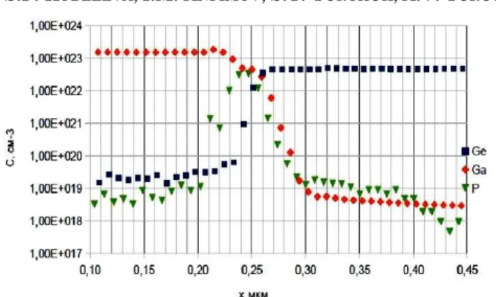
Typical profiles of elements in the examined struc-tures are shown on Fig. 1. The most surprising results are high P and Ga concentrations on the Ge surface and significant diffusion of Ga in Ge from buffer layer.
S.P. KOBELEVA,I.M. ANFIMOV,S.Y. YURCHUK,A.V. TURUTIN J.NANO-ELECTRON.PHYS. 5, 04021 (2013)
04021-2
Fig. 1 – Profiles P, Ga and Ge in the investigated structures
that does not have a significant impact on the solar cell performance at room temperature. The existence of the additional p-n junction confirmed by electrochemical profiling (Fig. 2). Phosphorus diffusion is much slower in this area than in area with electronic conductivity. The main p-n junction is formed at a distance of 130-150 nm from the surface of the germanium.
Fig. 2 – Results of electrochemical profiling of In0.01Ga0.99As / In0.56Ga0.44P / Ge heterostructure
Different diffusion mechanisms were analyzed to predict the dependence of the p-n junction depth. The p-type surface with low electron concentration leads to prediction of low diffusion coefficient Dpaccording to vacancy-assisted models [5, 7] (see Fig. 3). Using these diffusivities leads to very low P concentration. Together with high Ga concentration it leads to the inability to obtain n-type region in this structure. Experimental
phosphorus diffusivity is greater than predicted one. The comparison of the literature data and calculated Ga and P diffusivities based on the 2-nd Fikes law are shown in Table 1. Experimental and calculated profiles for two regions are shown on the fig. 4, 5. As we can see, Ga dif-fusivity is higher than the literature data [4].
In contrary to previous experimental results, phos-phorous diffusivity increase with drops of the P concen-tration. There are some reasons for observed distinc-tions. A vacancy-assisted mechanisms proposed exist-ence of the thermal equilibrium concentration of vacan-cies in Ge. Really a high Ga and P concentration in the surface area may cause changing in the vacancy distri-bution. Moreover it may lead to changing VP charge diffusion mechanism to simple exchange or interstitial one. To calculate diffusion profiles in this case we need to include generation and recombination terms to con-tinuity equation as it was done for diffusion profiles calculation in Si with taking into account kick-out mechanism [12].
Fig. 3 – Diffusivity in P SIMS profiles of P (P(1)), Ga (Ga(1)) and calculated profiles: P (P(2), DP 310– 15 cm2/s) and Ga (Ga(2), DGa 1,410– 15 cm2/s) in germanium
Table 1– The diffusion coefficients (D1015, cm2/s) in the surface area at T 635 °C
P [3] P [8] P [7] Ga [4] Ga [4] Ga P (1) P (2)
43 1,40 0,88 0,23 0,06 1,4 3,0 52
Fig. 4 – SIMS profiles of P (P(1)), Ga (Ga(1)) and calculated profiles: P (P(2), DP 310– 15 cm2/s) and Ga (Ga(2), DGa 1,410– 15 cm2/s) in germanium.
Fig. 5 – SIMS profiles of P, Ga and calculated profiles: P (DP 5,210– 14 cm2/s, P(1)-based on the second Fick's law), P (P(2) – taking into account field effect)
4. CONCLUSIONS
SOME ASPECTS OF PHOSPHORUS DIFFUSION… J.NANO-ELECTRON.PHYS.5, 04021 (2013)
04021-3
REFERENCES
1. C. Claeys, E. Simoen, Germanium-based Technologies. From Materials to Device(Elsevier: 2007).
2. N.A. Kalyuzhnyy, A.S. Gudovskikh, V.V. Evstropov, V.M. Lantratov, S.A. Mintairov, N.Kh. Timoshina, M.Z. Shvarts, V.M. Andreev, Semiconductors44, 1520 (2010). 3. B.I. Boltaks, (Academic Press: New York, USA: 1963). 4. D.L. Beke, Diffusion in Semiconductors (Springer-Verlag:
Berlin, Heidelberg 1998).
5. S. Brotzmann, H. Bracht, J. Appl. Phys. 103, 033508 (2008).
6. T. Sudkamp, H. Bracht, G. Impellizzeri, J.L. Hansen, A.N. Larsen, E.E. Haller, Appl. Phys. Lett. 102, 242103 (2013).
7. T. Canneaux, D. Mathiot, J. Ponpon, Y. Leroy. Thin Solid Films518, 2394 (2010).
8. S. Brotzmann, H. Bracht, J.L. Hansen, A.N. Larsen, E. Simoen, E.E. Haller, J.S. Christensen, P. Werner, Phys. Rev. B77, 235207 (2008).
9. W.S. Jung, J.H. Nam, J.Y.J. Lin, S. Ryu, A. Nainani, K.C. Saraswat, Silicon-Germanium Technology and Device
Meeting (ISTDM) (2012).
10. H. Bracht . Phys. Rev. B75, 035210 (2007).
11. S.P. Kobeleva, I.M. Anfimov, S.Yu. Yurchuk, E.A. Vygovskaya, B.V. Zhalnin, Techn. Phys. Lett.39, 27 (2013).