217
FPGA Implementation of High Throughput Digital QPSK Modulator using
Verilog HDL
K.Anitha
1,Umesharaddy
2, B.K.Sujatha
3Abstract
This paper proposes a Quadrature Phase Shift Keying (QPSK) using two different methods. QPSK is one of the forms of Phase Shift Keying (PSK) modulation scheme. Generally a conventional QPSK modulator with Direct Digital Synthesizer (DDS) and arithmetic multiplier separates base band signal into I and Q phase which consumes low throughput with complexity in hardware implementation. Hence to generate high throughput QPSK modulator, the first proposal usesan up and down accumulator for carrier generator instead of DDS and arithmetic multiplier is modified as BOOTH multiplier. The second proposed method will produce the QPSK signal which is based on stored QPSK phase data in ROM which eliminates completely the DDS and multiplier blocks of the modulator.
Keywords
QPSK Modulation, Booth Algorithm, Verilog, FPGA.
1.
Introduction
Modulation is very important technique in communication system to transfer the data, without loss through the channel and to reduce size of antenna in case of wireless communication. Wireless communication is one of the most vibrant areas in communication field today. This is due to the increase in communication connectivity driven mainly in cellular telephony and wireless data applications[10]. Wireless communication systems require high data rate for efficient transmission of information [8]. Modulation techniques are introduced to increase the efficiency in data transmitting and receiving rate within the same bandwidth. The most common
Manuscript received March 21, 2014.
K.Anitha, Dept. of Telecommunication Engineering. M.S.Ramaiah Institute of Technology, Bangalore-54, India.
Umesharaddy,Dept. of Telecommunication Engineering. M.S.Ramaiah Institute of Technology, Bangalore-54, India.
B.K.Sujatha,Dept. of Telecommunication Engineering. M.S.Ramaiah Institute of Technology, Bangalore-54, India.
modulation method used in communication system is Quadrature Phase Shift Keying (QPSK), which is one of the form of Phase Shift Keying (PSK) modulation scheme. The digital methodology was chosen because the advantages of digital solution are apparent. The main advantages of the digital solution are repeatability, cost and the simpler reconfiguration compared to analog solutions. In PSK modulation, the phase changes according to the baseband data while the frequency and amplitude remains unchanged [7]. In QPSK modulation, the carrier phase acquires four discrete states that are used to represent a group of twoinput data bits as shown in Table 1. Each group takes one form of QPSK states i.e. ±45º and ±135º.
Table1: QPSK phase with different states
Input QPSK Phase
00 225º
01 315º
10 135º
11 45º
218 completely eliminate DDS and multiplier blocks of the modulation system[4]. Section4 discuss about the simulation using ModelSim. Section5 on results using FPGA Spartan3E and conclusions are provided in section6[6][11].
2.
QPSK Modulation
The implementation of QPSK is more general than that of BPSK. This includes the two bandwidth conserving modulation schemes for the transmission of binary data. The quadrature-carrier multiplexing system, which produces a modulated wave is described as follows:[1]
(1) Where is the in-phase component, is the quadrature phase component of the modulated wave. and is in recognition of the associated cosine or sine versions of the carrier wave, which are in phase-quadrature with each other. Both of these are related to the input data stream in a way that is characteristic of the type of modulation used[5].
In QPSK, the phase of the carrier takes on one of four equally spaced values, such as , , and . For this set of values, we may define the transmitted signal as
(2)
Where i = 1,2,3,4 and E is the transmitted signal energy per symbol, T is the symbol duration, and the carrier frequency fc. Each possible value of the phase corresponds to a unique pair of bit stream viz., 00,01,10,11. Then (2) is rewritten in equivalent form as:
(3)
Where i =1, 2, 3, 4. Based on this representation we can make the following observations:
There are only two orthonormal basis functions and , contained in the expansion of i.e.,
(4)
and
(5)
There are four messages points, and the associated signal vectors are defined by
i=1, 2, 3, 4. (6)
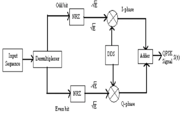
The digital QPSK modulator is as shown in Fig 1. The input binary data sequence is divided into two other sequences i.e., odd and even numbered bits of the input sequence. These two sequences are in unipolar then changed into bipolar by using Non Return to Zero (NRZ) encoding technique. The coded data will be mixed with carrier which is generated from Direct Digital Synthesizer [DDS] as in Fig 1. The DDS produces the sine and cosine as separate carrier signal with same frequency. After multiplying the carrier with bipolar data, the obtained odd data will be known as I-phase and the even data as Q-phase. These two phases will be added together to produce a single QPSK signal which is similar to the result obtained from (2).
Fig. 1: Digital QPSK Modulator block diagram.
3.
Proposed Methodology
Two new methods are proposed in QPSK modulators, first method uses BOOTH multiplication instead of arithmetic multiplication, up and down-accumulator for generating carrier wave instead of DDS. Second method uses ROM as main data storage to produce same QPSK signal as conventional modulator.
Proposed QPSK Modulator Method 1
219 odd and even data is multiplied with the carrier waves of sine and cosine, generated from the local oscillator. The design and implementation of the signed BOOTH multiplier is discussed in the following section.
BOOTH Multiplier Design
The input signal is multiplied with the carrier sine and cosine wave generated using the local oscillator. A signed multiplier is designed using BOOTH multiplier algorithm [9].
The BOOTH algorithm used to implement the signed multiplier is as follows:
Step 1:The multiplicand X and multiplier Y is loaded into a register. Bit adjustment is made with X and Y
so that bits length of X and Y are equal. Bit „0‟ is
padded in order to achieve it.
Step 2:An accumulator is used to store the result. The length of the accumulator should be twice the length of multiplicand or multiplier. A = 2X or 2Y.
Step 3:The multiplicand X is loaded into the accumulator from LSB.
Step 4:A dummy bit of 0 is appended with the accumulator A at the LSB
Step 5:During the multiplication operation, the pair of LSB of the accumulator and the dummy bit is considered to follow further arithmetic operations Step 6:Depending on the bit pair obtained in the previous step, following operations is performed:
“00” –Arithmetic shift right of the Accumulator.
“01”– Add multiplier Y to the Accumulator A (from MSB of A) and Arithmetic shift right of Accumulator.
“10”– Subtract multiplier Y from the Accumulator A (from MSB of A) and Arithmetic shift right of Accumulator.
“11”–Arithmetic shift right of the Accumulator. Shift operations are performed along with dummy bit. The above operations are continued till MSB of multiplicand X is shifted off from the accumulator A. In this section, 8-bit x 2-bit signed BOOTH multiplier is designed and implemented. These two phases will be added together to produce a single QPSK signal same as(2).
Proposed QPSK Modulator Method 2
For the second QPSK modulator architecture, the above proposed QPSK modulator 1 architecture will be constructed just to collect four different combinational input data for different phases of QPSK. Once the data is collected, the first proposed QPSK modulator architecture will not be used for future method. In this method, data for each QPSK is
collected and stored in four different ROM blocks. Each ROM will store data for one QPSK phase. Since all the four possible phases for a QPSK is stored in
four different ROM‟s, the digital QPSK modulator is no longer required to produce a QPSK phase from I and Q phase as in first method QPSK modulator. For the simulation purposes, a serial input sequence will be considered as input to the 1:2 demultiplexer. The 1:2demultiplexer will separate the input sequence into odd and even bits. These odd and even bits will be the input for the 4:1 multiplexer which will select one ROM for different combination of odd and even bits as shown in Fig.2.
Fig.2: Block diagram for proposed QPSK modulator
4.
Simulation
Proposed design and two method of conventional QPSK modulator is modeled with Verilog HDL and simulated on Xilinx ISE 9.1i platform. The crucial aspect for simulating the conventional QPSK modulator is to compare with the proposed QPSK modulator in term of high throughput i.e., timing, area and power utilization in FPGA. Each of the design Verilog HDL code is synthesized and tested with a ModelSimXE II 5.7g. The synthesizable code is translated into RTL (Register Transfer level) schematic diagrams while the Xilinx ModelSim simulator is used to run the top level code to obtain timing diagram. The simulator is used to produce the
binary or decimal data and also analog signal to plot the waveforms.
Conventional QPSK modulator
220 used and design 16 phases to generate sine and cosine wave.
Fig.3: Top level RTL for conventional QPSK modulator
Fig.4: Simulation result of conventional QPSK modulator
Proposed QPSK modulator 1
Fig.5 Shows the RTL schematic diagram and Fig.6 shows the timing diagram for proposed QPSK modulator method 1. In this method, the BOOTH multiplication is used and one phase needs 0.02µsec.Generating one cycle of sine wave requires 1µsec and this generates 50 samples by using up and down accumulator. The proposed QPSK modulator 1 does not require the Look up Table (LUT).
Fig.5: Top level RTL for proposed QPSK modulator 1
Fig.6: Simulation result of proposed QPSK Modulator 1
Proposed QPSK modulator 2
Fig.7 shows the RTL schematic diagram and Fig.8 shows the simulator timing diagram. Since the data for each QPSK phase is collected and stored in four different Read Only Memory (ROM) blocks. Once the four phases QPSK modulator data is collected from proposed QPSK modulator 1, conventional QPSK modulator is no longer required. A group of 2 bits is used to represent a phase in QPSK waveform. A total number of 50 data is stored in each ROM to represent a phase in QPSK wave. Fig.8 shows the baseband data transition form 00, 01, 11 and 10.
Fig.7: Top level RTL for proposed QPSK modulator2
Fig.8: Simulation result of proposed QPSK modulator2
5.
Results
221 used by the entire implementation is described inTable 2, Table 3, Table 4 and Table 5. The performance and area constraints have been improved in proposed method 2 compared to conventional QPSK modulator which is shown in Table 3 and Table 4.
Table 2: Conventional QPSK Modulator
Parameters Total Usag e Total available on FPGA % Usage
No. of slices 30 3,584 1%
No. of 4 input LUTs 46 7,168 1%
No. of slice Flip Flops 28 7,168 1%
Table 3: Proposed QPSK Modulator 1
Parameters Total Usage Total available on FPGA % Usage
No. of slices 50 3,584 1%
No. of 4 input LUTs 90 7,168 1%
No. o slice Flip Flops 39 7,168 1%
Table4:Proposed QPSK Modulator 2
Parameters Total Usage Total available on FPGA % Usage
No. of slices 120 3,584 3%
No. of 4 input LUTs 174 7,168 2%
No. o slice FlipFlops 55 7,168 1%
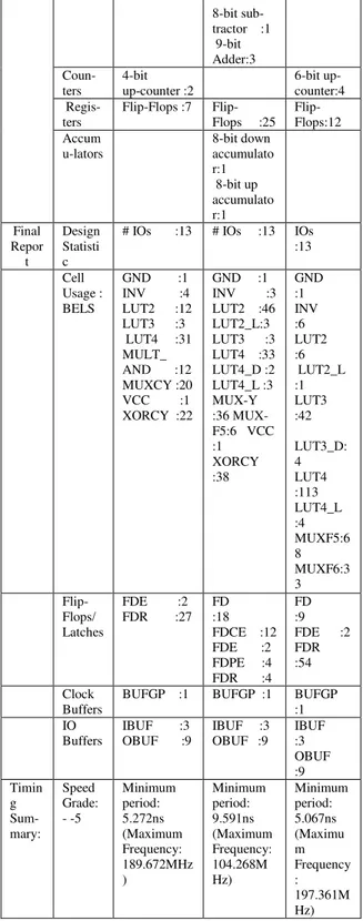
Table 5: Comparison of three methods of QPSK modulator Para- meters Convention al QPSK Modulator Proposed QPSK Modulator 1 Proposed QPSK Modulato r 2 Adva n-ced HDL Syn-thesis Repor t
ROMs 16x8-bit ROM :2 4x4-bit ROM :1
4x4-bit ROM :1
50x9-bit ROM :4
Multi 8x2-bit Registered multiplier :2
Mux 9-bit
4-to-1 mux :1 Adders / Subtrac -tors 9-bit adder :1 2-bit adder :30 8-bit adder :1 8-bit sub-tractor :1 9-bit Adder:3 Coun-ters 4-bit up-counter :2 6-bit up- counter:4 Regis-ters
Flip-Flops :7 Flip- Flops :25
Flip- Flops:12 Accum u-lators 8-bit down accumulato r:1 8-bit up accumulato r:1 Final Repor t Design Statisti c
# IOs :13 # IOs :13 IOs :13
Cell Usage : BELS
GND :1 INV :4 LUT2 :12 LUT3 :3 LUT4 :31 MULT_ AND :12 MUXCY :20 VCC :1 XORCY :22
GND :1 INV :3 LUT2 :46 LUT2_L:3 LUT3 :3 LUT4 :33 LUT4_D :2 LUT4_L :3 MUX-Y :36 MUX-F5:6 VCC :1 XORCY :38 GND :1 INV :6 LUT2 :6 LUT2_L :1 LUT3 :42 LUT3_D: 4 LUT4 :113 LUT4_L :4 MUXF5:6 8 MUXF6:3 3 Flip-Flops/ Latches
FDE :2 FDR :27
FD :18 FDCE :12 FDE :2 FDPE :4 FDR :4
FD :9 FDE :2 FDR :54
Clock Buffers
BUFGP :1 BUFGP :1 BUFGP :1 IO
Buffers
IBUF :3 OBUF :9
IBUF :3 OBUF :9
222
6.
Conclusion
Table 5 shows that the conventional QPSK modulator design utilizes multiplier, adder, subtractor, counter and filp-flops and also DDS is used. In this, area, timing and power is less utilized but output phases are not good compared to proposed method. In proposed QPSK modulator 1 multiplier, counter and LUT are not used for carrier generator, it is designed by using up and down accumulator. Instead of multiplier, BOOTH algorithm is used. In this only adder and shifter is used for multiplication but QPSK modulator output signal is better compared to first method. The proposed method will take four phases of data from the method 1. The collected 50 data from each phasesare stored in ROM and in this method it eliminates the DDS and multiplier. The proposed QPSK modulator 2 does not use multiplier, adder, subtractor and DDS, hence high throughput is achieved. Successfully simulated on Xilinx ISE 9.1i software and implemented in FPGA Spartan-3E board. The power consumption, timing and area utilization achieved in the proposed QPSK modulator 2 also gives a high throughput as shown in Table 5.
References
[1] Simon Haykin “Communication Systems”,
Fourth Edition, PSN, 2008.
[2] Samir Palnitkar, “Verilog HDL: A Guide to Digital Design and Synthesis”, 2ndEdition, Prentice Hall, 2003.
[3] Michael D.Ciletti “Advanced Digital Design with the Verilog HDL”,PHI, 2003.
[4] U.Meyer-Baese “Digital Signal Processing with Field Programmable Gate Arrays”, Third Edition, Springer, 2009.
[5] B.Krongold, TimomPfau, N.Kaneda and
S.C.Jeffrey Lee “Comparison between PS-QPSK
and PDM-QPSK with Equal Rate and
Bandwidth”, IEEE Photonics Technology Letters, Vol.24, No.3, pp.203-205 Feb, 2012.
[6] G.Elamary, G.Chester, J.Neasham, “A Simple Digital VHDL QPSK Modulator Designed Using
CPLD/FPGA for Biomedical Devices
Applications”, Proceedings of the World
Congress on Engineering 2009, Vol.1, ISBN:978-988, July, 2009, London, U.K.
[7] M.Kovac, J.Kolouch “BPSK, QPSK Modulator Simulation Model”, Thesis, Doctoral Degree Programme, FEEC BUT, 2004.
[8] A.M.Moubark,Mohd. Alauddin Mohd Ali,
HilmiSanusi and Sawal Md. Ali.“ FPGA
Implementation of Low Power Digital QPSK Modulator Using Verilog HDL”, Journal of
Applied Sciences (JAS-2013) Vol.13, Issue 3, pp.385-392, 2013.
[9] Chandrasetty, Vikram Arkalgud. VLSI Design: A
Practical Guide for FPGA and ASIC
Implementations. Springer, 2011.
[10]DOI:10.1007/978-1-4614-1120-8_2, Science + Business Media, ©Springer, LLC 2011.
[11] T.Sakla, D.Jain, S.Gautam “Implementation of
Digital QPSK Modulator By Using
VHDL/Matlab”, International Journal of Engineering Science and Technology, Vol 2, Issue 9, pp.4827-4831, 2010.
[12] A.M.Bhavikatti, SubhashKulkarni, UdayKalyani
“FPGA Implementation of -QPSK Modulator
and Demodulator”, International Journal of Computational Engineering & Management, Vol 15, Issue 4, July 2012.
K.Anitha received the Bachelor Degree in Electronics and Communication
Engineering from Institute of
Engineer,AMIE in 2011and currently pursuing M.Tech degree in Digital
Communication Engineering,
M.S.Ramaiah Institute of Technology, Bangalore, Karnataka, India.
Umesharaddy received the Bachelor
Degree in Electronics and
Communication Engineering from
Visvesvaraya Technological University, Belgaum, Karnataka, India, in 2003 and M.Tech degree in VLSI Design and Embedded Systems from Visvesvaraya Technological University, Belgaum, Karnataka, India, in 2006. He is currently working as Assistant Professor in the Department of Telecommunication Engeneering, M.S.Ramaiah Institute of Technology, Bangalore, Karnataka, India. His area of interest is VLSI Design with Communication.
Dr. B.K.Sujatha received the Bachelor
Degree in Electronics and
Communication Engineering from
Mysore University, Karantaka, India, in 1987, M.E. Degree in Electronics Engineering from Bangalore University, Bangalore in 1993 and Ph.D Degree in Electronics and
Communication Engineering from Visvesvaraya
Technological University, Belgaum, Karnataka, India, in 2006. She is currently working as Professor in the
Department of Telecommunication Engineering,
M.S.Ramaiah Institute of Technology, Bangalore,