UNIVERSIDADE NOVA DE LISBOA
Faculdade de Ciˆ
encias e Tecnologia
Departamento de Engenharia Electrot´
ecnica e de
Computadores
Design of a Continuous-Time (CT)
Sigma-Delta (
Σ∆
) Modulator for
Class D Audio Power Amplifiers
Por
Jo˜
ao Lu´ıs Alvernaz de Melo
Disserta¸c˜ao apresentada na Faculdade de Ciˆencias e Tecnologia
da Universidade Nova de Lisboa para obten¸c˜ao do Grau
de Mestre em Engenharia Electrot´ecnica e de Computadores.
Orientador: Doutor Nuno Filipe Silva Ver´ıssimo Paulino
3
`
Agradecimentos
Ao terminar esta tese resta-me registar os momentos mais marcantes e agradecer
a todas as individualidades que de v´arias formas contribu´ıram para a conclus˜ao da
mesma. Os momentos mais marcantes, em termos de decis˜oes, foram quando deixei
na ilha do Pico fam´ılia e amigos para vir para Lisboa h´a 11 anos e, h´a 6 anos, ter
interrompido o meu antigo e motivante trabalho para ingressar na faculdade.
Tenho como referˆencia e motiva¸c˜ao o trabalho ´arduo e incas´avel dos meus pais, o
que foi muito importante em todas as fases da minha vida. N˜ao posso deixar de
agradecer aos meus irm˜aos e irm˜as, Isilberta, Jorge, Paulo e L´ıdia, ao meu tio Lu´ıs,
bem como, enviar um carinho muito especial aos meus av´os Am´elia e Manuel que
infelizmente partiram durante a fase do curso.
Existe uma quantidade de amigos espalhados por todo o Mundo que gostaria de
mencionar, no entanto e felizmente, n˜ao existe espa¸co suficiente para o fazˆe-lo. As
noitadas, as festas, as viagens, os bons e maus momentos foram sempre em grande
parte compartilhados com eles, em especial, a ”malta da Terra do P˜ao”.
A n´ıvel acad´emico, um obrigado aos v´arios colegas com quem tive o privil´egio de
trabalhar e estudar bem como ao NEEC. Agrade¸co ao Professor Nuno Paulino
(ori-entador) pela sua dedica¸c˜ao e empenho no apoio prestado durante a realiza¸c˜ao desta
tese.
A todos o meu profundo muito obrigado.
Sum´
ario
A crescente procura por equipamentos port´ateis com recursos de ´audio ´e uma
reali-dade. Estes equipamentos precisam de amplificadores de potˆencia de ´audio para
pro-duzir som atrav´es de pequenos alto-falantes ou auscultadores. Como estes
equipa-mentos dependem de baterias para a sua pr´opria alimenta¸c˜ao, o uso de
amplifi-cadores de ´audio extremamente eficientes ´e de relevante importˆancia, tal como
re-duzir o calor gerado pelo amplificador de potˆencia, de modo que dissipadores de
calor volumosos possam ser eliminados, permitindo uma redu¸c˜ao de tamanho aos
equipamentos.
Amplificadores lineares, como os de Classe AB, embora exibam uma alta
lineari-dade, possuem baixo rendimento, especialmente para n´ıveis reduzidos de potˆencia.
Amplificadores de Classe D podem atingir um alto rendimento, j´a que os trans´ıstores
de sa´ıda s˜ao utilizados como interruptores e, portanto, a dissipa¸c˜ao de potˆencia ´e
idealmente zero. Um dos principais desafios no projecto de amplificadores de Classe
D ´e a concep¸c˜ao do modulador, que codifica o sinal anal´ogico de entrada em uma
sequˆencia de pulsos usados para produzir o sinal de potˆencia da sa´ıda. O espectro da
sequˆencia de pulsos cont´em o sinal de ´audio pretendido, bem como, as componentes
indesej´aveis (mas inevit´aveis) de alta frequˆencia.
Este trabalho apresenta um modulador Sigma-Delta de terceira ordem com 1,5-bit
com realimenta¸c˜ao distribu´ıda e desloca¸c˜ao de zeros para amplificadores de ´audio
de Classe D. A fim de melhorar a rela¸c˜ao sinal-ru´ıdo (SNDR), sem aumentar
signi-ficativamente a sobre amostragem (OSR) ou a ordem do modulador (n˜ao superior a
8
3), o modulador usa desloca¸c˜ao de zeros e 1,5-bit de quantiza¸c˜ao.
Abstract
An increasing demand for portable media devices with audio capabilities is the
reality today. These devices need audio power amplifiers to produce sound trough
speakers or earphones. Since these devices rely on batteries for their energy needs,
the use of extremely efficient audio amplifiers is of paramount importance. It is also
important to reduce the heat generated by the power amplifier itself, so that the
bulky heat sink can be eliminated, thus allowing for small size portable devices.
Linear amplifiers, such as class AB, have high linearity, but have low efficiency
espe-cially for lower power levels. Class D amplifiers can achieve high efficiencies because
the power devices are used as switches and therefore their power dissipation is,
ide-ally, zero. One of the main challenges in the design of class D amplifiers is designing
the modulator circuit that encodes the input analogue signal into a switching
se-quence used to produce the output power signal. The spectrum of the switching
sequence contains the desired audio signal plus undesired (but unavoidable)
high-frequency content.
This work presents a 3rd order 1.5-bit Σ∆ modulator with distributed feedback
and local resonator feedback for Class D audio amplifiers. In order to improve
the signal-to-noise-and-distortion ratio (SNDR), without increasing significantly the
oversampling ratio (OSR) or the order of the modulator (not greater then 3), the
modulator uses transmission zeros and 1.5-bit quantization.
Keywords:
Continuous-Time (CT) Sigma-Delta (Σ∆), Class D
am-plifier, Audio.
Contents
Agradecimentos 5
Sum´ario 7
Abstract 9
List Of Acronyms 15
List of Figures 19
List of Tables 21
1 Introduction 23
1.1 Motivation . . . 23
1.2 Audio Amplifiers . . . 24
1.2.1 Introduction . . . 24
1.2.2 Class A . . . 25
1.2.3 Class B . . . 25
1.2.4 Class AB . . . 26
1.2.5 Class D . . . 27
1.3 Thesis Objectives and Contributions . . . 27
1.4 Thesis Structure . . . 27
2 Class D Amplifiers 29 2.1 Introduction . . . 29
2.1.1 Important Factors in Audio Class D Design . . . 30
2.2 Sound Quality . . . 30
2.3 Modulation Technique . . . 31
2.3.1 Pulse Width Modulation (PWM) . . . 31
2.3.2 Pulse Density Modulation (PDM) . . . 32
2.3.3 Self-Oscillating Modulation . . . 33
12 CONTENTS
2.4 Output Power Stage . . . 34
2.5 EMI Considerations . . . 35
2.6 LC Filter . . . 36
2.6.1 Design . . . 37
2.7 Total system cost . . . 39
2.8 System Specifications . . . 40
3 Sigma-Delta Modulation 41 3.1 Introduction . . . 41
3.2 Σ∆ ADC Basic Concepts . . . 42
3.2.1 Sampling and Quantization . . . 42
3.2.2 First order CT-Σ∆ Modulator . . . 44
3.3 Study of 3rd Order CT-Σ∆ Modulators . . . 46
3.3.1 1-bit with Distributed Feedback . . . 47
3.3.2 1-bit with Distributed Feedback and Local Resonator Feed-back . . . 48
3.3.3 1.5-bit with Distributed Feedback . . . 50
4 Proposed Architecture 53 4.1 Introduction . . . 53
4.2 Theoretical Analysis . . . 54
4.3 Circuit Design . . . 57
4.3.1 ADC Design . . . 60
4.3.2 Important Parameters in Operational Amplifiers . . . 62
4.4 Monte Carlo Analysis of the Circuit . . . 65
4.5 Simulation Results . . . 66
5 Conclusions and Future Work 69 5.1 Conclusions . . . 69
5.2 Future Work . . . 70
CONTENTS 13
D.2 JMCS, 2010 . . . 91
List Of Acronyms
A/D, ADC Analog-to-Digital Converter
CT Continuous Time
DR Dynamic Range
DT Discrete Time
GBW Gain-Bandwidth Product
NTF Noise Transfer Function
OSR Over-Sampling Ratio
PCB Printed Circuit Board
PSNR Peak SNR
PSRR Power Supply Rejection Ratio
PWM Pulse-Width Modulation
SDM Sigma-Delta Modulation
SNDR Signal-to-Noise and Distortion Ration
SNR Signal-to-Noise Ratio
STF Signal Transfer Function
THD Total Harmonic Distortion
List of Figures
1.1 Class A Amplifier. . . 25
1.2 Class B Amplifier. . . 26
1.3 Class AB Amplifier. . . 26
2.1 Class D open-loop-amplifier block diagram. . . 29
2.2 Analog PWM generator. . . 32
2.3 Principle scheme of an basic Self-Oscillating amplifier. . . 33
2.4 Half-bridge output stage with LC low-pass filter. . . 34
2.5 Full-bridge output stage with LC low-pass filter. . . 34
2.6 Filter arrangements for the full-bridge output stage. (a) is the sim-plest but allows a common-mode signal on the speaker cabling. (b) and (c) are the most usual versions. (d) is a four-pole filter. . . 36
2.7 LC low-pass filter for single-ended. . . 37
2.8 Combination of two half-bridge in to a full-bridge topology. . . 38
3.1 Quantization error (en) when the quantization interval is defined by the midpoint. . . 43
3.2 Block Diagram of the 1st order Σ∆ modulator . . . 44
3.3 NTF and STF of the 1st order Σ∆ modulator . . . 45
3.4 Block diagram of the 3rd order 1-bit Σ∆ modulator with distributed feedback. . . 47
3.5 Output spectrum of the 3rd order 1-bit Σ∆ modulator with dis-tributed feedback (219 points FFT using a Blackman-Harris window). 48 3.6 Block diagram of the 3rd order 1-bit Σ∆ modulator with distributed feedback and local resonator feedback. . . 49
3.7 Output spectrum of the 3rd order 1-bit Σ∆ modulator with dis-tributed feedback and local resonator feedback (219 points FFT using a Blackman-Harris window). . . 49
18 LIST OF FIGURES
3.8 Block diagram of the 3rdorder 1.5-bit Σ∆ modulator with distributed
feedback. . . 50
3.9 Output spectrum of the 3rd order 1.5-bit Σ∆ modulator with dis-tributed feedback (219 points FFT using a Blackman-Harris window). 51 4.1 Block diagram of the 3rd order 1.5-bit Σ∆ modulator (mathematical model) with distributed feedback and local resonator feedback. . . 54
4.2 Output spectrum of the 3rd order 1.5-bit Σ∆ modulator with dis-tributed feedback and local resonator feedback (219points FFT using a Blackman-Harris window). . . 56
4.3 Conversion of the mathematical model into the electrical model. . . . 57
4.4 Schematic design of the modulator. . . 58
4.5 Bode diagram of the STF of the modulator. . . 59
4.6 Bode diagram of the NTF of the modulator. . . 59
4.7 Schematic design of 1.5-bit quantizer. . . 60
4.8 Measured SNDR as function of threshold voltage (Vt). Data obtained by running 1000 simulations with a Vt step of 0.4 mV. . . 61
4.9 Histogram of the behavioral simulated SNDR of the proposed Σ∆ modulator (3σvt = 10 mV) . Data obtained by running 500 Monte-Carlo simulations of the proposed architecture. . . 61
4.10 Encoding logic for 1.5-bit quantizer. . . 62
4.11 Influence of the DC gain in the output spectrum of the modulator (results obtained with electrical simulations with first order model amplifier with a GBW = 50 MHz, and a slew rate = 10 V/µs). . . 63
4.12 Influence of the GBW in the output spectrum of the modulator (re-sults obtained with electrical simulations with first order model am-plifier with a DC gain = 72 dB, and a slew rate = 10 V/µs). . . 64
4.13 Influence of the slew rate in the output spectrum of the modulator (results obtained with electrical simulations with first order model amplifier with a DC gain = 72 dB, and a GBW = 50 MHz). . . 64
4.14 Histogram of the behavioral simulated SNDR of the proposed Σ∆ modulator with component values mismatch. Data obtained by run-ning 500 Monte-Carlo simulations of the proposed architecture. . . . 65
4.15 Histogram of the behavioral simulated output voltage of the (a) first integrator, (b) second integrator, and (c) third integrator for the pro-posed Σ∆ modulator. . . 66
LIST OF FIGURES 19
4.17 Output spectrum of the proposed architecture obtained with electrical simulations with first order model amplifier with a DC gain = 72 dB, a GBW = 50 MHz, and a slew rate = 10 V/µs (216 points FFT using
a Blackman-Harris window). . . 67
4.18 Measured SNDR as function of Input Level. . . 68
A.1 Simulink circuit of the proposed architecture. . . 71
C.1 Proposed architecture. . . 79
C.2 Filter of the proposed architecture. . . 79
List of Tables
4.1 Coefficients of the proposed architecture. . . 56
4.2 Selected passive component values. . . 58
4.3 ADC codification. . . 60
4.4 Logic codification of the 1.5-bit quantizer. . . 62
5.1 Comparison of similar architectures. . . 70
Chapter 1
Introduction
1.1
Motivation
Due to the major concerns of global sustainability, there is a growing need for energy
saving. The energy efficiency of audio amplifiers can be an important contribution
to this end. Furthermore, the increasing demand for portable media devices with
audio capabilities is a reality. These devices need audio power amplifiers to produce
sound trough small speakers or earphones. Since these devices rely on batteries for
their energy needs, the use of extremely efficient audio amplifiers is of paramount
importance. It is also important to reduce the heat generated by the power amplifier
itself, so that the bulky heat sink can be eliminated, thus allowing for small size
portable devices.
Linear amplifiers, such as class AB, have high linearity, but have low efficiency
espe-cially for lower power levels. Class D amplifiers can achieve high efficiencies because
the power devices are used as switches and therefore their power dissipation is,
ide-ally, zero [1] [2]. The efficiency advantage of the Class D amplifiers is unquestionable
and, through this trait, this Class of amplifier has earned much interest.
24 CHAPTER 1. INTRODUCTION
1.2
Audio Amplifiers
1.2.1
Introduction
The most important characteristics of an amplifier are efficiency, linearity, output
power, and signal gain. Typically, there is a trade-off between these characteristics.
Understanding these trade-offs is an essential step in the designing process of an
audio amplifier.
Power Efficiency
The power efficiency is defined as
η= Pload
Psource ·100% (1.1)
where Pload is the average power delivered to the load and Psource is the average
power supplied by the source. The average power is given by
Pavg = T1
Z T
0
p(t)dt
and where T is the period of the signal.
Linearity
An amplifier is linear if it preserves the details of the signal waveform, such that,
Vout(t) =G·Vin(t)
where,VoutandVinare the output and input signals respectively, and G is a constant
1.2. AUDIO AMPLIFIERS 25
1.2.2
Class A
Class A amplifiers have the best linearity characteristic of all ( for a theoretical point
of view) but also has the lowest efficiency that ideally can not be larger than 50%.
This is due to the fact that the output transistors are always ON (see Figure 1.1). To
achieve high linearity and gain, the amplifier base and drain DC voltage should by
chosen correctly so that the amplifier operates in the linear region, meaning that the
bias current should be equal to the maximum load current. The device, since it is
turn on (conducting), is constantly carrying current, which represents a continuous
loss of power in the amplifier and consequently, a degradation of efficiency.
+VCC
-VCC
Figure 1.1: Class A Amplifier.
1.2.3
Class B
Class B (depicted in Figure 1.2) is characterized by biasing the output transistors
on the edge of the cut-off region resulting in a bias current of zero. This increases
the efficiency of the circuit, ideally, to 78.5%. The transistors only drive current
when they are excited by the input signal.
Essentially, this Class of amplifier implements two devices in the output stage in a
”push-pull” configuration, with each amplifying half of the waveform and operating
in strict time alternation. This configuration provides much greater efficiency than
26 CHAPTER 1. INTRODUCTION
wave-form can create distortion because one device must change from the ON region
to the cut-off region while the other device changes form the cut-off region to the
ON region. Any asymmetry in this transition leads to part of the signal to be cut.
+VCC
-VCC
ON
VB
ON
VB
Figure 1.2: Class B Amplifier.
1.2.4
Class AB
The Class AB is an intermediate class between class A and B where, the output stage
devices are biased with a DC current larger then 0, thus minimizing the crossover
distortion. In this case, there is a current in the output transistors (bias current)
which is smaller, when compared to the bias current of Class A, so that the efficiency
is close to Class B.
+VCC
-VCC
1.3. THESIS OBJECTIVES AND CONTRIBUTIONS 27
Figure 1.3 shows the Class AB amplifier with two bias voltages to avoid crossover
distortion. This Class is frequently used in audio amplifiers.
1.2.5
Class D
Class D amplifiers differ fundamentally from the more familiar classes of A, B, and
AB. In this Class of amplifier the output devices do not operate in the linear mode.
Instead the output transistors are operated as switches. When a transistor is off,
the current through it is zero. When it is on, the voltage across it is very small,
ideally zero. In each case, the power dissipated (P = V ×I) as the heat in the transistor is very low. This increases the efficiency, therefore requiring less power
from the power supply and smaller heat sinks for the amplifier. The main drawback
of this class of amplifier is the distortion and noise introduced into the signal by the
switching operation of the power stage. A broad overview of class D amplifiers will
be studied in Chapter 2.
1.3
Thesis Objectives and Contributions
The main objective of this thesis is to research and design of a Continuous-time
(CT) Sigma-Delta (Σ∆) modulator for Class D audio power amplifiers. This work
gives an important contribution of personal knowledge acquired and to the scientific
community as a result of the published papers.
1.4
Thesis Structure
After a brief introduction, the remainder of the dissertation is organized as follows.
Chapter 2 gives a general overview of the Class D amplifiers. Sigma-Delta
modula-tion and several architecture opmodula-tions for the modulator will be studied in Chapter
28 CHAPTER 1. INTRODUCTION
3 in order to improve the SNDR value, and also, explains the steps necessary to
design the circuit implementation of the proposed Σ∆ modulator, and shows the
electrical simulations results of the modulator circuits. Finally, Chapter 5 concludes
Chapter 2
Class D Amplifiers
2.1
Introduction
Typically, a Class D amplifier (Figure 2.1) consists of two stages. The first stage is
a signal processing stage that converts the input audio signal into a two-level (1-bit)
signal. This two-level signal represents a Pulse-Width Modulation (PWM) signal or
a Pulse-Density Modulation (PDM) signal. The second stage of the amplifier is a
power output stage, in which the two-level signal drives the output power MOSFETs
(half-bridge or full-bridge).
MODULATOR SWITCHING SPEAKER
OUTPUT STAGE
LOW-PASS FILTER
(LC) ( )
in
v t dout( )n yout( )n vout( )t
Figure 2.1: Class D open-loop-amplifier block diagram.
The Class D amplifier dissipates much less power than the traditional Class A/AB.
The output stage devices switches between the positive and negative power supplies
so as to produce a train of voltage pulses. This waveform reduces the power
dissi-pation of the amplifier, because the output transistors have zero current when not
switching, and have lowVDS when they are conducting current, thus resulting in a
30 CHAPTER 2. CLASS D AMPLIFIERS
smaller power dissipation (VDS×IDS) in the amplifier. Due to the binary switching
of the output devices of the amplifier, the output signal of the amplifier contains
high frequency components. These components must be filtered in order to reduce
the electromagnetic energy radiated by the amplifier, typically, a LC filter is used
for this function.
2.1.1
Important Factors in Audio Class D Design
The strongest motivation to use Class D for audio applications is the low power
dissipation, but there are important challenges in the design of this type of amplifiers.
These include:
• Sound quality
• Modulation techniques
• Electromagnetic interference (EMI)
• LC filter design
• Total system cost
• System specifications
2.2
Sound Quality
To achieve a good sound quality in Class D audio amplifiers, some issues must be
taken into account.
The sound quality of an audio amplifier is fundamentally determined by its
perfor-mance in term of distortion (e.g. THD) and noise (e.g. PSRR). One of the problems
with open-loop Class D amplifier is the propensity of the output stage to introduce
non-linearities and noise into the signal [3]. The non-linearity and noise will, as a
2.3. MODULATION TECHNIQUE 31
The Power-supply noise couples almost directly to the speaker with very small
re-jection. This occurs because the output stage transistors connect the power supplies
to the low-pass filter through a very low resistance. The filter rejects high-frequency
noise, but is designed to allow all audio frequencies, including the low frequencies
from the Power-supply (noise). However, there are good solutions to these problems.
Using singe-loop feedback with high loop gain (as is done in many linear amplifiers)
or double-loop feedback contributes a lot for a better performance [4]. Feedback
from the LC filter input will significantly improve PSRR and attenuate all
non-LC-filter distortion mechanisms. LC non-LC-filter nonlinearities can be attenuated by including
the speaker in the feedback loop. On the other hand, the use of a loop feedback
complicates the amplifier design.
2.3
Modulation Technique
The first step in designing a switching amplifier is the choice of the modulation
technique.
One of the main challenges in the design of class D amplifiers is designing the
mod-ulator circuit that encodes the input analogue signal into a switching sequence used
to produce the output power signal. The spectrum of the switching sequence
tains the desired audio signal plus undesired (but unavoidable) high-frequency
con-tent. The three most common architectures used to implement the modulator are:
pulse-width modulation (PWM) [3] with a triangle-wave (or saw-tooth) oscillator,
self-oscillating modulation [5] and Sigma-Delta Modulation [6] [7] (SDM).
2.3.1
Pulse Width Modulation (PWM)
Pulse-width modulation is the most common modulation technique, as shown in
Figure 2.2. Conceptually, PWM compares the input audio signal to a triangular or
32 CHAPTER 2. CLASS D AMPLIFIERS
the carrier frequency within each period of the carrier, the duty-cycle ratio of the
PWM pulse is proportional to the amplitude of the input signal . This sampling
process is called natural sampling. One challenge in this case is to generate a linear
carrier to minimize harmonic distortion, this can be particulary hard for large carrier
frequencies.
This modulation technique is attractive because the concept is simple and it allows
high SNR on audio-band; however, PWM has several problems: The PWM process
inherently adds distortion in many implementations [8], also, harmonics of the PWM
carrier frequency produce electromagnetic interference (EMI).
Comparator Low
High Input signal
Chopping (carrier) signal
Figure 2.2: Analog PWM generator.
2.3.2
Pulse Density Modulation (PDM)
A PDM signal can be generated using a (Σ∆) modulator. The modulator uses a
low resolution quantizer (typically 1-bit) to produce a digital signal from the input
signal. The filter in the modulator has a high-pass transfer function that removes
the quantization noise from the lower frequencies and transfers it to the higher
frequencies. The high frequency quantization noise can be eliminated by a low pass
filter. Sigma-Delta modulators are very well known and are the chosen architecture
for A/D converter of audio signals and therefore the design of these type of circuits
is very well understood [7]. A broad overview of Σ∆ Modulation will be presented
2.3. MODULATION TECHNIQUE 33
2.3.3
Self-Oscillating Modulation
Self-oscillating amplifiers use the feedback loop to create their own clock signal,
in-stead of using an externally provided clock [5]. The properties of the loop determine
the variable switching frequency of the modulator. An outstanding audio quality
is possible thanks to the feedback; nevertheless, the loop is self-oscillating, so it’s
difficult to synchronize with any other switching circuits, or to connect to digital
audio sources without first converting the digital to analog. Figure 2.3 depicts the
principle of an self-oscillating amplifier.
Loop Filter
L
C
Comparator Digital
Buffer ( )
in V t
e
Figure 2.3: Principle scheme of an basic Self-Oscillating amplifier.
The basic building block consists of a comparator, a loop filter and a digital buffer.
The comparator is not clocked, so the loop is fully analog. The loop filter is
con-structed so the loop is unstable. A limit cycle oscillation exists in the loop, resulting
in a square wave output with a determined frequency. When this unstable system
is forced by an external signal (Vin) with a frequency lower than this self-oscillation
frequency, the limit cycle acts as dither and linearizes the system as long as the error
signal (e) at the inputs of the comparator is smaller than the limit cycle amplitude
at the comparator input. The output is a square wave containing the limit cycle
frequency and the forced signal. The transfer function of the linearized system is
34 CHAPTER 2. CLASS D AMPLIFIERS
2.4
Output Power Stage
The output stage of the Class D amplifiers are usually implemented using two
topolo-gies: half-bridge or full-bridge configurations. Each topology has advantages and
disadvantages.
DC
Figure 2.4: Half-bridge output stage with LC low-pass filter.
In brief, a half-bridge (depicted in Figure 2.4) is potentially simpler and requires a
simpler low pass filter, however the current drawn from the power supplies is signal
dependent and therefore a signal replica can appear in the power supply voltages
which can cause distortion. In order to reduce this effect it is necessary to filter the
signal from the power supply using large capacitors.
DC M1
M4 M3
M2
Figure 2.5: Full-bridge output stage with LC low-pass filter.
The full-bridge is shown in Figure 2.5). This topology requires two half-bridge
2.5. EMI CONSIDERATIONS 35
current from the power supply and therefore does not introduce the signal in the
power supply, which improves the circuit performance and simplifies the design of
the power supply circuit. Another advantage of the full-bridge configuration is the
absence of the offset, which means that zero DC current flows at the output and
consequently improving the global power dissipation. Also, this configuration allows
1.5-bit quantization and the corresponding three-level quantization can be described
as:
1. [−1]→ green path (M2 to M3)
2. [ 0]→ red path (M3 to M4 or M4 to M3) 3. [+1]→blue path (M1 to M4)
2.5
EMI Considerations
The high-frequency components of the switching signal in a Class D amplifier
out-puts requires serious consideration. If not properly understood and managed, these
components can generate large amounts of electromagnetic interference (EMI) and
disrupt operation of other electrical equipment nearby.
The EMI can have two sources of origin: signals that are radiated into space and
those that are conducted via speaker and power-supply wires. A useful principle is
to minimize the area of loops that carry high-frequency currents, since the strength
of associated EMI is related to loop area and the proximity of loops to other circuits
[10]. The amount of power radiated from these loops is dependent of the loop area
when compared to the wavelength of the signals, therefore it is also important to
reduce the maximum frequency of the signals in the amplifier. This means that it
is very important to use a switching frequency as low as possible, corresponding to
36 CHAPTER 2. CLASS D AMPLIFIERS
2.6
LC Filter
The essential idea of the output filter of a Class D audio amplifier is to prevent the
radiation of the high frequency components of the switching output signal. Since
the energy of the unwanted signals is located at high frequencies this means using
a low-pass filter. The inductance of a loudspeaker coil alone will, in general, be
low enough to allow some of the switching-frequency energy to pass through it
to ground, causing significant losses [11]. A correctly designed output filter limits
supply current, protects the loudspeaker from switching waveforms and reduces EMI.
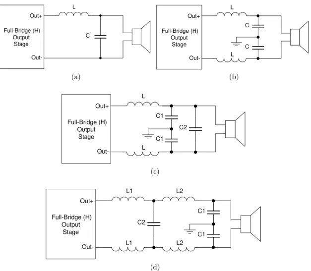
Full-Bridge (H) Output Stage Out+ Out-L C (a) Full-Bridge (H) Output Stage Out+ Out-L C C L (b) Full-Bridge (H) Output Stage Out+ Out-L C1 C1 L C2 (c) Full-Bridge (H) Output Stage Out+ Out-L1 C1 C1 L1 C2 L2 L2 (d)
2.6. LC FILTER 37
The use of an output full-bridge requires a somewhat more complex output filter. If
the simple two-pole filter of Figure 2.6a is used, the switching frequency is kept out
of the loudspeaker, but the wiring to it will carry a large common-mode signal from
the amplifier. A balanced filter is therefore commonly used, in either the Figure
2.6b or Figure 2.6c versions. Figure 2.6d illustrates a four-pole output filter.
2.6.1
Design
The design of the the low-pass filter for the Class D amplifier is based on a
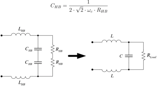
single-ended approach (Figure 2.7).
in
V
V
outHB
L
HB
C RHB
Figure 2.7: LC low-pass filter for single-ended.
The transfer function of the filter can be derived using a voltage divider equation in
which the load impedance is a parallel combination ofRHB and CHB.
H(s) = Vout(s) Vin(s)
=
RHB
s·RHB·CHB+1
RHB
s·RHB·CHB+1 +s·LHB
=
1
LHB·CHB
s2+s· 1
RHB·CHB +
1
LHB·CHB
(2.1)
A Butterworth approximation low pass filter for providing flat response in the pass
band can be chosen, which is critical for the audio system to improve its dynamic
performance. Equaling Equation 2.1 to the characteristic equation of a second-order
Butterworth filter in a standard form is obtained.
H(s) =
1
LHB·CHB
s2+s· 1
RHB·CHB +
1
LHB·CHB
= 1
38 CHAPTER 2. CLASS D AMPLIFIERS
Analyzing the Equation 2.2 an equation for CHB can be written as:
CHB =
1
2·√2·ωc ·RHB
(2.3)
HB L
HB
C RHB
HB R HB C HB L Load R C L L
Figure 2.8: Combination of two half-bridge in to a full-bridge topology.
Due to the combination of two half-bridge in to a full-bridge topology (depicted in
Figure 2.8) some relations can be done: C= CHB
2 and RLoad =RHB·2.
Replacing in Equation 2.3 theCHB forC·2 andRHB for RLoad2 the Equation for the
capacitor is given by:
C = 1
2·√2·ωc·RLoad
(2.4)
The value of the inductance remain the same, after the combination of two
half-bridge in to a full-half-bridge, and the expression for the LHB is given by:
LHB =
1 CHB
=
√
2·RHB
ωc →
L=LHB (2.5)
Typically, a 4 or 8 Ω resistor is assumed for the calculus of the filter components;
however, it is necessary to have in mind that, in reality, we have different speakers
with different types of frequency response. Due to this, is necessary to compensated
the filter variations with a proper network feedback design.
The output inductor should withstand the whole output current without saturation,
2.7. TOTAL SYSTEM COST 39
is an air-cone; nerveless, the size and number of turns required for the output stage
of Class D amplifiers makes it impractical, so a core has to be used in order to reduce
turn number and also provided a confined magnetic circuit. Powder cores or ferrite
cores can be used [12]. In Ferrite cores, it is necessary a ”gap” where the energy is
stored.
2.7
Total system cost
In the design of the Class D amplifiers it is necessary to have in mind the estimative
of the total system cost for the success of the product in terms of market share and
viability.
One way (and the most significant) to reduce the total system cost is the use of
the half-bridge topology for power stages in order to take advantage of the minor
complexity and reduced of material costs. Since a half-bridge is normally half of
a common full-bridge output, the quantity of power MOSFET’s and output filter
components is reduced by a factor of 2. However, the use of a half-bridge instead of
a full-bridge topology requires a DC-blocking capacitor at the output, hence highly
susceptible to noise on the power supply rail, and does not allow the use of 1.5-bit
quantization.
Another situation to have in mind is the choice of the tolerance of the resistors
(R) and capacitors (C) . The use of components mismatch with R=1% and C=5%
instead of R=5% and C=20%, increases the cost of those components (R and C)
in about 40%; however, the results will be better in terms of performance. This
analysis was based on prices from the online store RSr 1.
40 CHAPTER 2. CLASS D AMPLIFIERS
2.8
System Specifications
The sensitivity of the human ear is biased toward the lower end of the audible
frequency spectrum, around 3 kHz. Being 50 Hz, the bottom end of the spectrum,
and being 17 kHz, the top end at those limits, the sensitivity of the ear is reduced
by approximately 50 dB from the sensitivity at 3 kHz [13]. Taking advantage of
these features of the ear and considering that most people will not be able to hear
sounds above 16 kHz, the bandwidth of an audio amplifier, in reality, does not need
to be higher than 18 kHz.
A low switching frequency is important because it allows to use power transistors
with lower transition frequency (f T), thus lowering the cost. The behavior of the
transistor is similar to an ideal switch, when the switching frequency is lower. The
choice of fS have also to have in mind the limits of the frequency switching of the
IC drivers existing in the market2, in order to possibility the implementation of the
output stage with IC drivers and to not increase significantly the oversampling ratio
(OSR).
Chapter 3
Sigma-Delta Modulation
3.1
Introduction
Sigma-Delta (Σ∆) modulators are the most suitable A/D converters for low-frequency,
high-resolution applications, in view of their inherent linearity, reduced anti-aliasing
filtering requirements and robust analog implementation. Moreover, by trading
speed for accuracy, Σ∆ modulators allow high performance to be achieved with
low sensitivity to analog component imperfections and without need for component
trimming [14].
One of the advantages of Sigma-Delta Modulation (SDM) is that most of the
high-frequency energy in Sigma-Delta is distributed over a wide range of frequencies (not
concentrated in tones at multiples of a carrier frequency, as in PWM) providing
SDM with a potential EMI advantage over PWM.
Sigma-Delta Modulation can be implemented using Continuous-time (CT) or
discrete-time (DT) integrators. Compared to their discrete-discrete-time counterparts, CT-SDM’s
provide the added benefit of inherent anti-alias filtering and sampling error
suppres-sion [15]. Also, the gain-bandwidth product (GBW) and slew rate requirements of
the used amplifiers in CT are much lower compared to their DT. However, their
principal disadvantage is their sensitivity to clock jitter [16]. Several architectures
42 CHAPTER 3. SIGMA-DELTA MODULATION
options for a modulator in order to improve the signal-to-noise-and-distortion ratio
(SNDR) value, without increasing the oversampling ratio (OSR) or the order of the
modulator, can be implemented [17].
3.2
Σ∆
ADC Basic Concepts
This chapter is intended to give an basic introduction and overview of
analog-to-digital conversion (ADC), first in general and thereafter for the Σ∆ modulation, in
this case, the CT-Σ∆ modulator.
3.2.1
Sampling and Quantization
The process of the conversion of analog signals to the digital domain can be
sepa-rated in two operations [18]: the uniform sampling in time and the quantization in
amplitude. Assuming that the signal information of the continuous input signalx(t) is contained in the signal band (|fsig |≤fB wherefB is the signal bandwidth), the
sampling in time is a completely reversible process. The original signal (continuous
input signal) can be reconstructed without aliasing by simply low-pass filtering the
sampled signal, as long as the Nyquist Theorem is fulfilled (fS ≤2·fB =fN).
In the process of quantization in amplitude, a continuous range of analog values is
encoded into a set of discrete levels and the process of quantization is non-reversible.
The quantization process involved in A/D conversion is an inherently non-linear
operation and introduces errors to the conversion [19]; thus, the primary objective
in A/D converter design is to limit this error.
The Figure 3.1 shows the transfer function of an ADC or quantizer, and as previously
mentioned, is nonlinear. Considering that the input signal is random, that it changes
rapidly and that the number of quantization steps is large, then the quantization
error or noise (en) can be considered white noise. The quantization steps can be
defined as ∆ = F S
3.2. Σ∆ ADC BASIC CONCEPTS 43
Digital output
Analog input
n e
Figure 3.1: Quantization error (en) when the quantization interval is defined by the
midpoint.
bits. Thus, the quantization noise power can be expressed as:
e2rms =
1 ∆
Z −∆2 ∆
2
e2 de = ∆
2
12 (3.1)
The noise power spectral density (PSD) of the quantization is given by:
Se(f) =
e2rms fS
= ∆
2
12 · 1 fS
(3.2)
Oversampling
If an ideal low pass filter is used the SNR improves 3 dB each time the over-sampling
ratio is doubled (whereOSR = fS
2·fB ). A generic equation for the SNR is given by
[6]:
SN R= 6.02·B+ 1.76 + 10·log(OSR) (dB) (3.3) It is important to understand that this is an approximated expression due to the fact
that in reality the quantization noise is correlated to the input signal and therefore
44 CHAPTER 3. SIGMA-DELTA MODULATION
3.2.2
First order CT-
Σ∆
Modulator
The analysis of the sampling and noise theory, mentioned before, can now be used
to show how a Σ∆ modulator shapes quantization noise. The Block Diagram of the
1st order Σ∆ modulator principle is illustrated in Figure 3.2a.
( )
outd
n
( )
inv t
dt
( )
outy
t
ADC DAC(a) Σ∆ modulator principle.
1 s ( ) out Y s ( ) in V s ( ) q N s quantizer
(b) Linearized mathematical model.
Figure 3.2: Block Diagram of the 1st order Σ∆ modulator
The comparator of the circuit is represented in the sum node at the right of the
integrator and it’s here that sampling occurs and quantization noise is added.
Con-stantly, the output value is subtracted from its input signal and the result of this
operation is fed to the quantizer via an integrator. The feedback forces the average
value of the quantized output to track the average input. Any differences between
them accumulates in the integrator and the feedback loop will correct itself.
The main characteristic of a Σ∆ modulator is the different transfer behavior for the
quantization error signal, the noise transfer function (NTF) and the input signal
the signal transfer function (STF). Analyzing the mathematical model from Figure
3.2. Σ∆ ADC BASIC CONCEPTS 45
1. Letting Nq(s) = 0 for the moment, and solving for YVout(s)
in(s) is possible to obtain
the STF:
Yout(s) = [Vin(s)−Yout(s)]·
1 s
ST F = Yout(s) Vin(s)
=
1
s
1 + 1s = 1
s+ 1 (3.4)
2. By letting the signalVin(s) = 0 and solving for the YNoutq((ss)) the NTF is obtained:
Yout(s) =−Yout(s)·
1
s +Nq(s)
N T F = Yout(s) Nq(s)
= 1 1 + 1s =
s
s+ 1 (3.5)
Analyzing the Equations 3.4 and 3.5 above, they shows that indeed the oversampled
modulator acts as a low-pass filter for the input signal (showed in Figure 3.3a)
and a high-pass filter for noise. In Figure 3.3b is shown the noise shaping of the
oversampled 1st order Σ∆ modulator.
Frequency Ma g n it u d e (a) STF Frequency Ma g n it u d e (b) NTF
46 CHAPTER 3. SIGMA-DELTA MODULATION
3.3
Study of 3
rdOrder CT-
Σ∆
Modulators
The first step in the design of the modulator is choosing the order modulator, the
clock frequency value, and the bandwidth. Σ∆ modulators of orders higher than
2 are possible to design but they cannot simply be made by adding further stages
because the resulting system would, most likely, be unstable. In view of this problem,
the design procedure for finding the optimal 3rdΣ∆ modulator coefficients was based
on the described in [20]. Briefly, this methodology describes an empirical method
based on ordinary filter design that can be used to design high-order modulators.
Taking advantage of the features of the human ear described in Chapter 2 Section
2.8 and considering that most people will not be able to hear sounds above 16 kHz,
the bandwidth of an audio amplifier, in reality, does not need to be higher than 18
kHz. Therefore the modulator will be designed to have a signal bandwidth of 18 kHz
and a peak SNDR value with at least 80 dB (the SNDR is defined for a bandwidth
of 18 kHz).
As previously stated, it very important to use a low sampling frequency value in
order to reduce the EMI of the amplifier and also to avoid non-ideal effects in the
output devices during switching. A ideal 3rd Σ∆ modulator (assuming that it could
be stable) with an OSR value of 32 could theoretically produce an SNDR value of
around 95 dB. Therefore a sampling frequency value of 1.2 MHz is selected, resulting
in a OSR value of about 33.3.
However, due to the inherent instability of the modulator it is necessary to use a
transfer function that limits the noise shaping resulting in a lower SNDR value.
Therefore, several architecture options for the modulator will be studied in order to
3.3. STUDY OF 3RD
ORDER CT-Σ∆ MODULATORS 47
3.3.1
1-bit with Distributed Feedback
The block diagram of the 3rd order 1-bit Σ∆ modulator with distributed feedback,
implemented using CT integrators, is shown in Figure 3.4. The signal transfer
function (STF) of this structure is given by Equation 3.6 and will be essentially a
3rd order Butterworth low pass filter. The cut-off frequency of this filter function is
selected in order to limit the maximum gain of the NTF and eliminate the instability
of the modulator.
1 s 1 s 1 s ADC 1-bit DAC 1-bit ( ) out d n ( ) in v t 1
b b2 b3
( ) out
y t
Figure 3.4: Block diagram of the 3rd order 1-bit Σ∆ modulator with distributed
feedback.
The noise transfer function (NTF) given by Equation 3.7 was designed to be a 3rd
order Butterworth high-pass filter with a cut-off frequency of 99.6 kHz. The values
of the coefficients b1, b2 and b3 were calculated in order to implement the selected
Butterworth transfer function. The modulator was simulated usingSIM U LIN Kr
.
Each simulation calculated 219 points of the output signal and a fast Fourier
trans-formation using a Blackman-Harris window was applied in order ro complete the
output spectrum.
ST F = 1
s3+s2·b
3 +s·b2+b1
(3.6)
N T F = s
3
s3+s2·b
3+s·b2+b1
(3.7)
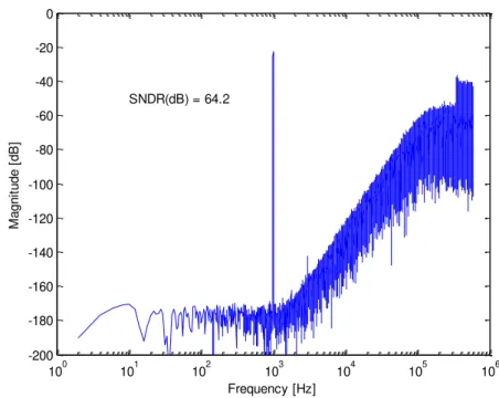
modu-48 CHAPTER 3. SIGMA-DELTA MODULATION
lator, obtained by simulation, in this case a maximum SNDR value of 64.2 dB was
obtained. The frequency of the sine wave input signal is 1 kHz.
100 101 102 103 104 105 106
-200 -180 -160 -140 -120 -100 -80 -60 -40 -20 0
SNDR(dB) = 64.2
Frequency [Hz] M a g n it u d e [ d B ]
Figure 3.5: Output spectrum of the 3rd order 1-bit Σ∆ modulator with distributed
feedback (219 points FFT using a Blackman-Harris window).
The low SNDR results from the low cut-off frequency of the filter which in term can
not be increased because the modulator would became instable.
3.3.2
1-bit with Distributed Feedback and Local Resonator
Feedback
One technique to improve the SNDR is to optimally distribute the zeros of NTF
inside the signal bandwidth, unlike the traditional design described above where
NTF zeros are all placed at DC. The architecture shown in Figure 3.6 allows
dis-tributing the zeros of NTF inside the signal bandwidth and can be designed using a
Chebyshev type II high-pass filter, in this case the stopband edge frequency of the
filter is 18 kHz. The coefficients b1, b2 and b3 determine the position of the poles
3.3. STUDY OF 3RD
ORDER CT-Σ∆ MODULATORS 49
not appear in the STF (Equation 3.8).
1 s 1 s 1 s ADC 1-bit DAC 1-bit ( ) out d n ( ) in v t 1
b b2 b3
( ) out
y t
Figure 3.6: Block diagram of the 3rd order 1-bit Σ∆ modulator with distributed
feedback and local resonator feedback.
ST F = 1
s3+s2·b
3+s·(α+b2) +b1
(3.8)
N T F = s·(s
2+α)
s3+s2·b
3+s·(α+b2) +b1
(3.9)
100 101 102 103 104 105 106
-200 -180 -160 -140 -120 -100 -80 -60 -40 -20 0
SNDR(dB) = 71.6
Frequency [Hz] M a g n it u d e [ d B ]
Figure 3.7: Output spectrum of the 3rd order 1-bit Σ∆ modulator with distributed
50 CHAPTER 3. SIGMA-DELTA MODULATION
The Figure 3.7 shows the output spectrum of the 3rd order 1-bit Σ∆ modulator with
distributed feedback and local resonator feedback, obtained by simulation, in this
case a maximum SNDR value of 71.6 dB was obtained. As expected, the shift of
the zeros from DC to the signal bandwidth improved the maximum SNDR value.
3.3.3
1.5-bit with Distributed Feedback
Another option to improve the SNDR is use a 1.5-bit quantizer (corresponding to
three-level quantization) instead of 1-bit quantizer. The increase of the resolution
of the quantizer improves the linearity of the feedback in the modulator. Since this
results in a more stable loop, it is possible to use a larger cut-off frequency in the
modulator and therefore improve the maximum SNDR value. In this case a cut-off
frequency of 133.2 kHz was selected. The use of three levels also reduces unnecessary
switching of the full-bridge output stage so that the switching loss is minimized.
1
s
1
s
1
s
ADC 1.5-bit
DAC 1.5-bit
( ) out
d n
( ) in
v t
1
b b2 b3
( ) out
y t
Figure 3.8: Block diagram of the 3rd order 1.5-bit Σ∆ modulator with distributed
feedback.
Figure 3.9 shows the simulated output spectrum of the 3rd order 1-bit Σ∆
modu-lator with a 1.5-bit quantizer, in this case a maximum SNDR value of 76.9 dB was
obtained. As expected the increase in the resolution of the quantizer improved the
3.3. STUDY OF 3RD
ORDER CT-Σ∆ MODULATORS 51
100 101 102 103 104 105 106
-200 -180 -160 -140 -120 -100 -80 -60 -40 -20 0
SNDR(dB) = 76.9
Frequency [Hz]
M
a
g
n
it
u
d
e
[
d
B
]
Figure 3.9: Output spectrum of the 3rdorder 1.5-bit Σ∆ modulator with distributed
Chapter 4
Proposed Architecture
4.1
Introduction
In order to obtain a maximum SNDR value with at least 80 dB, the topologies
described in Chapter 3 Section 3.3 (3rdorder 1-bit Σ∆ with distributed feedback and
local resonator feedback and the 3rdorder 1.5-bit Σ∆ with distributed feedback) were
combined into the same modulator (Figure 4.1). The loop filter in the modulator was
designed to have a stopband edge frequency of 18 kHz and a stop band attenuation
of 58.5 dB, with a sampling frequency (fS) of 1.2 MHz.
The choice offS was based in Chapter 2 Section 2.8 were the limits of the frequency
switching of the IC drivers existing in the market and also a low switching frequency
is important for a better performance in terms off efficiency. Furthermore, the
stopband edge frequency of 18 kHz is based in Chapter 2 Section 2.8, were the
features of the ear and considering that most people will not be able to hear above
16 kHz, the bandwidth of an audio amplifier, in reality, does not need to be higher
than 18 kHz.
54 CHAPTER 4. PROPOSED ARCHITECTURE
4.2
Theoretical Analysis
( ) q N s quantizer 1 S k s T
( )
inv
s
1b b2 b3
( )
outy
s
0 k 2 S k s T 3 S k s T 1( )
y s
3
( )
y s
2
( )
y s
ref V
Figure 4.1: Block diagram of the 3rd order 1.5-bit Σ∆ modulator (mathematical
model) with distributed feedback and local resonator feedback.
Analyzing the Block diagram of the Figure 4.1 same equations can be writen in
order to obtain the signal transfer function (STF) and the noise transfer function
(NTF) of the proposed architecture.
Letting Nq(s) = 0 for the moment the equations for the outputs are:
y1(s) = [vin(s)·k0−b1·Vref ·yout(s)]·
k1
s·TS
y2(s) = [y1(s)−y3(s)·α−b2·Vref ·yout(s)]·
k2
s·TS
y3(s) = [y2−b3·Vref ·yout(s)]·
k3
s·TS
yout(s) =y3(s)
Solving the the system of Equations for yout(s)
vin(s) and for simplification assuming k1 =
k2 =k3 =TS the STF is obtained as:
ST F = yout(s) vin(s)
= k0
s3+s2·b
3·Vref +s·b2·Vref +b1 ·Vref
(4.1)
4.2. THEORETICAL ANALYSIS 55
y1(s) = [0−b1·Vref ·yout(s)]·
k1
s·TS
y2(s) = [y1(s)−y3(s)·α−b2·Vref ·yout(s)]·
k2
s·TS
y3(s) = [y2−b3·Vref ·yout(s)]·
k3
s·TS
yout(s) = Nq(s) +y3(s)
Assuming for simplification k1 = k2 =k3 = TS and solving for the yNout(s)
q(s) the NTF
is obtained as:
N T F = yout(s) Nq(s)
= s(s
2+α)
s3+s2·b
3·Vref +s·b2·Vref +b1·Vref
(4.2)
The NTF of the filter (Equation 4.2) allows distributing the zeros of NTF inside the
signal bandwidth and can be designed using a Chebyshev type II filter. In order
to implement the filter transfer function it was used the tool SIM U LIN Kr for
several simulations . The M AT LABr code synthesizing a CT Chebyshev type II
filter is:
[A, B] =CHEBY2(order, R, W n,′high′,′s′)
whereorder = 3 defines the NTF order of the filter, with the stopband ripple R = 58.5 dB and stopband edge frequencyW n = 18·103·2π [rad/s] and the ”’high’,’s’”
designs a CT high-pass filter. The Equation 4.3 gives the transfer function of the
high-pass filter obtained with the previousM AT LABr code.
N T F = s(s
2+ 9.574
·109)
s3+s2·1.334·106+s·8.999·1011+ 3.034·1017 (4.3)
Comparing the NTF of Equation 4.2 with the NTF of Equation 4.3 it is
56 CHAPTER 4. PROPOSED ARCHITECTURE
SIM U LIN Kr. Note that is necessary to adjust the stopband ripple to obtain a
maximum SNDR value and also a stable loop filter.
The Table 4.1 gives the coefficients values of the simulated architecture.
Table 4.1: Coefficients of the proposed architecture.
Coefficients
k0 k1 =k2 =k3 b1 b2 b3 α
0.0621 1 0.1756 0.6249 1.1120 0.0066
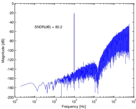
Figure 4.2 shows the output spectrum of the modulator, obtained by simulation, in
this case a maximum SNDR value of 80.2 dB was obtained. The combination of
all the previous techniques, studied in Chapter 3 Section 3.3, allowed to obtain a
maximum SNDR value with at least 80 dB using a 3rd order Σ∆ modulator with an
OSR value of approximately 32.
100 101 102 103 104 105 106
-200 -180 -160 -140 -120 -100 -80 -60 -40 -20 0
SNDR(dB) = 80.2
Frequency [Hz] M a g n it u d e [ d B ]
Figure 4.2: Output spectrum of the 3rd order 1.5-bit Σ∆ modulator with distributed
feedback and local resonator feedback (219 points FFT using a Blackman-Harris
4.3. CIRCUIT DESIGN 57
4.3
Circuit Design
It is necessary to design an electrical circuit that has the same behavior as the
architecture that was developed in the previous section.
Figure 4.3 shows a simple method to convert the mathematical model into the
electrical model. Note that theTS (F1S) is the period of the sampling frequency (FS
= 1.2 MHz).
1 S k s T ADC 1.5-bit DAC 1.5-bit ( ) out d n ( ) in v s 1
b b2 b3
( ) out y s 0 k 2 S k s T 3 S k s T 1 S k s T ( ) in v s 1 b 0 k 1 ( ) out y s ref V in R fb R C ref V
1( )
amp vo s ( ) in v s ) a )
b c)
1
Amp
Figure 4.3: Conversion of the mathematical model into the electrical model.
Analyzing the Figure 4.3.b) an equation for yout1(s) can be written as:
yout1(s) =
k0·k1
s·TS ·
vin(s)−
b1 ·k1
s·TS ·
vref(s) (4.4)
The equation for the output (voamp1(s)) of the integrator (depicted in Figure 4.3.c))
is given by:
voamp1(s) = −
1 s·Rin·C ·
vin(s)−
1 s·Rf b·C ·
vref(s) (4.5)
58 CHAPTER 4. PROPOSED ARCHITECTURE
an expression for Rin and Rf b. Note that the operational amplifier is considered
ideal in this approach.
Rin =
TS
k0·k1·C
, Rf b =
TS
b1·k1·C
(4.6)
The same idea can be applied to the other integrators blocks of the modulator
resulting in the modulator circuit shown in Figure 4.4. The values of the components
can be obtained using the approach previously described, assuming that all the
capacitors have a 1nF value.
Rin R11 R12 R 2 3 R2 1 R 2 2 C1 C2 C3 ( ) in v s
3( )
amp vo s R51 R53 R52 ( ) out y s 1 Amp 2 Amp 3 Amp 4 Amp ref
v vref
Figure 4.4: Schematic design of the modulator.
Table 4.2 gives all passive component values for the modulator.
Table 4.2: Selected passive component values.
Components
Id. Value Units C1 =C2 =C3 1 nF
Rin 13.3 kΩ
R11=R12 825 Ω
R23 4.75 kΩ
R22 1.33 kΩ
R21 750 Ω
R51=R52 10 kΩ
4.3. CIRCUIT DESIGN 59
In order to confirm the correct design of the modulator, the STF (Figure 4.5) and
NTF (Figure 4.6) of the modulator are obtained by performing two AC simulations
of the circuit of Figure 4.4, after replacing the quantizer by a wire.
100 101 102 103 104 105 106 107 108 -250 -200 -150 -100 -50 0 M a g n it u d e [ d B ] Frequency [Hz]
100 101 102 103 104 105 106 107 108 -300 -200 -100 0 100 200 P h a s e [ d e g re e s ] Frequency [Hz]
Figure 4.5: Bode diagram of the STF of the modulator.
100 101 102 103 104 105 106 107 108 -120 -100 -80 -60 -40 -20 0 20 Frequency [Hz] M a g n it u d e [ d B ]
100 101 102 103 104 105 106 107 108 0 50 100 150 200 250 Frequency [Hz] P h a s e [ d e g re e s ]
60 CHAPTER 4. PROPOSED ARCHITECTURE
4.3.1
ADC Design
The 1.5-bit quantizer (three levels) is realized by two comparators and is showed
in Figure 4.7. The output of the comparators is encoded to 1.5-bit representation
using the circuit shown in Figure 4.10. The threshold voltage for comparison is
determined by several simulations of the propose architecture in order to obtain the
max point of the SNDR as function of the threshold voltage. Figure 4.8 shows the
measured SNDR as function of threshold voltage (Vt), from this simulation results
the value of 0.36V was selected for Vt.
Vt Vt
Comp. 1
signal V
1
C
Out
2
C
Out
Comp. 2
Figure 4.7: Schematic design of 1.5-bit quantizer.
Table 4.3: ADC codification.
VSignal State OutC1 OutC2
VSignal > Vt +1 0 1
−Vt < VSignal < Vt 0 1 1
VSignal < Vt -1 1 0
Since the threshold voltage of the comparators has a random error, a Monte Carlo
analysis, where the Vt voltage of the comparators was randomly changed from the
selected nominal value with a 3σ value of 10 mV, was performed for 500 cases. The
histogram of the SNDR values obtained in this analysis is shown in Figure 4.9, this
histogram shows that the SNDR in the worst case only degrades about 0.8 dB with
4.3. CIRCUIT DESIGN 61
0.2 0.25 0.3 0.35 0.4 0.45 0.5 0.55 0.6
76 76.5 77 77.5 78 78.5 79 79.5 80 80.5
Threshold Voltage [V]
S N D R [ d B ]
Figure 4.8: Measured SNDR as function of threshold voltage (Vt). Data obtained
by running 1000 simulations with a Vt step of 0.4 mV.
79 79.2 79.4 79.6 79.8 80 80.2 80.4 80.6 80.8 81
0 20 40 60 80 100 120 N u m b e r o f O c c u rr e n c e s SNDR[dB]
Figure 4.9: Histogram of the behavioral simulated SNDR of the proposed Σ∆ mod-ulator (3σvt = 10 mV) . Data obtained by running 500 Monte-Carlo simulations of
62 CHAPTER 4. PROPOSED ARCHITECTURE
1 C
I
2 C
I
1
L
Dout
2
L
Dout
Figure 4.10: Encoding logic for 1.5-bit quantizer.
Table 4.4: Logic codification of the 1.5-bit quantizer.
IC1 IC1 State DoutL1 DoutL2
0 0 x 0 0
0 1 +1 0 1
1 0 -1 1 0
1 1 0 0 0
4.3.2
Important Parameters in Operational Amplifiers
In the previous analysis it was assumed that the operational amplifiers were ideal,
when real amplifiers are used the non-ideal effects can change the behavior of the
modulator. In order to understand what is the required performance of the different
parameters of the amplifiers, such as: gain-bandwidth product (GBW), slew rate and
DC gain, the modulator circuit was simulated using a first order electrical model for
the amplifiers. This model includes DC gain, a single pole and the slew rate effect.
In these simulations the amplifier parameters were set to different values in order to
determine the minimum required values for the different parameters.
To investigate the SNDR degradation due to the variation of the parameters of
the operational amplifiers, different electrical simulations with variations in the DC
gain, the GBW, and the slew rate were performed. In these simulations a first order
model for the amplifier with a DC gain = 72 dB, a GBW = 50 MHz, and a slew
rate = 10 V/µs was used. The output of the circuits was analyzed using a 216points
FFT with a Blackman-Harris window, these results are shown in Figures (4.11, 4.12,
4.3. CIRCUIT DESIGN 63
101 102 103 104 105 106
-180 -160 -140 -120 -100 -80 -60 -40 -20 Frequency [Hz] M a g n it u d e [ d B ]
DC gain = 72dB DC gain = 40dB
Figure 4.11: Influence of the DC gain in the output spectrum of the modulator (results obtained with electrical simulations with first order model amplifier with a GBW = 50 MHz, and a slew rate = 10 V/µs).
Observing Figure 4.11 it is clear that a reduction of the DC gain of the first amplifier
causes a reduction of noise shaping at low frequencies. The reduction of the gain in
the second and third operational amplifier decreases notch attenuation due to zeros
in the NTF.
As it can be observed in Figure 4.12, the decrease of the GBW of the amplifiers
decreases the frequency of the zeroes, resulting in added noise in the upper part of
the signal band, therefore degrading the SNDR.
From Figure 4.13 it is possible to conclude that a low slew rate in the amplifier
results in added distortion and a degradation of the notch produced by the zeroes.
These simulations show that if the amplifiers have a DC gain of 72 dB, a GBW of 50
64 CHAPTER 4. PROPOSED ARCHITECTURE
101 102 103 104 105 106
-180 -160 -140 -120 -100 -80 -60 -40 -20 Frequency [Hz] M a g n it u d e [ d B ]
GBW = 50MHz GBW = 0.5MHz
Figure 4.12: Influence of the GBW in the output spectrum of the modulator (results obtained with electrical simulations with first order model amplifier with a DC gain = 72 dB, and a slew rate = 10 V/µs).
101 102 103 104 105 106
-180 -160 -140 -120 -100 -80 -60 -40 -20 Frequency [Hz] M a g n it u d e [ d B ]
slew rate = 10V/us slew rate = 1V/us
4.4. MONTE CARLO ANALYSIS OF THE CIRCUIT 65
4.4
Monte Carlo Analysis of the Circuit
In order to verify the stability of the design, a 500 cases Monte Carlo analysis where
the value of the components were randomly selected around the nominal values with
a gaussian distribution with 3σ = 5% and 3σ = 20% for the capacitors and with
3σ = 1% and 3σ= 5% for the resistors.
Figure 4.14 shows the histograms of the SNDR values obtained in this analysis,
and shows that the SNDR in worst case degrades about 1.4 dB (Figure 4.14a) due
to components mismatch of 3σ∆R
R = 1% and 3σ ∆C
C = 5% and in the order case
degrades about 3 dB (Figure 4.14b) due to components mismatch of 3σ∆R
R = 5%
and 3σ∆C
C = 20%.
78.50 79 79.5 80 80.5 81
20 40 60 80 100 120 N u m b e r o f O c c u rr e n c e s SNDR[dB]
(a) 3σ∆R
R = 1% and 3
σ∆C
C = 5%
76 77 78 79 80 81 82 83 84
0 20 40 60 80 100 120 140 N u m b e r o f O c c u rr e n c e s SNDR [dB]
(b) 3σ∆R
R = 5% and 3
σ∆C
C = 20%
Figure 4.14: Histogram of the behavioral simulated SNDR of the proposed Σ∆ modulator with component values mismatch. Data obtained by running 500 Monte-Carlo simulations of the proposed architecture.
The output swing of the three integrators in the modulator was verified using
behav-ioral simulations. The histogram of each output voltage is depicted in Figure 4.15,
these histograms show that the output voltages are smaller than± 1.5V, therefore the operational amplifiers should not approach saturation during the operation of
66 CHAPTER 4. PROPOSED ARCHITECTURE
(a) (b) (c)
-1 0 1
0 0.5 1 1.5 2 2.5x 10
5
Ouput voltage [V]
-0.5 0 0.5
0 0.5 1 1.5 2 2.5x 10
5 N u m b e r o f O ccu rr e n ce s
Ouput voltage [V]
-2 0 2
0 1 2 3 4 5 6 7x 10
5
Ouput voltage [V]
Figure 4.15: Histogram of the behavioral simulated output voltage of the (a) first integrator, (b) second integrator, and (c) third integrator for the proposed Σ∆ modulator.
4.5
Simulation Results
Clock Q Q SET CLR S R D Q Q SET CLR S R D Rin R11 R12 R2 3 R2 1 R2 2 C1 C2 C3 R31 R33 R32 R 3 4 R41 R43 R42 R 4 4 1 2 4 3 3 3 4 4 1 2 Ro 1 2 +Vcc -Vcc ( ) in V t Vt Vt R51 R53 R52 ( ) out Y t 1 Amp 2 Amp 3 Amp 2 Comp 1 Comp 4 Amp 5
Amp Amp6
Figure 4.16: Class D audio amplifier implementation.