Studies on the Properties of CdS Films Deposited from pH-controlled Growth Solutions
M.B. Ortuño-Lópeza, R. Ochoa-Landínb, M.G. Sandoval-Pazc,
M. Sotelo-Lermad, M. Flores-Acostae, R. Ramírez-Bona*
aCentro de Investigación y Estudios Avanzados del IPN, Unidad Querétaro,
Apdo. Postal 1-798, 76001 Querétaro, Qro., México
bDepartamento de Física, Universidad de Sonora, Apdo. Postal 88, 83190 Hermosillo, Son., México cDepartamento de Física, Facultad de Ciencias Físicas y Matemáticas,
Universidad de Concepción, Casilla 160-C, Concepción, Chile dCentro de Investigación en Polímeros y Materiales, Universidad de Sonora,
Apdo. Postal 130, 83190 Hermosillo, Son., México
eCentro de Investigación en Física, Universidad de Sonora, Apdo. Postal 5-88,
83190 Hermosillo, Son., México
Received: July 13, 2012; Revised: January 28, 2013
In this work we have studied the properties of CdS films obtained by the chemical bath deposition technique. We studied the influence of pH control of the reaction solution on the structural and optical properties of chemically deposited CdS films. For this, we deposited two sets of CdS films on glass substrates using two different reaction solutions. The main difference between the solutions was that one included the use of a pH-10 NH4OH/NH4Cl controller solution or buffer, which produces a more uniform pH of the reaction solution during the film-growth process. Using each reaction solution, five CdS films were deposited at 80 °C, varying the deposition time from 15 to 120 minutes. The structural and optical properties of both sets of films were determined by X-ray diffraction and by absorption, transmission and reflection spectroscopy. The differences in the properties of the films were analyzed in terms of pH control.
Keywords: cadmium sulfide, structural properties, optical properties, chemical deposition PACS:68.55.-a, 68.55.Jk, 81.05.Dz, 81.10.Dn, 81.16.Be.
1. Introduction
In recent decades many research groups have been interested in the study of CdS films1-12, promoted by the
excellent properties that make this material one of the most promising materials in the field of photovoltaic conversion energy. Among the most important applications of CdS films are solar cells. Several recent papers report high-efficiency solar cells based on CdS/CdTe, CdS/CuInSe2 and CdS/ Cu(In,Ga)Se2[13-25] heterostructures, employing CdS films
as the window layers. In the last few years interest has also developed to use CdS films as semiconductor active layers in thin-film transistors (TFT)26-30. The studies on CdS film
deposition have been focused on obtaining CdS films with better structural, electrical and optical properties, in order to increase their performance in optoelectronic devices, such as solar cells and TFTs.
One of the most simple and widely used growth techniques to prepare CdS films is chemical bath deposition (CBD)21,22, in which a substrate is immersed in an alkaline
aqueous solution containing Cd2+ and S2– ions resulting
from chemical reactions in the solution. In order to obtain gradual deposition of the CdS film on the substrate several conditions must be met. One of the key factors in the CBD
process of CdS films is the complexing agent of the Cd2+
ions. The employment of an appropriate complexing agent in the reaction solution guarantees the slow release of the Cd2+ ions, promoting gradual reaction with the S2– ions and
avoiding fast precipitation of CdS. Ammonia is the typical complexing agent used in CBD of CdS films. The deposition parameters that control the properties of the films in this technique are the temperature and pH of the aqueous solution and the relative concentration of the reactives providing the Cd2+ and S2– ions. Two growth kinetics mechanisms have
been identified for the chemical deposition of CdS films22,31.
The first one consists in an ion by ion gradual condensation of Cd2+ and S2– ions on the substrate, which produces thin,
stoichiometric, well-adhered and specularly reflecting CdS films with hexagonal (wurtzite) structure. The second growth kinetics mechanism consists in adsorption on the substrate of CdS clusters formed in the solution, yielding the deposition of thick, rough and diffusely reflecting CdS films with cubic (sphalerite) structure. The occurrence of one or the other growth process depends on the initial conditions of the reaction solution and on its time evolution. For example we have observed the ion by ion mechanism during the early growth stages and a switch to the cluster by cluster one after some time into the CdS deposition process32.
Ortuño-López et al.
Chemically deposited CdS films are among the best window layers for polycrystalline thin-film solar cells based on CdTe and Cu(In,Ga)Se2 (CIGS) absorber layers. Some of the recently performed research on CdS obtained by the CBD technique has been on the influence of the growth parameters on solar cell efficiency14. However, there are still
important issues about the chemical deposition of CdS films that are worth studying. The pH of the reaction solution is a very important factor for the films deposition by the DBQ technique and several works report on the effect of this parameter on the properties of CdS films33,34. In these papers
the pH of the reaction solution for different CBD processes is optimized to attain the best properties of the CdS layers. Instead, in this work we have focused on the influence of the control of pH parameter of the reaction solution on the properties of chemically deposited CdS films. For this, we used the CBD technique to deposit CdS films using two types of solutions. The differences between the reaction solutions was that in one of them ammonia was substituted completely by sodium citrate as the complexing agent and KOH and pH 10 buffer were included in the precursor solution to attain the pH required value and to control the pH of the solution during the whole deposition process. Both kinds of deposited CdS films were studied to determine the influence of the pH control in the reaction solution on the properties of the films.
2. Experimental Details
The CBD technique was used to deposit CdS films using two types of solution. The solutions were similar, containing cadmium chloride as the source of Cd2+ ions and
thiourea as the source of S2– ions. In one solution ammonia
and sodium citrate were used as the complexing agents of Cd2+ ions (identified as solution “A”), whereas only sodium
citrate was used in the second solution (identified as solution “B”). For solution B, KOH and a pH-10 buffer were included in the precursor solution to attain the required pH and to control the pH of the solution during the entire deposition process. The deposition of A films was done in a reactive solution prepared by the sequential addition of 25 mL of 0.1 M CdCl2, 20 mL of 1 M C6H5O7Na3 (sodium citrate), 1mL of 1M NH4OH and 10 mL of 1 M CS(NH2)2[35]. Deionized
water was added to the solution to produce a total volume of 100 mL. The B films were grown in a reactive solution prepared by the sequential addition of 25 mL of 0.1 M CdCl2, 20 mL of 1M C6H5O7Na3, 5 mL of 1M KOH, 15 mL of 1M of pH-10 NH4OH/NH4Cl buffer and 10 mL of 1 M CS(NH2)2[36]. Deionized water was also added to this
solution to produce a total volume of 100 mL. The two types of films were deposited on glass slide substrates at a solution temperature of 80 °C. The solutions were not stirred during the deposition processes. In each case five substrates were placed in the reaction beaker, and they were subsequently removed from the solution after 15, 30, 60, 90 and 120 minutes, respectively. The initial pH of the A solution was 11.6 and it decreased to 10 at the end of the deposition process. Meanwhile, the pH of B solution was 10 during the whole deposition process because of the influence of the buffer solution. The resulting CdS films in both cases had a green-yellowish color and were homogeneous, specularly
reflecting with a very good adherence to the substrate. The crystalline structure of the films was determined from X-ray diffraction (XRD) patterns measured on a Rigaku D/max-2100 diffractometer using Cu Kα radiation. The absorption spectra of the films were obtained in a Perkin-Elmer Lambda 2 Spectrophotometer. The thickness and refraction index of the films were deduced from reflection and transmission spectroscopy measurements made in a Film TekTM 3000
spectrometer.
3. Results and Discussion
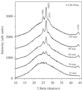
Figure 1 shows the XRD patterns for the A CdS films. The patterns show the increasing presence with deposition time of polycrystalline structure in these films, displaying diffraction lines at about 25, 26.5, 28.2 and 44°, situated on a broad reflection produced by the amorphous substrate. The four peaks are produced by the (100), (002), (101) and (110) crystalline planes, respectively, of the hexagonal CdS structure. The increase in intensity of the crystalline peaks with deposition time is due to the increase of the film thickness. The relative intensity of the (002) reflection indicates a preferred orientation along the [002] direction. These results are in agreement with structural data reported in the literature for chemically deposited CdS films prepared with a similar reaction solution35. Figure 2 shows the XRD
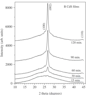
patterns for the B CdS films. These patterns also display the (100), (002) and (110) diffraction lines of the hexagonal CdS structure. However, the (101) diffraction line does not appear or is very weak. The intensity of the peaks (i.e., film thickness) also increases with deposition time. The ratio of the (002) peak intensity to the (100) and (110) peak intensity is much larger than for the A films, indicating a stronger [002] preferred orientation. It is known that the surface mobility of adsorbed species at the substrate surface has a strong influence on the crystalline structure during the growth process37. For example, an amorphous layer,
Figure 1. X-ray diffraction patterns of the A CdS films deposited for 15, 30, 60, 90 and 120 minutes.
highly disordered, is obtained when the mobility of the species arriving to the substrate is very low. On the other hand, crystalline layers with high crystalline orientation can be obtained when the mobility of the species is high. The initial pH in solution A is 11.6, which means a higher concentration of OH– ions and thus faster generation of S2–
ions by the thermal hydrolysis of thiourea. The nucleation of a precipitate in the reaction solution begins in some local regions with inhomogeneities where the ionic product is larger than the solubility product22. The subsequent growth
of these precipitates by the addition of more ions from the solution results in the formation of stable clusters in the solution which can be deposited on the film. The lower mobility of the cluster adsorbed to the substrate surface could be the origin of the lower preferred orientation observed in the A films relative to the B films. In fact, we have shown in a previous paper that the A films indeed do grow by the cluster by cluster mechanism31. On the other
hand, the lower initial pH in solution B and the control of the pH during deposition avoids or diminishes the creation of inhomogeneous regions in the solution, promoting the direct reaction of elementary species at the substrate surface (e.g., promoting ion by ion deposition of the films). The lighter ions adsorbed to the substrate have higher mobility and thus provide the origin of the higher preferred orientation observed in the B films.
Figures 3 and 4 show the absorption spectra obtained from the A and B films, respectively. In both figures the spectra show an absorption edge at about 490 nm due to the fundamental absorption of CdS. The optical density at lower wavelengths (< 490 nm) increases with the deposition time of the films because of the increase in film thickness. From these spectra the energy band gap, Eg, of the films was obtained. To accomplish this, (OD*E)2 was plotted versus
E and the model for direct allowed transitions between
parabolic energy bands was applied38. Here, OD is the
optical density, and E is the photon energy. The insets in Figures 3 and 4 show the (OD*E)2 versus E graphs, with the
linear fit (solid line) to the experimental data (dotted line), for the films deposited for 60 minutes. By averaging the values of Eg obtained for each type of film, we found that both types of CdS film have a similar average of ~2.58 eV. This value of Eg is larger than the value reported for bulk CdS and for that of other chemically deposited CdS films prepared using different reaction solutions7,9,10.
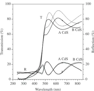
The growth kinetics for the deposition processes was determined from transmission and reflection spectroscopy. The transmission and reflection spectra for the A and B films deposited for 120 minutes are shown in Figure 5. They have the same absorption edge at ~500 nm. The transmission of the films at larger wavelengths than the absorption
Figure 2. X-ray diffraction patterns of the B CdS films deposited for 15, 30, 60, 90 and 120 minutes.
Figure 3. Optical absorption spectra of the A CdS films. The inset is the (OD*E)2 versus E graph, with the linear fit (solid line) to the experimental data (dotted line), for the film deposited for 60 minutes.
Ortuño-López et al.
edge is between 70 and 90% and drops to 10 % at lower wavelengths. The reflectance of the films is between 10 and 20% over the entire wavelength range. In these spectra the absorption edge of CdS is also manifested at about 500 nm. The oscillations of both transmission and reflection of the films in the semi-transparent region are due to interference with the light reflected at the substrate-layer interface. The transmission and reflection spectra of the CdS films were fitted by the Tauc-Lorentz model using a two-layer system representing the glass substrate and the CdS layer39,40. In
this model, the dispersion relation is given by the product of the Tauc joint density of states above the band edge for amorphous materials and the imaginary part of the Lorentz harmonic oscillator dielectric function. Therefore, the expression for the imaginary part of the dielectric function as a function of photon energy, ε2(E), for E >Eg, is given by
2 2
2 0
2 2 2 2 2 2
1 0
( ) ( ) 1
( )
[ ( ) ]
j j g
j j
A E E E
E
E
E E E
=
ν −
ε = ⋅
− + ν
∑ (1)
where j is the number of oscillators (two were considered in our case), A is the amplitude, E0 the central energy and
ν the damping coefficient for each oscillator. For E < Eg,
ε2(E)=0. The real part of the dielectric function, ε1(E), is
obtained by means of Kramer-Kronig integration
2
1 2 2
( ) 2
( )
g E
E P d
E
∞
∞ ξε ξ
ε = ε + ξ
π ∫ ξ − (2)
where ε∞ is the high frequency lattice dielectric constant, ξ
is an integration energy variable and P denotes the principal value of the integral. The optical measurement system used for the T and R measurements includes the software (Film Wizard®) to perform the fits of this model to experimental
optical spectra. The best fits for each spectrum are plotted as discontinuous lines in Figure 5. As observed in the figure, the
reflectance spectra fit quite well to the model over the entire wavelength range. The transmission spectra fit very well below the absorption edge, but in the semi-transparent region there is a distinct discrepancy; the experimental transmission is lower than the simulated data. This discrepancy could be due to the loss of light due to scattering by the films.
From the fits of the spectra we obtained the complex dielectric function, ε1+iε2,and thickness of both types of
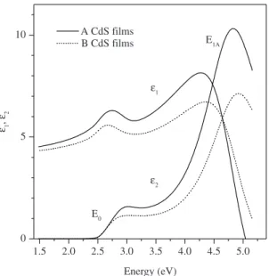
films. The real, ε1,and complex, ε2, components of the complex dielectric function of the CdS films as a function of photon energy are shown in Figure 6. The spectra plotted with continuous lines correspond to the A films, and the spectra in dotted lines correspond to the B films. The shapes of the ε1 and ε2 spectra, respectively, are very similar for
the two types of film, the spectra of A films having higher intensity, which in the case of the ε1 spectrum is related to the refraction index and is evidence of more compact films40.
Two transitions can be observed in these spectra indicated by E0 and E1A in the ε2 spectra. The first transition at about
2.5 eV is due to the absorption of light at the fundamental gap, E0, of CdS. The energy, E1A , at about 4.8 eV represents the energy of the transitions along the Γ→A direction of the Brillouin zone of the CdS wurtzite lattice41. The shape of
the spectra and the energy of the transitions at the critical points measured in the CdS films agree with those measured in hexagonal CdS crystals by means of spectroscopic ellipsometry41.
Figure 7 shows the thickness of the films as a function of deposition time, obtained from the fittings of the transmission/reflection versus wavelength curves for all samples (as shown for the 120 minutes. samples in Figure 5). Initially a fast and almost linear increase in thickness is observed for both the A and B reactions. The thickness is about 40 nm for both types of film after 15 minutes of deposition, and it increases up to 240 and 290 nm for A and B films, respectively, after 120 minutes. of deposition. From these results it can be concluded that the deposition process for the B films produces a higher deposition rate, higher final film thickness and also higher effective termination time (i.e., the time necessary to attain the final film thickness). The differences could be related to the difference in the initial value of the pH of the solutions and to the better pH control of the B solution during growth. The pH control is achieved by the addition of NH4OH/NH4Cl as a buffer, which controls the amount of free OH– ions in the reaction solution. Buffers
are usually mixtures of weak acids or bases and their salts. The buffering action of this solution can be understood by considering the following equilibrium equations:
3 2 4
NH + H ONH ++ OH− (3)
3 4
NH + H+NH + (4)
If extra OH– ions are added to the solution, the equilibrium
is shifted to the left in Equation 3; it tends to remove OH–
ions. On the other hand, if H+ ions are added, they are
consumed to convert ammonia to NH4+ ions (Equation 4).
The OH– ions are necessary for the nucleation (Equation 5)
and CdS synthesis (Equation 6) stages of the CBD process,
Figure 5. Experimental (solid lines) and theoretical (dotted lines) transmission and reflection spectra of the A and B CdS films deposited for 120 minutes.
a faster formation of stable clusters with the consequent homogeneous CdS precipitation in the solution. Thus, there will be less available elementary species to be incorporated in the film, yielding a decrease in the deposition rate and the final film thickness.
4. Conclusions
By comparing the properties of the CdS films we can conclude that the lower initial pH and the control of the pH by adding a pH-10 buffer to the reaction solution to grow the B CdS films produces hexagonal CdS films with a higher degree of preferred orientation along the [002] crystalline direction. The use of the buffer also increases the growth kinetics, resulting in thicker films. However, the optical properties, such as energy band gaps at the critical points of the electronic band structure of CdS, are not affected by the use of the buffer.
Acknowledgements
We acknowledge the technical assistance of M. A. Hernández Landaverde and J.E. Urbina Alvárez. We also thank Dr. Michael S. Boldrick for his helpful review of and comments on the manuscript. This work was partially supported by CONACyT (Project No. CB-2008-01-106952).
Figure 6. Dielectric function spectra ε1(E) and ε2(E)of the A (solid lines) and B (dotted lines) CdS films deposited for 120 minutes.
Figure 7. Thickness of the A and B CdS films as a function of deposition time.
reacting with Cd+2 ions to form Cd(OH)
2 nuclei and then
CdS by reaction with S–2 ions from the thermal hydrolysis
process of thiourea (Equations 7a and 7b), according to the following chemical reactions:
( )
2
2(s)
Cd+ + 2OH−Cd OH (5)
2 2
(s)
Cd+ + S− CdS (6)
(
)
222 2 2 2
SC NH + 2OH−S− + H O + CN H (7a)
2 2
HS−+ OH −→S− + H O (7b)
It has been found that deposition rate of CdS films that grow by the ion by ion process increases with the pH of the initial reaction solution22. This explanation does not apply to
this study. Rather, the higher deposition rate of the B films is a consequence of the lower initial pH and the pH control of the reaction solution. As stated above, the higher initial pH and the lack of control of the pH in the A solution produces
References
1. Nair PK and Nair MTS. Solar-assisted chemical deposition of highly photosensitive CdS thin films. Solar Energy Materials. 1987; 15:431-440. http://dx.doi.org/10.1016/0165-1633(87)90092-X
2. Lincot D and Ortega-Borges R. Chemical bath deposition of cadmium sulfide thin films. In situ growth and structural studies by combined quartz crystal microbalance and electrochemical impedance techniques. Journal of the Electrochemical Society. 1992; 139:1880-1889. http://dx.doi. org/10.1149/1.2069515
3. Doña JM and Herrero J. Chemical bath deposition of CdS thin films: An approach to the chemical mechanism through study of the film microstructure. Journal of the Electrochemical Society. 1997; 144:4081-4091. http://dx.doi. org/10.1149/1.1838140
Ortuño-López et al.
5. Bhattacharyya D and Carter. Effect of substrate on the structural and optical properties of chemical-bath-deposited CdS films. Thin Solid Films. 1996; 288:176-181. http://dx.doi. org/10.1016/S0040-6090(96)08806-2
6. Niles DW, Herdt G and Al-Jassim M. An x-ray photoelectron spectroscopy investigation of O impurity chemistry in CdS thin films grown by chemical bath deposition. Journal of Applied Physics. 1997; 81:1978-1984. http://dx.doi. org/10.1063/1.364054
7. Zelaya-Angel O, Esparza-García AE, Falcony C, Lozada-Morales R and Ramírez-Bon R. Photoluminescence effects associated with thermally induced crystalline structure changes in CdS films. Solid State Communications. 1995; 94:81-85. http://dx.doi.org/10.1016/0038-1098(94)00840-X
8. Shao M, Fischer A, Grecu D, Jayamaha U, Bykov E, Contreras-Puente G et al. Radio-frequency-magnetron-sputtered CdS/CdTe solar cells on soda-lime glass. Applied Physics Letters. 1996; 69:3045-3047. http://dx.doi. org/10.1063/1.116834
9. Ramírez-Bon R, Sandoval-Inda NC, Espinoza-Beltrán FJ, Sotelo-Lerma M, Zelaya-Angel O and Falcony C. Structural transition of chemically deposited CdS films on thermal annealing. Journal of Physics: Condensed Matter. 1997; 9:10051-10058. http://dx.doi.org/10.1088/0953-8984/9/45/031
10. Oliva AI, Solís-Canto O, Castro-Rodríguez R and Quintana P. Formation of the band gap energy on CdS thin films growth by two different techniques. Thin Solid Films. 2001; 391:28-35. http://dx.doi.org/10.1016/S0040-6090(01)00830-6
11. Zehe A and Vázquez-Luna JG. Magnetic field influenced growth kinetics in chemical CdS thin-film deposition. Solar Energy Materials and Solar Cells. 2001; 68:217-226. http:// dx.doi.org/10.1016/S0927-0248(00)00234-8
12. Mendoza-Pérez R, Santana-Rodríguez G, Sastre-Hernández J, Morales-Acevedo A, Arias-Carbajal A, Vigil-Galán O et al. Effects of thiourea concentration on CdS thin films grown by Chemical Bath Deposition for CdTe solar cells. Thin Solid Films. 2005; 480-481:173-176. http://dx.doi.org/10.1016/j. tsf.2004.11.060
13. Matsune K, Oda H, Toyama T, Okamoto H, Kudriavysev Y and Asomoza R. 15% Efficiency CdS/CdTe thin film solar cells using CdS layers doped with metal organic compounds. Solar Energy Materials and Solar Cells. 2006; 90:3108-3114. http://dx.doi.org/10.1016/j.solmat.2006.06.030
14. Mendoza-Pérez R, Aguilar-Hernández J, Sastre-Hernández J, Ximello-Quiebras N, Contreras-Puente G, Santana-Rodríguez G et al. Photoluminescense characteristics of the CdS layers deposited in a chemical bayh and their correlation to CdS/CdTe. Solar Energy. 2006; 80:682-686. http://dx.doi.org/10.1016/j. solener.2006.01.002
15. Morales-Acevedo A. Thin film CdS/CdTe solar cell: Research perspective. Solar Energy. 2006; 80:675-681. http://dx.doi. org/10.1016/j.solener.2005.10.008
16. Altosaar M, Danilson M, Kauk M, Krustok J, Mellikov E, Raudota J et al. Further developments in CIS monograin layer solar cells technology. Solar Energy Materialsand Solar Cells. 2005; 87:25-32. http://dx.doi.org/10.1016/j. solmat.2004.09.021
17. Canava B, Guillemoes JF, Yousfi EB, Cowache P, Kerber H, Loeff A et al. Wet treatment based interface engineering for high efficiency Cu(In,Ga)Se2 solar cells. Thin Solid Films. 2000; 361:187-192. http://dx.doi.org/10.1016/S0040-6090(99)00861-5
18. Contreras MA, Romero MJ and Noufi R. Characterization of Cu(In,Ga)Se2 materials used in record performance solar cells. Thin Solid Films. 2006; 511-512:51-54. http://dx.doi. org/10.1016/j.tsf.2005.11.097
19. Bayhan H and Sertap Kavasoglu A. Study of CdS/Cu(In, Ga) Se2 heterojunction interface using admittance and impedance spectroscopy. Solar Energy. 2006; 80(9):1160. http://dx.doi. org/10.1016/j.solener.2005.09.004
20. Li W, Sun Y, Liu W and Zhou L. Fabrication of Cu(In,Ga)Se2 thin films solar cell by selenization process with Se vapor. Solar Energy. 2006; 80:191-195. http://dx.doi.org/10.1016/j. solener.2005.07.011
21. Chopra KL and Ranjan Das S. Thin Film Solar Cells. New York and London: Plenum Press; 1983.
22. Kaur I, Pandya DK and Chopra KL. Growth Kinetics and Polymorphism of Chemically Deposited CdS Films. Journal of the Electrochemical Society. 1980; 127:943-948. http://dx.doi. org/10.1149/1.2129792
23. Ferekides CS, Balasubramanian U, Mamazza R, Viswanathan V, Zhao H and Morel DL. CdTe thin film solar cells: device and technology issues. Solar Energy. 2004; 77:823-830. http:// dx.doi.org/10.1016/j.solener.2004.05.023
24. Contreras MA, Romero MJ, To B, Hasoon F, Noufi R, Ward S et al. Optimization of CBD CdS process in high-efficiency Cu(In,Ga)Se2-based solar cells. Thin Solid Films. 2002; 403-404:204-211. http://dx.doi.org/10.1016/ S0040-6090(01)01538-3
25. Ochoa-Landín R, Sastre-Hernández J, Vigil-Galan O and Ramírez-Bon R. Chemically deposited CdS by an ammonia-free process for solar cells window layers. Solar Energy. 2010; 84:208-214. http://dx.doi.org/10.1016/j. solener.2009.11.001
26. Arreola-Jardón G, González LA, García-Cerda LA, Gnade B, Quevedo-López MA and Ramírez-Bon R. Ammonia-free chemically deposited CdS films as active layers in thin film transistors. Thin Solid Films. 2010; 519:517-520. http://dx.doi. org/10.1016/j.tsf.2010.08.097
27. Salas-Villaseñor AL, Mejía I, Hovarth J, Alshareef HN, Cha DK, Ramírez-Bon R et al. Impact of gate dielectric in carrier mobility in low temperature chalcogenide thin film transistors for flexible electronics. Electrochemical and Solid State Letters. 2010; 13:H313-H316. http://dx.doi. org/10.1149/1.3456551
28. Chang Y-J, Munsee CL, Herman GS, Wager JF, Mugdur P, Lee D-H et al. Growth, characterization and application of CdS thin films deposited by chemical bath deposition. Surface and Interface Analysis. 2005; 37:398-405. http://dx.doi. org/10.1002/sia.2012
29. Gan FY and Shih I. Preparation of thin-film transistors with chemical bath deposited CdSe and CdS thin films. IEEE Transactions on Electronic Devices. 2002; 49:15-18. http:// dx.doi.org/10.1109/16.974742
30. Voss C, Subramanian S and Chang C-H. Cadmium sulfide thin-film transistors fabricated by low-temperature chemical-bath deposition. Journal of Applied Physics. 2004; 96:5819-5822. http://dx.doi.org/10.1063/1.1804244
31. Sandoval-Paz MG, Sotelo-Lerma M, Mendoza-Galván A and Ramírez-Bon R. Optical properties and layer microstructure of CdS films obtained from an ammonia-free chemical bath deposition process. Thin Solid Films. 2007; 515:3356-3362. http://dx.doi.org/10.1016/j.tsf.2006.09.024
32. Sandoval-Paz MG and Ramírez-Bon R. Analysis of the early growth mechanisms during the chemical deposition of CdS thin films by spectroscopic ellipsometry. Thin Solid
Films. 2009; 517:6747-6752. http://dx.doi.org/10.1016/j. tsf.2009.05.045
33. Kariper A, Güneri E, Göde F, Gümüş C and Özpozan T. The structural, electrical and optical properties of CdS thin films as a function of pH. Materials Chemistry and Physics. 2011; 129:183-188. http://dx.doi.org/10.1016/j. matchemphys.2011.03.070
34. Zhou L, Hu X and Wu S. Effects of pH value on performance of CdS films with chemical bath deposition. Advanced Materials Research. 2012; 557-559:1941-1944. http://dx.doi. org/10.4028/www.scientific.net/AMR.557-559.1941 35. George PJ, Sánchez A, Nair PK and Nair MTS. Doping of
chemically deposited intrinsic CdS thin films to n type by thermal diffusion of indium. Applied Physics Letters. 1995; 66:3624-3626. http://dx.doi.org/10.1063/1.113808
36. Castillo SJ, Sotelo-Lerma M, Neyra I, Ortuño M, Ramírez-Bon R and Espinoza-Beltrán FJ. Effects of reaction temperature on the physical properties of chemically deposited CdS films. Materials Science Forum. 1998; 287-288:343-346.
37. Chopra KL. Thin Film Phenomena. New York: McGraw-Hill; 1969.
38. Pankove JI. Optical Processes in Semiconductors. New York: Dover Publications Inc.; 1971.
39. Ortuño-López MB, Sotelo-Lerma M, Mendoza-Galván A and Ramírez-Bon R. Chemically deposited CdS films in an ammonia-free cadmium–sodium citrate system. Thin Solid Films. 2004; 457:278-284. http://dx.doi.org/10.1016/j. tsf.2003.11.169
40. Ochoa-Landín R, Sandoval-Paz MG, Ortuño-López MB, Sotelo-Lerma M and Ramírez-Bon R. Observations on the influence of pH control on the properties of chemically deposited CdS films in an ammonia-free system. Journal of Physics and Chemistry of Solids. 2009; 70:1034-1041. http:// dx.doi.org/10.1016/j.jpcs.2009.05.020