Brazilian Journal of Physics, vol. 34, no. 2B, June, 2004 547
STM Light Emission Spectroscopy of Individual Quantum Wells:
Measurement of Transport Parameters in Real Space
S. Ushioda
∗, T. Tsuruoka
∗, Y. Ohizumi
†, and H. Hashimoto
† ∗Photodynamics Research Center, RIKEN, Sendai 980-0845, Japan
†
Research Institute of Electrical Communication, Tohoku University, Sendai 980-8577, Japan
Received on 31 March, 2003
By spectroscopically analyzing the light emitted from the tip-sample gap of the scanning tunneling microscope (STM), we have investigated the carrier transport as well as the luminescence properties of AlGaAs/GaAs quantum wells (QW’s). The emission intensity form a target well was measured as a function of the tip position on a cleaved (110) surface of the QW structures. The thermalization length and the diffusion length of the injected electrons were determined in real space.
1
Introduction
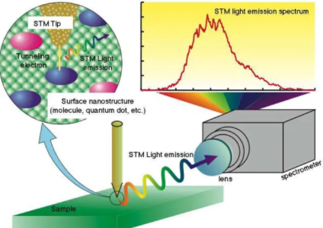
Visible light is emitted when electrons or holes are injected from the tip of the scanning tunneling microscope (STM). By spectroscopic analysis of this emission, one can charac-terize nanometer scale objects (nanostructures) with atomic-scale spatial resolution. We are utilizing this effect to study the electronic transitions in individual surface nanostruc-tures such as quantum wells (QW’s), quantum dots (QD’s), and atoms and molecules adsorbed on solid surfaces. In this method one first observes the STM image of the surface to-pography and finds the nanostructures of interest. Then the STM tip is located over the target structure and the tunnel-ing current is injected into the specific individual target. The spectrum of the emitted light is measured with the STM tip fixed over the target, thus obtaining information on the elec-tronic transitions of the individual target nanostructure. This method is shown schematically in Fig. 1.
Figure 1. Experimental concept of STM light emission.
We have applied this spectroscopic technique with an atomic scale spatial resolution to several sample systems,
including QW’s [1,2], QD’s [3], and surface adsorbed atoms and molecules [4,5]. In this talk we will focus on the measurement of the electron thermalization and diffusion lengths in real space in AlGaAs/GaAs QW structures [6,7]. The details of the sample and STM setup are shown in Fig. 2.
[001] [110] UHV-STM chamber
Optical fiber
Mono-chromator CCD camera
Sample
Optical fiber
Sample holder
Tip
STM tip
(110) surface Base pressure = 5 ~ 10-9 Pa
STM
Solid angle of collection = 0.13 sr
Figure 2. Setup for STM light emission spectroscopy.
2
Experiment and Results
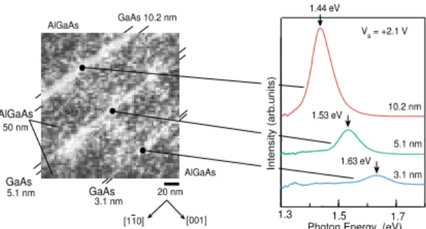
The sample was grown by molecular-beam epitaxy (MBE) on a p-type GaAs(001) substrate. It had p-GaAs QW’s of widths 3.1, 5.1, and 10.2 nm sandwiched between the bar-rier layers of p-Al0.3Ga0.7As whose width was 50 nm. The
hole concentration was 2×1019 cm−3 for the GaAs QW,
and 1.4×1019 cm−3 for the AlGaAs barrier layers. This
548 S. Ushiodaet al.
20 nm GaAs
GaAs GaAs 10.2 nm
5.1 nm 3.1 nm AlGaAs AlGaAs AlGaAs [001] [110] 50 nm 10.2 nm 5.1 nm 1.44 eV 1.53 eV 1.63 eV 3.1 nm
Photon Energy (eV)
1.3 1.5 1.7
Intensity (arb
.units)
Vs = +2.1 V
Figure 3. STM image of cleaved AlGaAs/GaAs QW structures and light emission spectra measured over the three wells.
The emission spectra from the three wells are shown in Fig. 3. We see that the peak energy shifts to higher energies as the well width decreases. This is a direct demonstration of the quantum confinement effect. Since the peak ener-gies of the emission from the different wells can be clearly identified , one can know the relative number of electrons that reach each well from the intensity of the corresponding peak. We measured the intensity from different wells as a function of the distance between the injection point and the position of the wells. The emission intensity vs. distance is plotted for the 10.2 nm QW in Fig. 4. The intensity de-cay curve can be fitted by assuming two exponential dede-cay lengths L1and L2as shown in Fig. 4.
Figure 4. Logarithmic plot of emission intensity from 10.2 nm well as a function of tip position. The dotted and dashed lines are the
exponential decay functions with different decay constants L1and
L2. The solid curve is the superposition of the dotted and dashed
lines.
We identified these two decay distances as the thermal-ization length and the diffusion length by comparing the ex-perimental decay curve with the results of Monte Carlo sim-ulation. The thermalization length is the mean distance that the injected electron travels before thermally relaxing to the bottom of the conduction band through scattering processes with phonons, optical phonon-plasmon coupled modes, ion-ized impurities, etc. The diffusion length is the mean dis-tance that the electron propagates before getting lost by re-combination processes. Fig. 5 shows the electron number
decay curves for the three wells when the bias voltage VSis +2.5 V. Fig. 6 shows the corresponding data for VS = +2.1 V.
By comparing the data in Figs. 5 and 6, we see that the thermalization length depends on the electron injection en-ergy that is determined by the bias voltage of the tunneling, i. e. on the energy level at which electrons tunnel into the conduction band. When the injection energy gets higher (VS = +2.5 V), the thermalization length gets longer than for the case of lower injection energy (VS = +2.1 V). On the other hand the diffusion length is independent of the bias voltage. This result is reasonable, when one realizes that higher en-ergy electrons will take a larger number of scattering events before they thermalize down to the bottom of the conduction band. ✁ ✁ ✁ ✁ ✁ ✁ ✁ ✁ ✁ ✁ ✁ ✁ ✁ ✁ ✁ ✁ ✁ ✁ ✁ ✁✁ ✁ ✁ ✁ ✁ ✁ ✁ ✁ ✁ ✁ ✁ ✁ ✁ ✁ ✁ ✁ ✁ ✁ ✁ ✁ ✁ ✂ ✂ ✂ ✂ ✂ ✂ ✂ ✂ ✂ ✂ ✂ ✂ ✂ ✂ ✂ ✂ ✂ ✂ ✂ ✂ ✂ 0.1 1 10 100
-120 -100 -80 -60 -40 -20 0 20 40 60 80 100 120
Tip Position (nm)
30 17 17 14 14 16 200 200 200 200 200 200 Ln(Intensity) (cps)
VS = +2.5 V
3.1nm well 5.1nm well 10.2nm well
Figure 5. Logarithmic plot of emission intensity from the three
wells as a function of tip position for VS = +2.5 V. The solid
squares, circles, and triangles represent the data for the wells of 10.2, 5.1, and 3.1 nm widths. The dotted and dashed lines are
the exponential decay functions with different decay constants L1
and L2. The solid curves are the superpositions of the dotted and
dashed lines.
Fig. 5. Logarithmic plot of emission intensity from the three wells as a function of tip position for VS = +2.5 V. The solid squares, circles, and triangles represent the data for the wells of 10.2, 5.1, and 3.1 nm widths. The dotted and dashed lines are the exponential decay functions with different decay constants L1 and L2. The solid curves are the superpositions of the dotted and dashed lines.
✁ ✁ ✁ ✁ ✁ ✁ ✁ ✁ ✁ ✁ ✁ ✁ ✁ ✁ ✁ ✁ ✁ ✁ ✁ ✁ ✁ ✁ ✁ ✁✁ ✁ ✁ ✁ ✁ ✁ ✁ ✂ ✂ ✂ ✂ ✂ ✂ ✂ ✂ ✂ ✂ ✂ ✂ ✂ ✂ ✂ ✂ ✂ ✂ ✂ ✂ ✂ 0.1 1 10 100
-120 -100 -80 -60 -40 -20 0 20 40 60 80 100 120 Tip Position (nm)
7 6 5 150 150 200 150 5 6 7 150 150 Ln(Intensity) (cps)
VS = +2.1 V
3.1nm well 5.1nm well 10.2 nm well
Fig. 6. Logarithmic plot of emission intensity from the three wells as a function of tip position for VS = +2.1 V. The data are fitted by the theoretical decay curves with two distinct decay constants in the same manner as in Fig. 5.
III. Conclusion
In conclusion, we have demonstrated that the thermalization and diffusion lengths of injected electrons in QW structures can be measured in real space by using the atomic-scale spatial resolution of the STM light emission spectroscopy. This technique is very powerful in evaluating nanostructures relevant to nanotechnology.
Acknowledgement
We gratefully acknowledge valuable advice from Prof. J. Nishizawa. We are also indebted to members of our research group, Y. Uehara, K. Sakamoto, and R. Arafune for their cooperation.
References
[1] T. Tsuruoka, Y. Ohziumi, S. Ushioda, Y. Ohno, and H. Ohno, Appl. Phys. Lett. 73, 1544 (1998). [2] T. Tsuruoka, Y. Ohizumi, R. Tanimoto, and S.
Ushioda, Appl. Phys. Lett. 75, 2289 (1999). [3] T. Tsuruoka, Y. Ohizumi, and S. Ushioda, Appl.
Phys. Lett. 82, 3257 (2003); J. Appl. Phys. 95, 1064 (2004).
[4] Y. Uehara, T. Matsumoto, and S. Ushioda, Solid State Commun. 122, 451 (2002); Phys. Rev. B 66, 075413 (2002).
[5] K. Sakamoto, K. Meguro, R. Arafune, M. Sato, Y. Uehara, and S. Ushioda, Surf. Sci. 502-503, 149 (2002).
[6] T. Tsuruoka, R. Tanimoto, Y. Ohizumi, R. Arafune, and S. Ushioda, Appl. Phys. Lett. 80, 3748 (2002); Appl. Surf. Sci. 190, 275 (2002). [7] T. Tsuruoka, H. Hashimoto, Y. Ohizumi, and S.
Ushioda, Inst. Phys. Conf. Ser. 174. 61 (2003).
3
Figure 6. Logarithmic plot of emission intensity from the three
wells as a function of tip position for VS= +2.1 V. The data are
fitted by the theoretical decay curves with two distinct decay con-stants in the same manner as in Fig. 5.
3
Conclusion
Brazilian Journal of Physics, vol. 34, no. 2B, June, 2004 549
can be measured in real space by using the atomic-scale spa-tial resolution of the STM light emission spectroscopy. This technique is very powerful in evaluating nanostructures rel-evant to nanotechnology.
Acknowledgement
We gratefully acknowledge valuable advice from Prof. J. Nishizawa. We are also indebted to members of our re-search group, Y. Uehara, K. Sakamoto, and R. Arafune for their cooperation.
References
[1] T. Tsuruoka, Y. Ohziumi, S. Ushioda, Y. Ohno, and H. Ohno,
Appl. Phys. Lett.73, 1544 (1998).
[2] T. Tsuruoka, Y. Ohizumi, R. Tanimoto, and S. Ushioda, Appl. Phys. Lett.75, 2289 (1999).
[3] T. Tsuruoka, Y. Ohizumi, and S. Ushioda, Appl. Phys. Lett.
82, 3257 (2003); J. Appl. Phys.95, 1064 (2004).
[4] Y. Uehara, T. Matsumoto, and S. Ushioda, Solid State
Com-mun.122, 451 (2002); Phys. Rev. B66, 075413 (2002).
[5] K. Sakamoto, K. Meguro, R. Arafune, M. Sato, Y. Uehara,
and S. Ushioda, Surf. Sci.502-503, 149 (2002).
[6] T. Tsuruoka, R. Tanimoto, Y. Ohizumi, R. Arafune, and S.
Ushioda, Appl. Phys. Lett.80, 3748 (2002); Appl. Surf. Sci.
190, 275 (2002).