550 Brazilian Journal of Physics, vol. 34, no. 2B, June, 2004
Semiconductor Quantum Dot Nanostructures and
their Roles in the Future of Photonics
S. Fafard
∗, K. Hinzer
∗†, and C. N. Allen
Institute for Microstructural Research, National Research Council, Canada K1A 0R6
Received on 31 March, 2003
This paper discusses the growth and the properties of semiconductor nanostructures based on self-assembled quantum dots (QDs). These QDs confine electrons or excitons in zero-dimension (0D), similar to an artificial atom or to an artificial molecule in the case of coupled QDs with vertical alignment. They are obtained in a simple step during the epitaxy of strained III-V semiconductors such as InAs on GaAs, or InAs on InP. We will elaborate on the unique optical properties and the physics of self-assembled QDs and their applications, including QD lasers.
1
Introduction
Despite the tough times recently in the telecommunication industry, there is a general feeling that it is approaching a bottom and that innovative devices will enable the next generation of products based on advanced semiconductor and photonic components. Enhanced performance, reduced cost and compact dimensions are a prerequisite for those novel products, and nanostructures could allow the develop-ment of such devices. For example, lasers at 1.3 microns on GaAs, widely tunable lasers and/or multi-wavelength sources, semiconductor optical amplifiers, or more defect-robust devices, or devices which can work at higher tem-peratures, etc. Recently, it has been demonstrated that self-assembled growth can be controlled to systematically and reproducibly fabricate QD structures which have well-defined excited-state transitions, like an artificial atom, and to manipulate their energy levels to tailor the number of confined states and their intersublevel energy-spacing [1]. Moreover, the structural quality of the self-assembled QDs and their compatibility with conventional III-V technology has permitted the demonstration of high performance pro-totype devices such as semiconductor QD lasers [2]. These developments are very promising for QD devices which can yield novel nanostructures with unique properties due to their atomic-like shell configurations [3]. Other examples, include QD infrared detectors which are sensitive in nor-mal incidence detection due to the geometry of the QDs. Also, optical memories based on coupling of QDs can have large storage density. This paper therefore elaborates on some of the unique optical properties and the physics of self-assembled QDs and their applications.
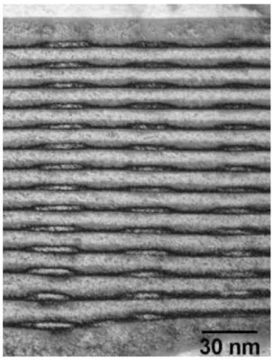
Mutlilayer stacks of QDs can be grown with good uni-formity. For example, Fig. 1 shows the active region of a QD laser with 14 layers where the InAs/GaAs QDs are
uni-form from one layer to the next [4]. This is interesting for improving the gain saturation of QD lasers, but it is also of great interest for coupled QDs. It is possible to engineer the energy levels of such InAs/GaAs QD lasers for emission between∼900nm to∼1350nm.
Figure 1. Laser diode with shape-engineered self-aligned QDs. Cross-section TEM of the active region of the laser diode contain-ing a stack of 14 layers of InAs QDs indium-flushed at 5.0nm and separated by 10.0 nm GaAs spacers, McCaffrey et al. [4].
Figure 2. Emission at T = 77 K from the stack of eleven layers with a 500µm long cavity. (a) State filling spectroscopy with
cur-rent densities varying from 0.003 A/cm2 (bottom) to 213 A/cm2 (lasing threshold) (top). (b) Lasing in an excited states for currents between 230 A/cm2(bottom) and 4.0 kA/cm2(top).
Figure 3. Lasing at T = 77 K from an InAs/GaAs QD laser with a stack of seven layers; (a) 1300µm long cavity for current densities
between 20 A/cm2(bottom) and 120 A/cm2(top), and (b) 500µm
long cavity for current densities between 65 A/cm2 (bottom) and 2.1 kA/cm2(top).
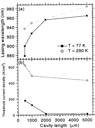
Figure 4. (a) Lasing wavelength, and (b) threshold current density for different laser cavity at T = 77 K and T = 290 K for the sample of Fig. 1.
552 Brazilian Journal of Physics, vol. 34, no. 2B, June, 2004
Figure 5. Temperature dependence of the threshold current den-sities for the three InAs QD samples with long resonant cavities: a stack of seven layers (dash), a the stack of eleven layers (dot), and a larger dot density stack of seven layers (solid). In the inset, threshold current density as a function of the cavity length at T = 77 K for the first 2 samples.
Figure 6. Interband zero-dimensional transitions measured with open circuit photovoltage across QD laser diodes: curve i) is at 77K for a stack of 14 layers indium-flushed at 5.0nm (the laser shown in the TEM in fig. 1), curve ii) is the same laser at 300K, and curve iii) is for a laser diode with a single layer indium-flushed at 8.5nm with a QD ground state close to 1.3µm at 300K.
As mentioned above, QD lasers can also be grown for ∼1.3 micron using the InAs/GaAs material system. Indeed, the 1.3 micron QD lasers have received a lot of attention be-cause of the optoelectronics applications for telecom. In fact 1.3 micron QD lasers are just a different flavor of the near infrared InAs/GaAs QDs using slight variations during the growth of the QDs or cladding materials. Room temperature emission at 1300 nm can be obtained using a distant indium-flush [1] (which leads to more indium segregation) and/or equivalently by using some low concentration InGaAs al-loys near the QDs. Alternatively, others have experimented using InGaNAs alloy for the QD formation. Generally, for InAs/GaAs QD lasers, the best performances have been ob-tained for the longer wavelength emitters.
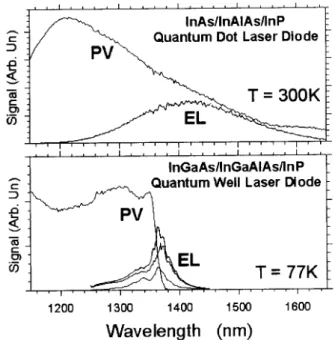
Figure 7. Electroluminescence (EL) and photovoltage (PV) of a QD laser structure (top) and of a control InGaAs/AlInGaAs/InP QW structure grown by MBE.
This is in part because the low energy emission, com-bined with high barriers, leads to large intersublevel energy spacings and good carrier confinement for separate confine-ment heterostructures, and consequently a low thermionic emission and a low temperature quenching of the radiative emission. For the QD lasers emitting around 1.3 micron, record current density thresholds have therefore been ob-served, together with good stability of the characteristic tem-peratures (To). Fig. 5 shows the temperature dependence of the threshold for different QD lasers. The fact that 1.3 micron QD lasers over-performed their quantum well coun-terparts is exciting, but on the other hand the quantum well technology is a very mature and well anchored for the 1.3 micron emitters and unlikely to be replaced in the near fu-ture.
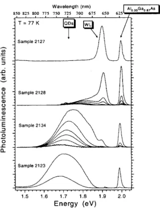
Figure 8. State filling spectroscopy of the AlInAs/AlGaAs samples as a function of excitation intensity. The PL is excited with various intensities up to a few kW/cm2 for the top curve of each sample.
The samples were grown with the equivalent of 0.83nm, 0.86nm, 0.88nm, and 0.90nm of InAlAs from top to bottom respectively.
QDs and an AlGaAs cladding and by studying the intermix-ing [7]. Fig. 9 demonstrates that when the diffusion allows the ternary alloy to be nearby the QDs, the QD excited states are un-resolved. Nevertheless, Fig. 10 demonstrates that the limitations with InAs/GaAs QDs, which have a relatively small confinement energy of the carriers and consequently higher thermionic emission at room temperature, can be cir-cumvented with the use of InAs/GaAs/AlGaAs QDs while preserving a sharp atomic-like shell structure. The emission intensity only decreases by a factor of∼4 between 77K and 300K and well-resolved 0D states are observed at room tem-perature [7].
2
Conclusion
Semiconductor self-assembled QDs demonstrate unique properties related to their similarity to an artificial atoms. They are compatible with standard III-V technology and have no additional defects. These nanostructures have small sizes that yield large confinement energies, and unique prop-erties such as broadband gain/tunability spectra, low chirp, low temperature sensitivity, narrow homogeneous linewidth, and a gain medium robust to material defects.
Figure 9. State-filling spectroscopy at 77K for intermixed InAs/GaAs QDs with nearby AlGaAs barriers (top), and without (bottom). The GaAs spacers are 0.6 nm and 5.6 nm for below and above the WL respectively (top). The PL spectra are obtained with the samples which have received a 30s RTA at the indicated tem-peratures, and exciting with an intensity of∼2 kW/cm2.
Figure 10. A QD ensemble with both, strong carrier confinement and well-resolved excitonic shells. The intensity of the PL, ex-cited with Io∼200 W/cm2, is compared at 77K and at 300K for
InAs/GaAs/AlGaAs QDs with a RTA of 30s at 775o
554 Brazilian Journal of Physics, vol. 34, no. 2B, June, 2004
Acknowledgement
The authors would like to thank many researchers from IMS/NRC who contributed to this work, including Z.R. Wasilewski, J. McCaffrey, M. Spanner, S. Raymond, J. La-pointe, P. Hawrylak.
References
[1] S. Fafard, Z. R. Wasilewski, C. N`ı. Allen, D. Picard, M. Span-ner, J.P. McCaffrey, P.G. Piva, Manipulating the Energy
Lev-els of Semiconductor Quantum Dots, Phys. Rev. B 59, 15368
(1999); B.J. Riel, K. Hinzer, S. Moisa, J. Fraser, P. Finnie, P. Piercy, S. Fafard, Z.R. Wasilewski, InAs/GaAs (100)
Self-Assembled Quantum Dots: Arsenic and Capping Effects, J.
Crystal Growth 236, 145 (2002).
[2] S. Fafard, H.C. Liu, Z.R. Wasilewski, J. McCaffrey, M. Span-ner, S. Raymond, C. N`ı. Allen, K. Hinzer, J. Lapointe, C. Struby, M. Gao, P. Hawrylak, C. Gould, A. Sachrajda, P. Za-wadzki, Quantum dots devices, SPIE 4078, 100 (2000).
[3] M.Bayer, O.Stern, P.Hawrylak, S.Fafard, A. Forchel, Hidden
symmetries in the energy levels of excitonic artificial atoms,
Nature 405, 923 (2000).
[4] J.P. McCaffrey, M.D. Robertson, P.J. Poole, B.J. Riel, S. Fa-fard, ”Interpretation and Modelling of Buried InAs Quantum
Dots on GaAs and InP Substrates”, J. Appl. Phys. 90, 1784
(2001); J.P. McCaffrey, M.D. Robertson, Z.R. Wasilewski, E.M. Griswold, L.D. Madsen, S. Fafard, Determination of
the size, shape, and composition of indium-flushed self-assembled QDs by transmission electron microscopy, J. Appl.
Phys. 88, 2272 (2000)
[5] M. Bayer, P. Hawrylak, K. Hinzer, S. Fafard, M. Korkusin-ski, Z. R. WasilewKorkusin-ski, O. Stern, A. Forchel, Coupling and
Entangling of Quantum States in Quantum Dot Molecules,
SCIENCE 291, 451 (2001).
[6] C. N`ı. Allen, P. J. Poole, P. Marshall, J. Fraser, S. Raymond, and S. Fafard, InAs self-assembled quantum-dot lasers grown
on (100) InP, Appl. Phys. Lett. 80, 3629 (2002).
[7] C. N´ı Allen, P. Finnie, S. Raymond, Z. R. Wasilewski, and S. Fafard, Inhomogeneous broadening in quantum dots with